This document presents an analytical model for the core-shell nanowire junctionless accumulation mode field-effect transistor (csn-jam-fet) tailored for high-frequency applications, showcasing its enhanced performance over traditional nanowire junctionless accumulation mode FET (njam-fet). The csn-jam-fet exhibits improved metrics such as increased drain current, transconductance, output conductance, ion/ioff ratio, and cut-off frequency due to its core-shell architecture. The findings indicate that the csn-jam-fet is a promising candidate for digital applications, offering superior performance characteristics compared to its counterparts.
![ORIGINAL PAPER
Core-Shell Nanowire Junctionless Accumalation Mode Field-Effect
Transistor (CSN-JAM-FET) for High Frequency
Applications - Analytical Study
Sonam Rewari1
Received: 9 September 2020 /Accepted: 28 September 2020
# Springer Nature B.V. 2020
Abstract
Here, an analytical model has been proposed for Core-Shell-Nanowire-Junctionless-Accumulation-Mode- Field-Effect
Transistor (CSN-JAM-FET) for High Frequency Applications. CSN-JAM-FET has been contrasted with Nanowire-
Junctionless- Accumulation- Mode- Field-Effect Transistor (NJAM-FET) under the similar device conditions by keeping the
threshold voltage same for both. It is so found that CSN-JAM-FET shows much higher drain current (Ids), transconductance (gm),
output conductance (gd), Ion/Ioff ratio, Subthreshold Slope (SS) and cut off frequency (fT) because of the inherent property of core
shell architecture to elevate the gate domination over the channel. The analytical results have also been modelled for CSN-JAM-
FET by finding a result of the Two-Dimensional Poisson equation in accordance with the boundary conditions. The analytical
results are much in coherence with the results obtained from the simulator.
Keywords Core-Shell . Junctionless Accumulation Mode . Nanowire . Analog
1 Introduction
An incredible change is observed in the semiconductor commerce
and the evolution still remains never ending and the device length
is being constantly reduced for Ultra Large Scale Integrations
(ULSI) [1]. Even in sub-0.1 μm many SCEs, which deeply the
overall scalability of the device, such as increment in the sub-
threshold slope (SS), which demands consideration [2]. Potential
of silicon technologies beyond 100 nm regime has been well
indicated by modeling and simulation [3–5]. To combat the ef-
fects of SCEs, many variants of device designs have been recom-
mended and deeply studied by the researchers. The Gate All
Around (GAA)/ Nano.
Wire (NW) structures had been the most encouraging de-
vice structure for MOSFETs beyond 10 nm regime [6–11].
Nonetheless, the NW device structures require to be stacked
into arrays to excerpt an agreeable drive current, so that the
chip area is exhausted appreciably opposing the benefits of
scaling. The exploration of FET structures for an improvised
output drive current from the three-dimensional topologies,
has led to the coinage of silicon Nano-Tube (NT) with core
gate structure. Nanotube / Core-Shell architecture is being
investigated these days which combats the SCE’s of GAA/
Nanowire MOSFETs [12–18]. This superior gate control also
administers exquisite amnesty towards the SCEs and a com-
petent volume inversion, leading to high drive currents in
addition to the impressive employment of the real-estate [14,
15, 19].This architecture provides a superlative gate control as
compared to all its counterpart NW device architectures
[12–17]. Technically, lately proposed Junctionless (JL)
MOSFETs have massively doped channel, matching both
the type and the concentration magnitude of the drain and
the source. It thus becomes a uniformly doped resistor [20].
It performance has further been improved by Junctionless
Accumulation Mode (JAM) FET [21, 22]. Truancy of doping
gradient across the channel, source and drain, waives off the
impurities diffusion and hence the dilemma of the sharp dop-
ing profile creation. Thus combining the advocated perks of
Junctionless (JL) and Nanotube (NT) structures, which in-
cludes benign scaling in the short channel regime, comfortable
fabrication (since no sharp doping gradient required), close to
ideal subthreshold slope (SS) and elevated mobility of the
carriers as the conduction path now is at the center (as opposed
* Sonam Rewari
rewarisonam@gmail.com
1
ECE Department, Delhi Technological University,
New Delhi 110042, India
https://doi.org/10.1007/s12633-020-00744-3
/ Published online: 10 October 2020
Silicon (2021) 13:4371–4379](https://image.slidesharecdn.com/7-240902094633-211cbca8/85/NWCore-shell-FET-for-high-frequency-applications-1-320.jpg)
![to the surface potential), which offers less scattering. We here
in this paper, compare the performance of Core-Shell-
Nanowire-Junctionless-Accumulation-Mode- Field-Effect
Transistor (CSN-JAM-FET) with the conventional
Nanowire-Junctionless-Accumulation-Mode- Field-Effect
Transistor (NJAM-FET).
The manuscript is structured in such a way that II section
talks about the device structure, along with the model, and its
calibration. In section III enlists the analytical model proposed
and section IV gives the various performance measures of
CSN-JAM-FET is plotted and presented along with the other
analytical results. Section V concludes the results discussed.
The said device professes and demonstrates preferably admi-
rable performance characteristics.
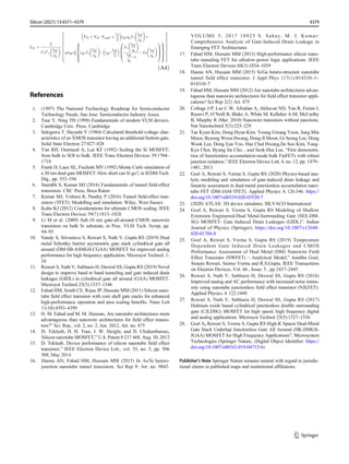
2 Device Design and Simulation
Core-Shell Nanowire Junctionless Accumulation Mode Field-
Effect Transistor (CSN-JAM-FET) Three-Dimensional structure
is pictured in Fig. 1a 2-D correctional glimpse of CSN-JAM-
FET is delineated in Fig. 1b. Structurally, the channel forms
the base, over which the silicon dioxide has been grown, topped
with metal gates with tweakable work-functions [8]. Each metal
has a varied work-function. Table 1 enlists the Device
Specifications. ATLAS-3D device-simulator has been exploited
to carry out numerical simulations [23]. The installation of dif-
ferent work-functions for metal, leads to two gates, i.e., Outer
gate and Inner gate, both with two metal implants each.
Silvaco ATLAS 3-D device-simulator [23] has been de-
ployed to realize the device-simulations. The simulation
models exploited to realize our simulations along with their
descriptions have been tabulated in Table 1.
3 Analytical Model
Mathematical interpretations for Subthreshold-Current (Isub) and
potential has been realized by solving Two-Dimensional
Poisson’s equation in cylindrical-coordinates applying appropri-
ate boundary-conditions, deploying the super-position technique
[24] to realize expressions for surface potential as well as Isub.
Under the cylindrical coordinate system. The Two-Dimensional
Poisson’s equation can be asserted as:
Table 1 Simulation Models used for Simulations
Simulation Model Description
Mobility-Model Lombardi-CVT-Model→Appropriate for non-planar structures along
with inversion region modelling.
Recombination Model SRH (Schottky – Read – Hall) Model → Appropriate for inculcating carrier lifetimes
Auger-Model→ Appropriate to inculcate High-Current-Densities with
Impact-Ionization.
Concentration Dependent Model Appropriate to inculcate SRH-Recombination with their lifetimes.
Energy Transport Model Drift-Diffusion-Model → Appropriate for numerical-techniques.
Statistics Boltzmann-Model → Appropriate to consider the Carrier-Statistics.
Fig. 1 a 3-D Design of CSN-JAM-FET (b) 2-D Design of CSN-JAM-
FET
4372 Silicon (2021) 13:4371–4379](https://image.slidesharecdn.com/7-240902094633-211cbca8/85/NWCore-shell-FET-for-high-frequency-applications-2-320.jpg)

![The conclusive solution of Eq. (4) can be obtained as:
U r; z
ð Þ ¼ ∑
∞
n¼1
J0 αnr
ð Þ Mnexp αnz
ð Þ þ Nnexp −αnz
ð Þ
ð Þ ð14Þ
with J0 and J1 → bessel functions of order 0 and 1 respectively,
Mn and Nn →constants calculated using boundary-conditions (9)
and (10) and are given in Appendix, αn → eigen values of:
J1
teff
αn
¼
Cox
αnεsi
J0
teff
αn
ð15Þ
The conclusive expression can be interpreted as:
Φ r; z
ð Þ ¼ V r
ð Þ þ ∑
∞
n¼1
J0 αnr
ð Þ Mnexp αnz
ð Þ þ Nnexp −αnz
ð Þ
ð Þ ð16Þ
Isub [25] is given as:-
ð17Þ
with, Boltzmann’s constant, k = 1.38 × 10⁻²³
J/K, T = 300 K,
intrinsic-carrier-density, ηi = 1.45 × 10¹⁰
cm−3
, electron mobil-
ity, μ = 1300cm2
/Vs,αn ¼ 1
ηn
.
4 Results and Interpretation
Figure 2 delineates the potential contour plots for (a) JAM-
FET (b) CSN-JAM- FET with Vgs = 0.1 V and Vds = 1.0 V. It
can well be inferred from the Fig. that potential in CSN-JAM-
FET rises, attributed to the Core Shell structure.
Figure 3 delineates the Electron Concentration con-
tour plots for a) JAM-FET MOSFET b) CSN-JAM-
FET for Vgs = 0.1 V and Vds = 1.0 V. As is evident
from the Fig., electron concentration in the channel
hikes owing to the structural bifold core shell structure,
which abbreviates the impact ionization effect and the
tube structure concludes to hiked field (fringing)-capac-
itance and thus superior concentration of electrons.
Figure 4 delineates the variation in band-energy corre-
sponding to the position along the length of the channel. As
Fig. 10 UPG v/s Channel Length. MTPG v/s Channel Length
Fig. 9 Variation of gd with Vds
4375
Silicon (2021) 13:4371–4379](https://image.slidesharecdn.com/7-240902094633-211cbca8/85/NWCore-shell-FET-for-high-frequency-applications-5-320.jpg)
![is clearly evident from the Fig., there is a curtailment in the
electron-tunneling across the conduction and valence band
owing to the tube structure, the magnitude of band energy
builds up amidst the channel.
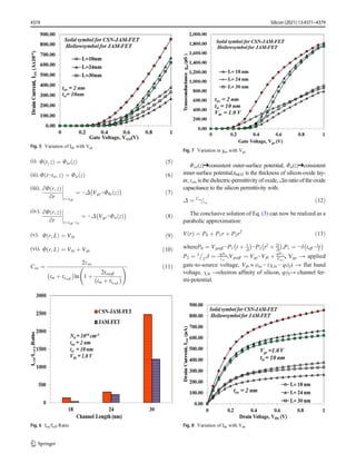
Figure 5 shows the drift in Ids with Vgs for CSN-JAM- FET
and NW-JAM- FET for different channel lengths. Figure 5.
administers that CSN-JAM- FET poses higher Ids over JAM-
FET. This higher change in the drain current owes to the core
shell nanotube FET structure which has two gates. This po-
tential elevates the lateral electric field [26, 27] and also the
gate transport efficiency, thereby enhancing the drain current.
Figure 6 pictures Ratio of ION/IOFF for the contemplated
device designs under channel lengths. Efficiently working as
a switch becomes an essential requisite for a device to be used
for digital applications, thereby making the switching speed a
crucial benchmark It can be expressed [28] as:
ION
IOFF
¼
Ids ON
ð Þat Vgs¼1:0V
Ids OFF
ð Þat Vgs¼0:0V
ð18Þ
As seen from the Fig. 8, the shift in ION/IOFF Ratio is higher
in CSN-JAM- FET over JAM- FET because of superior con-
trol along the channel. Implied from Fig. 7, DMJN-TFET,
solicits grander ION/IOFF ratio because of sharpened adminis-
tration on the channel, crediting tube structure and Dual-Metal
device design. Thus, CSN-JAM- FET(proposed device)
Fig 12 Variation of DIBL with Channel Length
Fig 11 SS v/s Channel Length
Fig 13 Variation of Cgg v/s Vgs with different Channel Length
Fig 14 Variation of fT v/s Vgs with different Channel Length
4376 Silicon (2021) 13:4371–4379](https://image.slidesharecdn.com/7-240902094633-211cbca8/85/NWCore-shell-FET-for-high-frequency-applications-6-320.jpg)