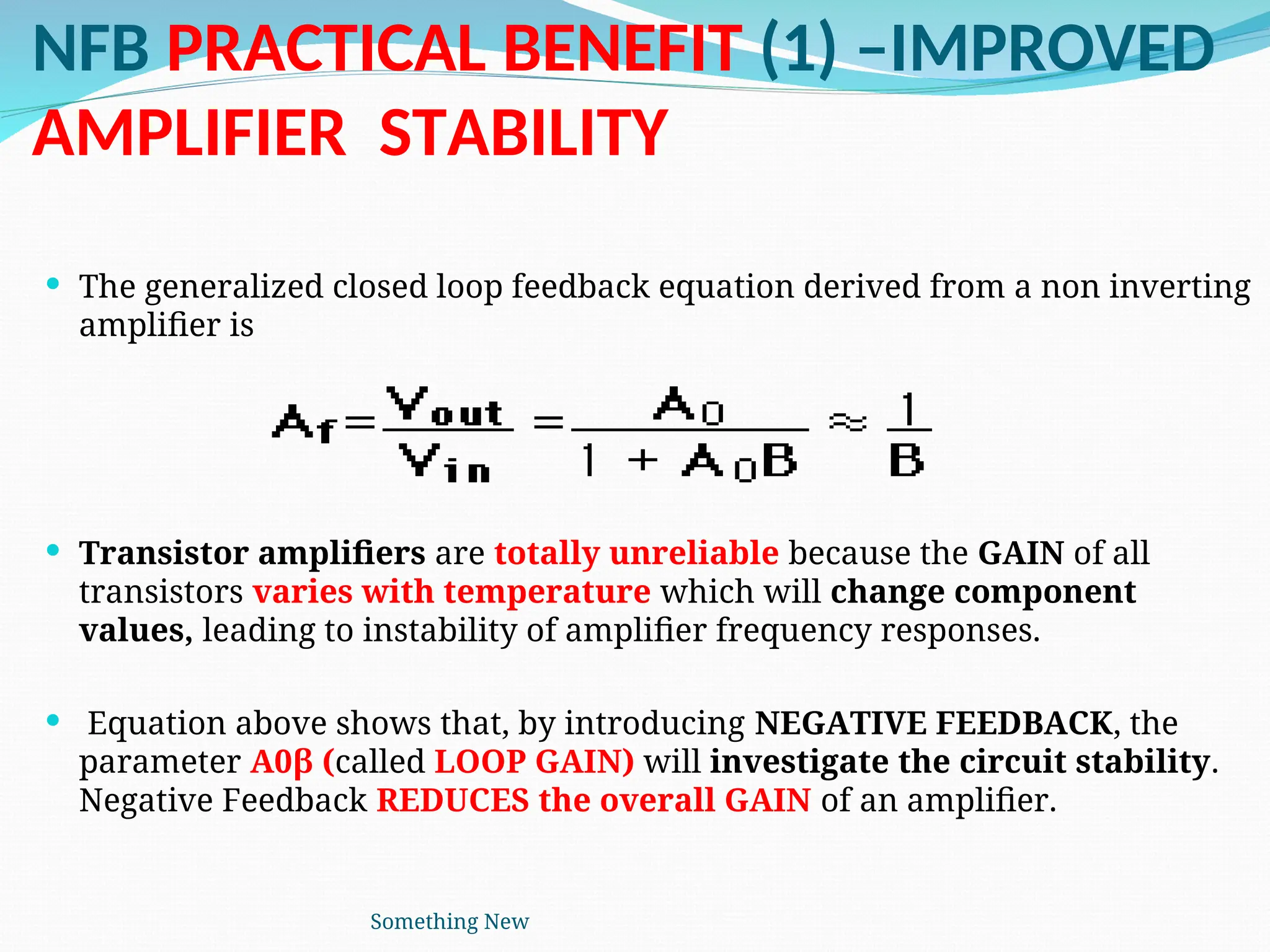
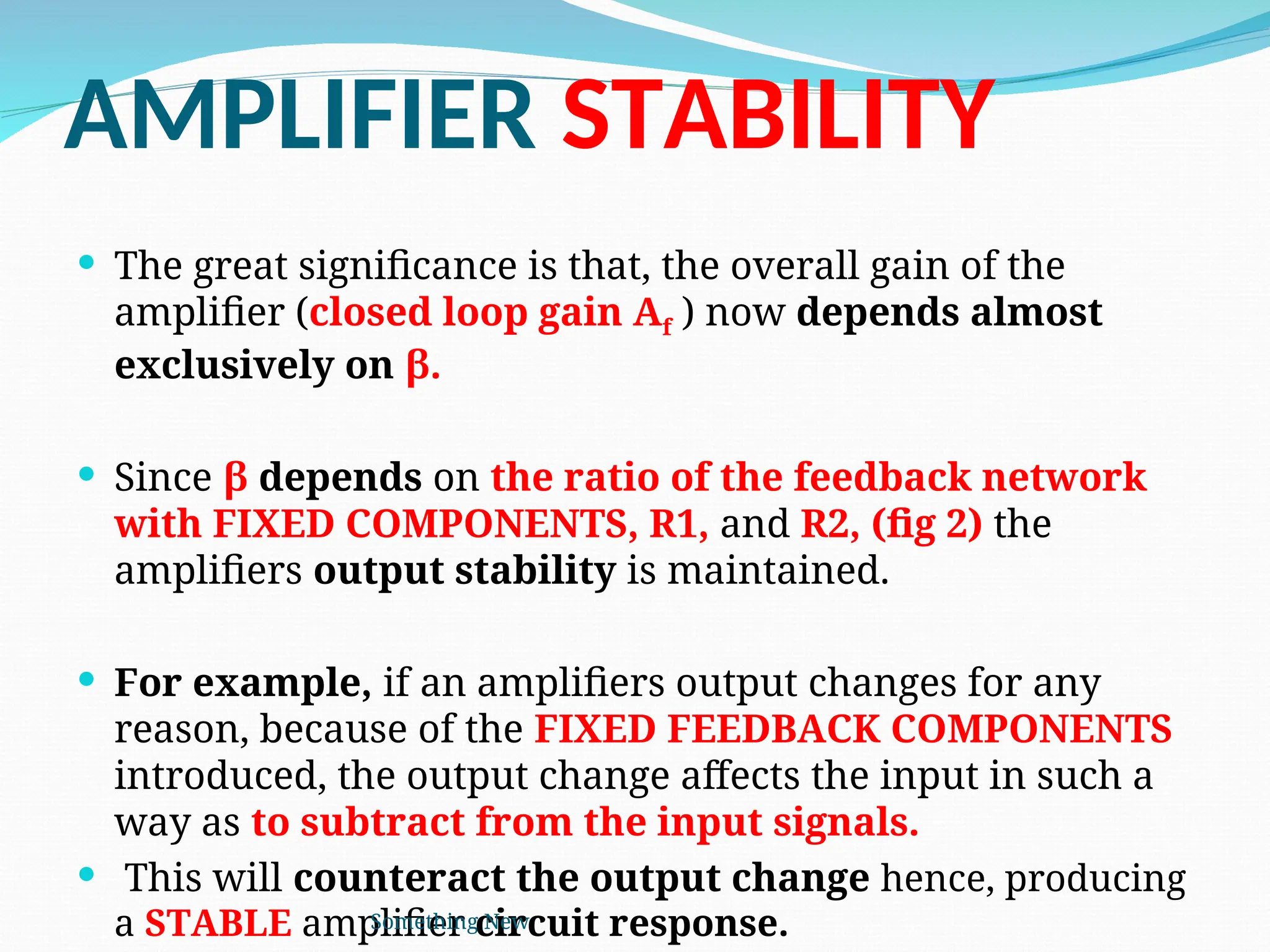
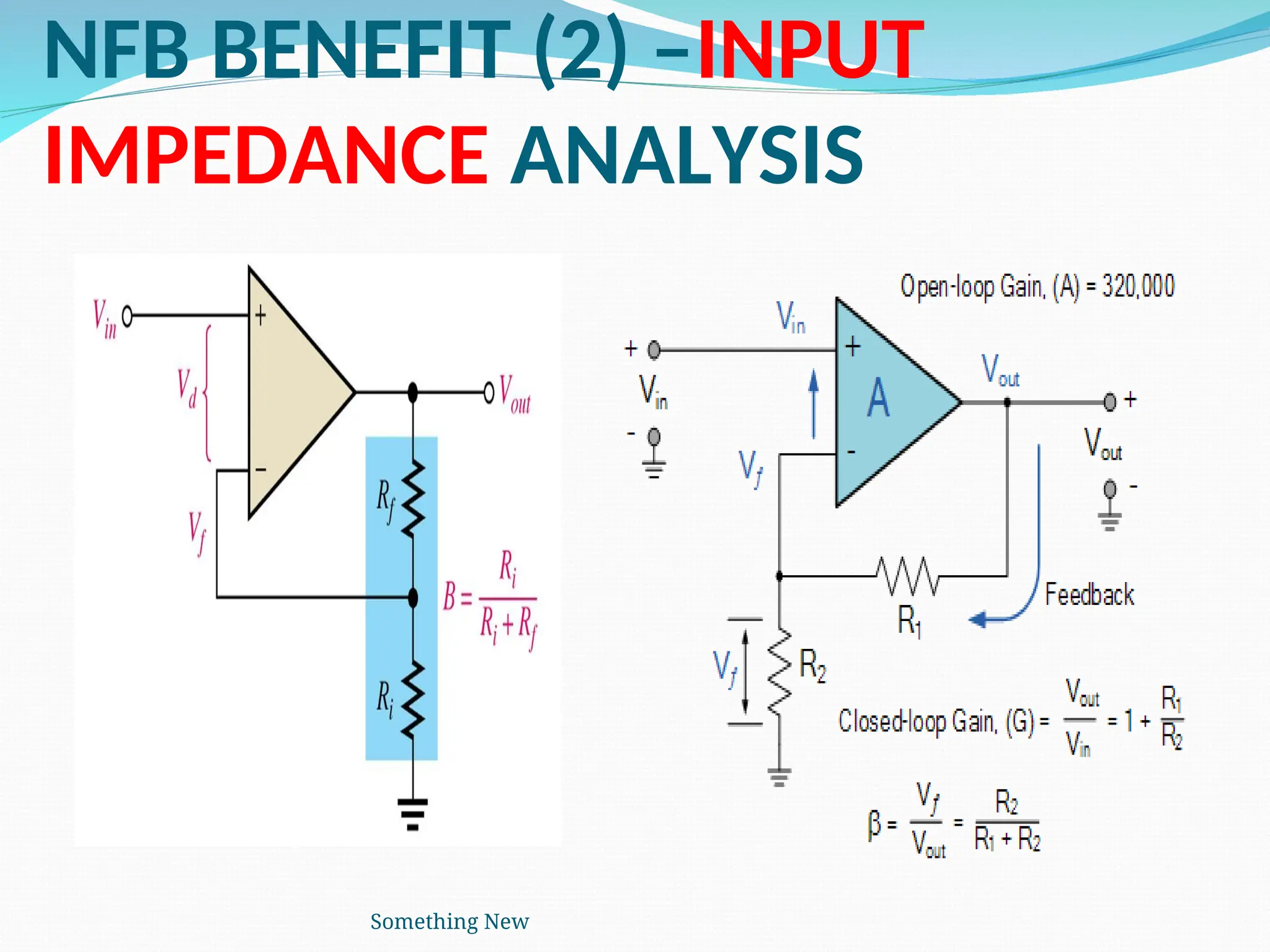
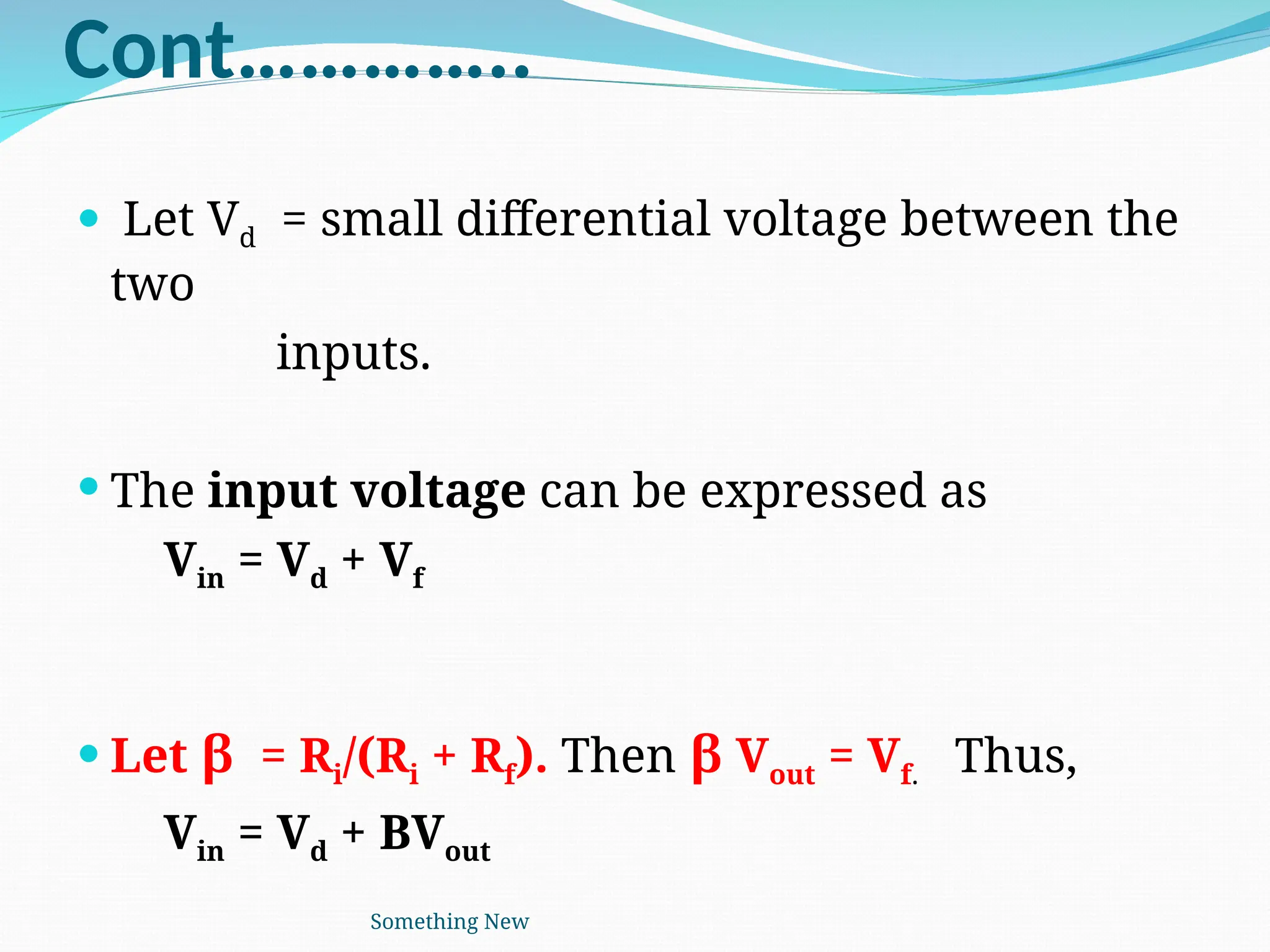
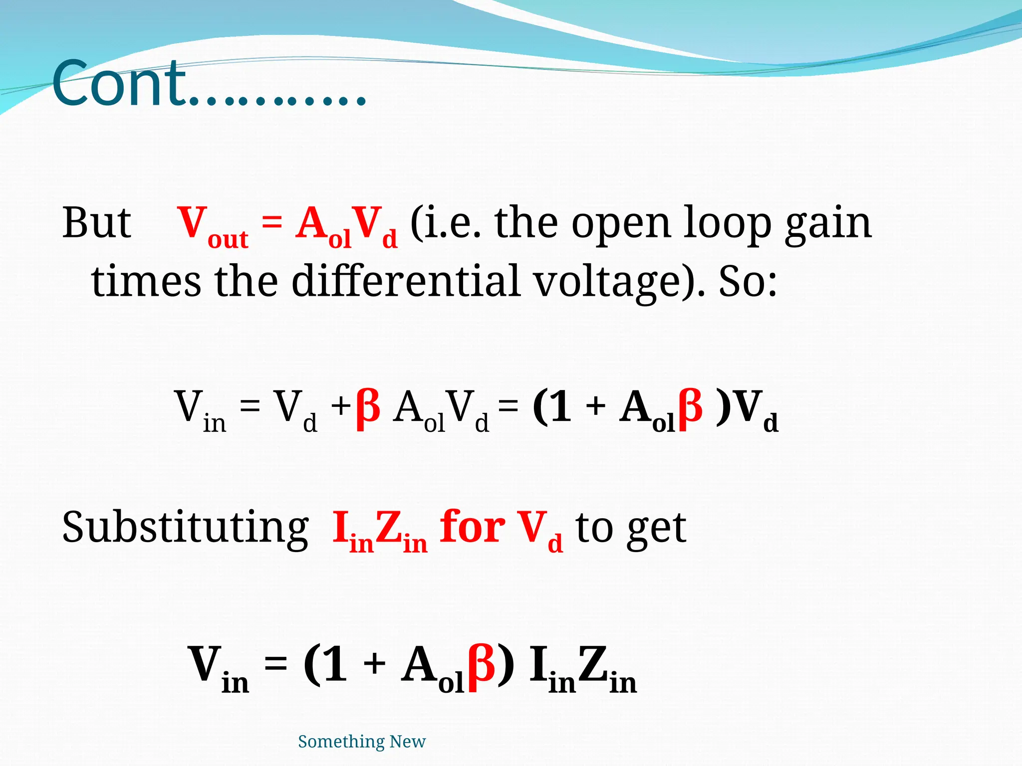
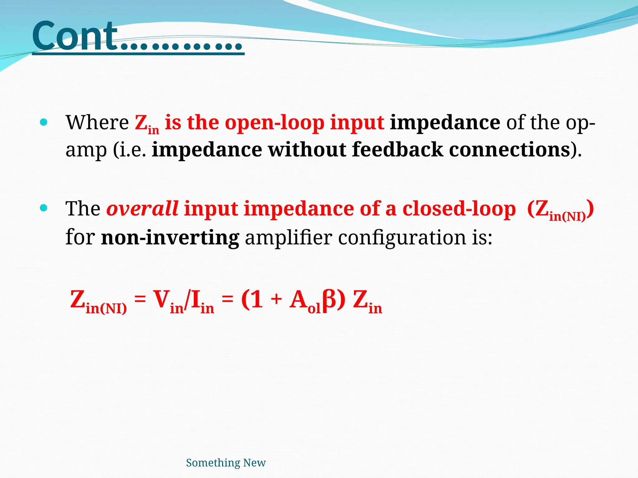
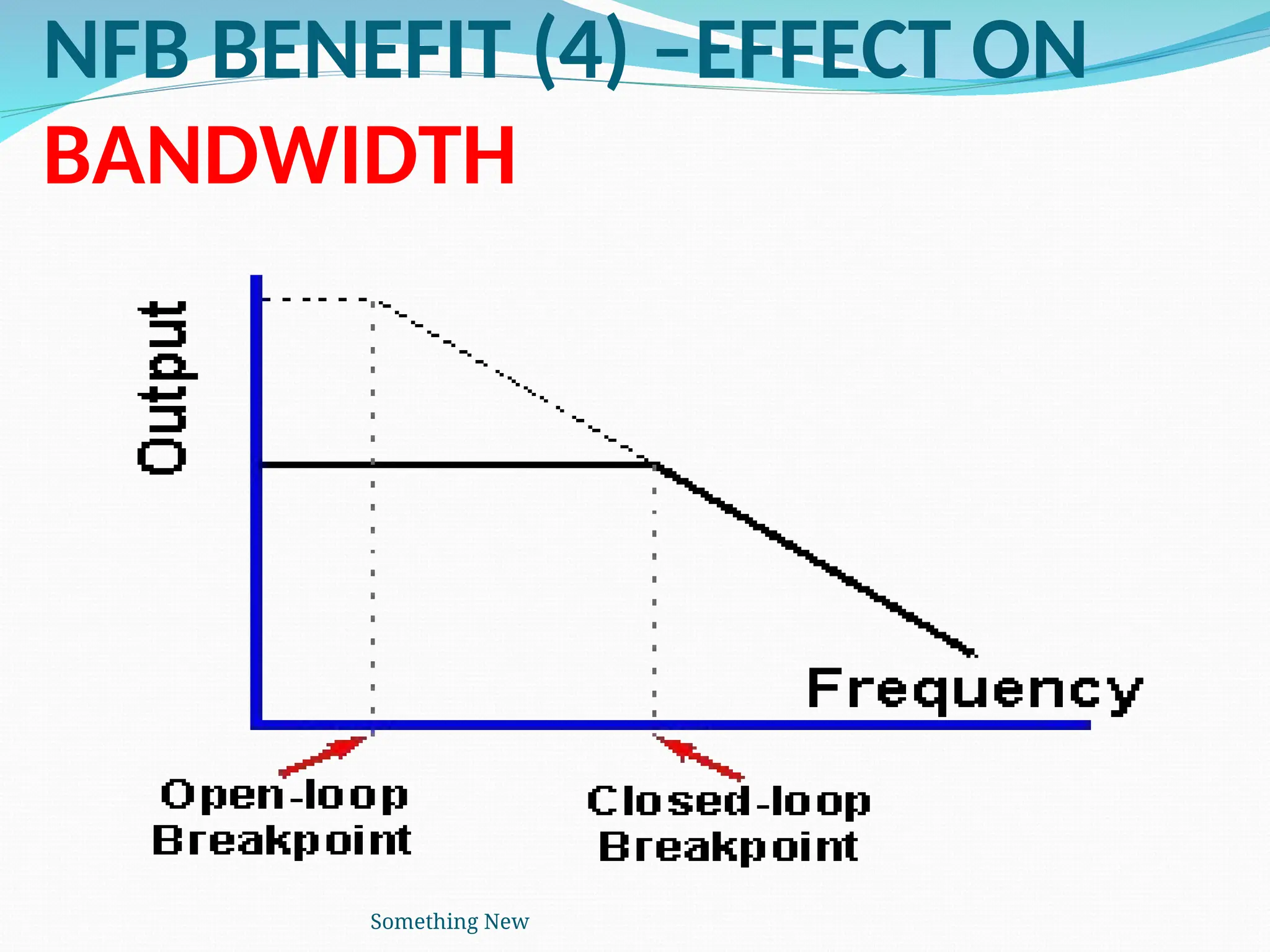
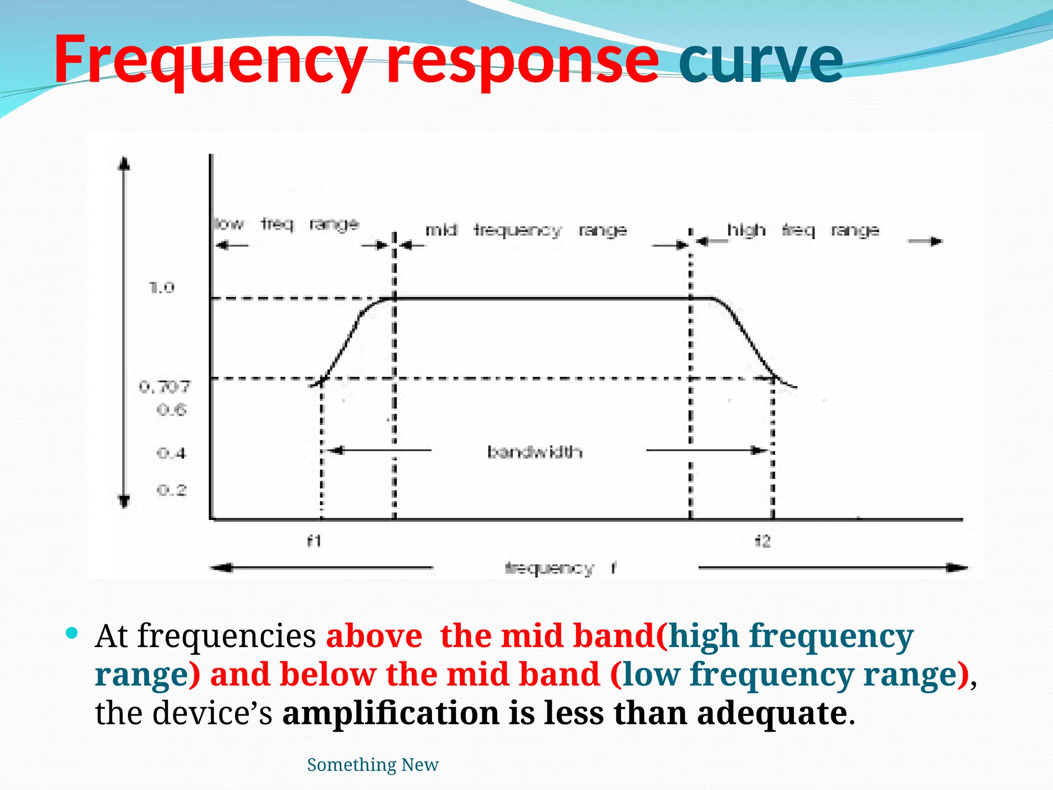
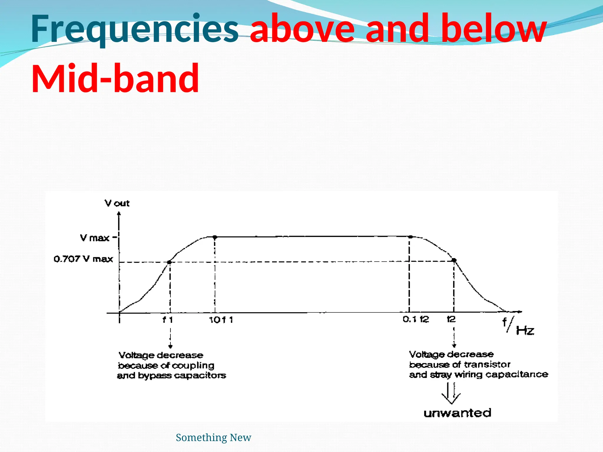
NFB SYSTEMS AND BENEFITS
FIG 1 FIG 2
Something New
BJT AND NFB CONCEPT
Something New
NFB PRACTICAL BENEFIT (1) –IMPROVED
AMPLIFIER STABILITY
 The generalized closed loop feedback equation derived from a non inverting
amplifier is
 Transistor amplifiers are totally unreliable because the GAIN of all
transistors varies with temperature which will change component
values, leading to instability of amplifier frequency responses.
 Equation above shows that, by introducing NEGATIVE FEEDBACK, the
parameter A0β (called LOOP GAIN) will investigate the circuit stability.
Negative Feedback REDUCES the overall GAIN of an amplifier.
Something New
AMPLIFIER STABILITY
 The great significance is that, the overall gain of the
amplifier (closed loop gain Af ) now depends almost
exclusively on β.
 Since β depends on the ratio of the feedback network
with FIXED COMPONENTS, R1, and R2, (fig 2) the
amplifiers output stability is maintained.
 For example, if an amplifiers output changes for any
reason, because of the FIXED FEEDBACK COMPONENTS
introduced, the output change affects the input in such a
way as to subtract from the input signals.
 This will counteract the output change hence, producing
a STABLE amplifier circuit response.
Something New
NFB BENEFIT (2) –INPUT
IMPEDANCE ANALYSIS
Something New
Cont…………..
 Let Vd = small differential voltage between the
two
inputs.
 The input voltage can be expressed as
Vin = Vd + Vf
 Let β = Ri/(Ri + Rf). Then β Vout = Vf. Thus,
Vin = Vd + BVout
Something New
Cont………..
But Vout = AolVd (i.e. the open loop gain
times the differential voltage). So:
Vin = Vd +β AolVd = (1 + Aolβ )Vd
Substituting IinZin for Vd to get
Vin = (1 + Aolβ) IinZin
Something New
Cont…………
 Where Zin is the open-loop input impedance of the op-
amp (i.e. impedance without feedback connections).
 The overall input impedance of a closed-loop (Zin(NI))
for non-inverting amplifier configuration is:
Zin(NI) = Vin/Iin = (1 + Aolβ) Zin
Something New
Benefit ONE:
Effect on Input Impedance
Equation 1 shows that, the input
impedance of an amplifier with
negative feedback is much
greater than (INCREASED) the
internal input impedance of the op-
amp itself (i.e. without feedback
Something New
NFB BENEFIT (3) –OUTPUT
IMPEDANCE ANALYSIS
Something New
Cont…………
Apply Kirchhoff’s law to the output circuit to
get:
 Vout = AolVd – ZoutIout
 The differential input is Vd = Vin – Vf.
Assume AolVd >> ZoutIout. Then,
 Vout = Aol(Vin – Vf)
 The differential input is Vd = Vin – Vf.
 Assume AolVd >> ZoutIout. Then,
 Vout = Aol(Vin – Vf)
Something New
Cont……….
 Let β = B. Substitute BVout­for Vf to get
 Vout = Aol(Vin – BVout) = AolVin – AolBVout
 AolVin = Vout + AolBVout = (1 + AolB)Vout
 The output impedance of the non-inverting amplifier
is Zout(NI) = Vout/Iout.
 Substitute IoutZout(NI) for Vout:
 AolVin = (1 + AolB) IoutZout(NI)
Something New
Cont………
OR….
 AolVin/Iout = (1 + AolB) Zout(NI)
Without feedback, AolVin = Vout. Thus,
 Zout = (1 + AolB) Zout(NI)
With Feedback
Zout(NI) = Zout / (1 + AolB)
Something New
Benefit Three:
Effect on Output impedance
Thus the output impedance of an
amplifier with negative
feedback is much less
(DECREASED) than the internal
output impedance, Zout, of the op-
amp itself( i.e. without feedback).
Something New
NFB BENEFIT (4) –EFFECT ON
BANDWIDTH
Something New
EFFECT ON BANDWIDTH
 Typically Op Amps are used for comparatively low
frequency circuits. But for improved performance,
negative feedback could be employed.
 Negative Feedback is used to INCREASE the
BANDWIDTH of an amplifier (speed it up) at the cost of
lowering the amplifier gain
 Thus, the stabilization of gain increases the effective
bandwidth. It flattens and extends the frequency response
of an amplifier.
 Negative Feedback is a major contribution to extending the
useful frequency range of amplifiers.
Something New
What is Frequency Response
 Some components of an amplifier have frequency limitations
and so respond differently as the frequency changes.
 Since the response of components varies with the frequency,
the components of an amplifier must be selected to amplify a
certain range or band of frequencies.
 Hence, how well (i.e. linearity) an amplifier will perform
without attenuation is described by frequency response.
 The frequency response of an amplifier refers to the frequency
range that the amplifier is designed to amplify. A High
Fidelity amplifier must exhibit a flat response from 20Hz –
20kHz
Something New
Cont……….
 The frequency range in which the amplifier will
operate with negligible effects from capacitors,
inductors, and device internal capacitance is called
Mid-Frequency Range or Mid Band Frequency.
 Bandwidth refers to the ‘band’ of frequencies for
which the amplifier provides adequate amplification.
 Bandwidth is normally measured at the 3dB point (s)
of the frequency response.
 3dB is the frequency at which the output signal is
cutoff to 70.7% of the input signal value.
Something New
Plotting Frequency Response Curve
 A frequency-response curve is a graphical representation of
the relationship between amplifier gain and operating
frequency.
 In such graphs, Gain is plotted against Frequency. It is
common that very large values may be encountered for both
gain and frequency. To ensure that wide range of values
are plotted on a single graph both the frequency and gain
axes of the graph may use logarithmic scales.
 The (vertical) y-axis uses linear divisions or logarithmic units
in (decibels dB).
 The (horizontal) x-axis is a frequency scale which has a large
range of quantities and so does not increase in a linear
manner. For this reason it uses the logarithmic scale.
Something New
Graphical Representation of
Frequency Response Curve
The curve shows how gain, measured in deciBels (dB)
varies with frequency.
Something New
Frequency response curve
 At frequencies above the mid band(high frequency
range) and below the mid band (low frequency range),
the device’s amplification is less than adequate.
Something New
Frequencies above and below
Mid-band
Something New
Frequency Response….cont
 All transistors show less gain as the frequency
increases. WHY ?
 The high frequency limit for a transistor is related
to the junction capacitances called MILLER
EFFECT named after JOHN MILTON MILLER.
 Miller Effect is the effect of a larger capacitance
introduced between the transistor’s base (in BJTs)
or gate (in FETs) and its collector or drain, which
LIMITS a transistor’s GAIN at HIGH
FREQUENCIES.
Something New
MILLER EFFECT
 Note that Vcc is +
 The collector-base capacit
 ance CCB and emitter-base
 capacitance CEB decrease
 the gain of a common emitter
 circuit at higher frequencies.
 The Miller effect makes Ccb
look β times larger at the base
 of a CE amplifier.
 The reactance of a capacitor decreases as the frequency
increases. This decreasing reactance loads the amplifier,
hence dropping the gain.
Something New
TRANSISTORS GAIN AND
FREQUENCY VARIATIONS
Why all transistors show LESS GAIN as FREQUENCY
DECREASES or INCREASES.
 At frequencies above and below the midrange,
capacitance and any inductance will affect the gain of the
amplifier.
 At low frequencies the coupling and bypass capacitors
lower the gain.
 At high frequencies stray capacitances associated with the
active device lower the gain.
Something New
BENEFIT FIVE: NFB EFFECT ON
AMPLIFIER DISTORTION
Due to the parameters of a signal, the process of amplification
introduces some DISTORTIONS. Reactive components in
amplifiers will introduce frequency and phase distortions, while
Amplitude distortion is mostly caused by poor DC biasing.
 Distortion in amplifiers is ANY CHANGE in the BASIC NATURE of
an input signal waveform.
 The use of negative feedback can discriminate against sources of
distortion within an amplifier.
 Thus, Negative Feedback REDUCES DISTORTION generated in the
stages of an amplifier.
 Introducing Negative feedback to reduce distortion will
IMPROVE the FIDELITY of an amplifier by reproducing the EXACT
NATURE of the input signal at the output stage.
Something New
NOISE IN AMPLIFIERS
External Generated
 Occurs across the whole bandwidth or frequency
spectrum of an amplifier
 May come from entirely natural sources such ‘static’
noise in the form of hissing and cracking radiated from
space
 Atmospheric noise generated by lightning discharges
in thunderclouds.
 Transmissions broadcasting at similar frequencies to
the required signal.
Something New
NOISE IN AMPLIFIERS
 All signals are contaminated with noise as unwanted sound.
 Internally Generated
 Resistors, Transistors, especially bipolar types, will generate
noise from a variety of causes including Thermal noise caused
by heat.
 Shot noise’, which is caused by charge carriers (electrons and
holes) randomly diffusing across the semiconductor junctions.
 Flicker Noise which is found in all semiconductor devices
under the application of a current bias.
 Avalanche Noise- caused by Zener or avalanche
breakdown in a pn junction
Something New
BENEFIT SIX: NFB EFFECT ON
NOISE
 Noise at frequencies above and below the
required bandwidth of the amplifier can be
REDUCED by Negative Feedback using high
and low pass filters.
 Negative feedback can play a part in
improving the signal to noise ratio within
the bandwidth of an amplifier.
Something New
WAAAAAAOOOOOOOOOO
END
Something New

NFB SYSTEMS AND BENEFITS ELECTRONICS III- L2- Jan 2020.ppt

  • 1.
    NFB SYSTEMS ANDBENEFITS FIG 1 FIG 2 Something New
  • 2.
    BJT AND NFBCONCEPT Something New
  • 3.
    NFB PRACTICAL BENEFIT(1) –IMPROVED AMPLIFIER STABILITY  The generalized closed loop feedback equation derived from a non inverting amplifier is  Transistor amplifiers are totally unreliable because the GAIN of all transistors varies with temperature which will change component values, leading to instability of amplifier frequency responses.  Equation above shows that, by introducing NEGATIVE FEEDBACK, the parameter A0β (called LOOP GAIN) will investigate the circuit stability. Negative Feedback REDUCES the overall GAIN of an amplifier. Something New
  • 4.
    AMPLIFIER STABILITY  Thegreat significance is that, the overall gain of the amplifier (closed loop gain Af ) now depends almost exclusively on β.  Since β depends on the ratio of the feedback network with FIXED COMPONENTS, R1, and R2, (fig 2) the amplifiers output stability is maintained.  For example, if an amplifiers output changes for any reason, because of the FIXED FEEDBACK COMPONENTS introduced, the output change affects the input in such a way as to subtract from the input signals.  This will counteract the output change hence, producing a STABLE amplifier circuit response. Something New
  • 5.
    NFB BENEFIT (2)–INPUT IMPEDANCE ANALYSIS Something New
  • 6.
    Cont…………..  Let Vd= small differential voltage between the two inputs.  The input voltage can be expressed as Vin = Vd + Vf  Let β = Ri/(Ri + Rf). Then β Vout = Vf. Thus, Vin = Vd + BVout Something New
  • 7.
    Cont……….. But Vout =AolVd (i.e. the open loop gain times the differential voltage). So: Vin = Vd +β AolVd = (1 + Aolβ )Vd Substituting IinZin for Vd to get Vin = (1 + Aolβ) IinZin Something New
  • 8.
    Cont…………  Where Zinis the open-loop input impedance of the op- amp (i.e. impedance without feedback connections).  The overall input impedance of a closed-loop (Zin(NI)) for non-inverting amplifier configuration is: Zin(NI) = Vin/Iin = (1 + Aolβ) Zin Something New
  • 9.
    Benefit ONE: Effect onInput Impedance Equation 1 shows that, the input impedance of an amplifier with negative feedback is much greater than (INCREASED) the internal input impedance of the op- amp itself (i.e. without feedback Something New
  • 10.
    NFB BENEFIT (3)–OUTPUT IMPEDANCE ANALYSIS Something New
  • 11.
    Cont………… Apply Kirchhoff’s lawto the output circuit to get:  Vout = AolVd – ZoutIout  The differential input is Vd = Vin – Vf. Assume AolVd >> ZoutIout. Then,  Vout = Aol(Vin – Vf)  The differential input is Vd = Vin – Vf.  Assume AolVd >> ZoutIout. Then,  Vout = Aol(Vin – Vf) Something New
  • 12.
    Cont……….  Let β= B. Substitute BVout­for Vf to get  Vout = Aol(Vin – BVout) = AolVin – AolBVout  AolVin = Vout + AolBVout = (1 + AolB)Vout  The output impedance of the non-inverting amplifier is Zout(NI) = Vout/Iout.  Substitute IoutZout(NI) for Vout:  AolVin = (1 + AolB) IoutZout(NI) Something New
  • 13.
    Cont……… OR….  AolVin/Iout =(1 + AolB) Zout(NI) Without feedback, AolVin = Vout. Thus,  Zout = (1 + AolB) Zout(NI) With Feedback Zout(NI) = Zout / (1 + AolB) Something New
  • 14.
    Benefit Three: Effect onOutput impedance Thus the output impedance of an amplifier with negative feedback is much less (DECREASED) than the internal output impedance, Zout, of the op- amp itself( i.e. without feedback). Something New
  • 15.
    NFB BENEFIT (4)–EFFECT ON BANDWIDTH Something New
  • 16.
    EFFECT ON BANDWIDTH Typically Op Amps are used for comparatively low frequency circuits. But for improved performance, negative feedback could be employed.  Negative Feedback is used to INCREASE the BANDWIDTH of an amplifier (speed it up) at the cost of lowering the amplifier gain  Thus, the stabilization of gain increases the effective bandwidth. It flattens and extends the frequency response of an amplifier.  Negative Feedback is a major contribution to extending the useful frequency range of amplifiers. Something New
  • 17.
    What is FrequencyResponse  Some components of an amplifier have frequency limitations and so respond differently as the frequency changes.  Since the response of components varies with the frequency, the components of an amplifier must be selected to amplify a certain range or band of frequencies.  Hence, how well (i.e. linearity) an amplifier will perform without attenuation is described by frequency response.  The frequency response of an amplifier refers to the frequency range that the amplifier is designed to amplify. A High Fidelity amplifier must exhibit a flat response from 20Hz – 20kHz Something New
  • 18.
    Cont……….  The frequencyrange in which the amplifier will operate with negligible effects from capacitors, inductors, and device internal capacitance is called Mid-Frequency Range or Mid Band Frequency.  Bandwidth refers to the ‘band’ of frequencies for which the amplifier provides adequate amplification.  Bandwidth is normally measured at the 3dB point (s) of the frequency response.  3dB is the frequency at which the output signal is cutoff to 70.7% of the input signal value. Something New
  • 19.
    Plotting Frequency ResponseCurve  A frequency-response curve is a graphical representation of the relationship between amplifier gain and operating frequency.  In such graphs, Gain is plotted against Frequency. It is common that very large values may be encountered for both gain and frequency. To ensure that wide range of values are plotted on a single graph both the frequency and gain axes of the graph may use logarithmic scales.  The (vertical) y-axis uses linear divisions or logarithmic units in (decibels dB).  The (horizontal) x-axis is a frequency scale which has a large range of quantities and so does not increase in a linear manner. For this reason it uses the logarithmic scale. Something New
  • 20.
    Graphical Representation of FrequencyResponse Curve The curve shows how gain, measured in deciBels (dB) varies with frequency. Something New
  • 21.
    Frequency response curve At frequencies above the mid band(high frequency range) and below the mid band (low frequency range), the device’s amplification is less than adequate. Something New
  • 22.
    Frequencies above andbelow Mid-band Something New
  • 23.
    Frequency Response….cont  Alltransistors show less gain as the frequency increases. WHY ?  The high frequency limit for a transistor is related to the junction capacitances called MILLER EFFECT named after JOHN MILTON MILLER.  Miller Effect is the effect of a larger capacitance introduced between the transistor’s base (in BJTs) or gate (in FETs) and its collector or drain, which LIMITS a transistor’s GAIN at HIGH FREQUENCIES. Something New
  • 24.
    MILLER EFFECT  Notethat Vcc is +  The collector-base capacit  ance CCB and emitter-base  capacitance CEB decrease  the gain of a common emitter  circuit at higher frequencies.  The Miller effect makes Ccb look β times larger at the base  of a CE amplifier.  The reactance of a capacitor decreases as the frequency increases. This decreasing reactance loads the amplifier, hence dropping the gain. Something New
  • 25.
    TRANSISTORS GAIN AND FREQUENCYVARIATIONS Why all transistors show LESS GAIN as FREQUENCY DECREASES or INCREASES.  At frequencies above and below the midrange, capacitance and any inductance will affect the gain of the amplifier.  At low frequencies the coupling and bypass capacitors lower the gain.  At high frequencies stray capacitances associated with the active device lower the gain. Something New
  • 26.
    BENEFIT FIVE: NFBEFFECT ON AMPLIFIER DISTORTION Due to the parameters of a signal, the process of amplification introduces some DISTORTIONS. Reactive components in amplifiers will introduce frequency and phase distortions, while Amplitude distortion is mostly caused by poor DC biasing.  Distortion in amplifiers is ANY CHANGE in the BASIC NATURE of an input signal waveform.  The use of negative feedback can discriminate against sources of distortion within an amplifier.  Thus, Negative Feedback REDUCES DISTORTION generated in the stages of an amplifier.  Introducing Negative feedback to reduce distortion will IMPROVE the FIDELITY of an amplifier by reproducing the EXACT NATURE of the input signal at the output stage. Something New
  • 27.
    NOISE IN AMPLIFIERS ExternalGenerated  Occurs across the whole bandwidth or frequency spectrum of an amplifier  May come from entirely natural sources such ‘static’ noise in the form of hissing and cracking radiated from space  Atmospheric noise generated by lightning discharges in thunderclouds.  Transmissions broadcasting at similar frequencies to the required signal. Something New
  • 28.
    NOISE IN AMPLIFIERS All signals are contaminated with noise as unwanted sound.  Internally Generated  Resistors, Transistors, especially bipolar types, will generate noise from a variety of causes including Thermal noise caused by heat.  Shot noise’, which is caused by charge carriers (electrons and holes) randomly diffusing across the semiconductor junctions.  Flicker Noise which is found in all semiconductor devices under the application of a current bias.  Avalanche Noise- caused by Zener or avalanche breakdown in a pn junction Something New
  • 29.
    BENEFIT SIX: NFBEFFECT ON NOISE  Noise at frequencies above and below the required bandwidth of the amplifier can be REDUCED by Negative Feedback using high and low pass filters.  Negative feedback can play a part in improving the signal to noise ratio within the bandwidth of an amplifier. Something New
  • 30.