
Recommended
More Related Content
Similar to MEMS capability @ CSEM
Similar to MEMS capability @ CSEM (20)
Recently uploaded
Recently uploaded (20)
MEMS capability @ CSEM
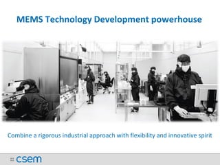
- 1. MEMS Technology Development powerhouse Combine a rigorous industrial approach with flexibility and innovative spirit
- 2. Copyright 2017 CSEM | Micro and Nano Systems | Page 1 • From proof-of-concept studies to small series production • CSEM has a long track record of MEMS projects in multiple industrial domains including: • Watchmaking • Medical • Industrial & Instrumentation • Automotive & Aerospace • Telecommunication • Clean room details: • Newly built and equipped in 2015 • 1200 m² clean room class 100 / ISO5 • Fully dedicated experienced engineering staff • 150 mm wafers & 100mm possible • Wide range of process technologies & materials • First level of packaging • Preferential access to extended MEMS foundry Network MEMS technology development powerhouse Infrastructure - 1
- 3. Copyright 2017 CSEM | Micro and Nano Systems | Page 2 MEMS Process Technology • Photolithography • Thicknesses: 700nm to 50 µm • Resolution: 800nm & stepper • Photolithography SU8 • Thicknesses: 10 to 250 µm • Resolution: 2 µm • Etching • Wet etching KOH, SiO2, Metals, … • Dry etching RIE • Thin film deposition • Metal and metal oxides (sputtering, evaporation, ALD, ..) • Dielectrics (Thermal Oxidation, LPCVD, APCVD, PECVD, MVD, ALD) • Parylene coating • Structural Dry resist lamination • N-type / P-type junctions / Ion implants Standard processes Special processes • Deep-RIE • Depth up to 700µm / Verticality: < 0.1° • Silicon Carbide • Wafer level bonding • Anodic, fusion, eutectic • Piezo Thin Film (AlN, AlScN, PZT, …) • Galvanic processes (Au, Ni, NiP, Cu, ..) • Electroless metal deposition • Diamond & Diamond-Like Carbon deposition • Precise Diamond Machining • Laser cutting • SACE – Glass wafer patterning • SEM / TEM / FIB / HD-XRD Failure mode and reliability analysis Infrastructure - 1
- 4. Copyright 2017 CSEM | Micro and Nano Systems | Page 3 MEMS development cycle • CSEM can handle very complex projects from conceptual phase to system integration, from component to application with emphasis on watch components, gas sensors, micro mirrors, inertial sensors, pressure sensors, bio-interacting & optical microsystems With its unique experience in high end MEMS products and system know- how … Design & Simulation Foundry Technology services Wafer processing Engineering & production scale-up Testing electrical, mechanical & Characterization microscopy, spectroscopy, X-ray diffraction Packaging Feasibility to small series, industrialization processes & development
- 5. Copyright 2017 CSEM | Micro and Nano Systems | Page 4 Quality system • ISO 9001:2008 certified • ISO 13485 capable • Library of technological blocks • Electronic lot documentation and WIP (CFAB) • Process flow and lot traveler • Lot tracking • Wafer stock • Industrial cost model • Rush lot with expedited turn-around time MEMS process technology
- 6. Thank You !
- 7. Thank you for your attention and follow us on www.csem.ch ̶ ̶ ̶ ̶ ̶ ̶ ̶ ̶ ̶ ̶ ̶ ̶ ̶ ̶ ̶ ̶ ̶ ̶ ̶ ̶ ̶ ̶ ̶ ̶ ̶ ̶ ̶ ̶ ̶ ̶ ̶ ̶ ̶ ̶ ̶ ̶ ̶ ̶ ̶ ̶ ̶ ̶ ̶ ̶ ̶ ̶ ̶ ̶ ̶ ̶ ̶ ̶ ̶ ̶ ̶ ̶ ̶ ̶ ̶ ̶ ̶ ̶ ̶ Michele Palmieri Vice President, Micro & Nano Systems Division michele.palmieri@csem.ch M +41 78 936 6309 ¦ T +41 32 720 5045 ̶ ̶ ̶ ̶ ̶ ̶ ̶ ̶ ̶ ̶ ̶ ̶ ̶ ̶ ̶ ̶ ̶ ̶ ̶ ̶ ̶ ̶ ̶ ̶ ̶ ̶ ̶ ̶ ̶ ̶ ̶ ̶ ̶ ̶ ̶ ̶ ̶ ̶ ̶ ̶ ̶ ̶ ̶ ̶ ̶ ̶ ̶ ̶ ̶ ̶ ̶ ̶ ̶ ̶ ̶ ̶ ̶ ̶ ̶ ̶ ̶ ̶ ̶