Dr. Allam Ameen
AssistantProfessor
Egyptian Chinese University, Faculty of Engineering and Technology
Electronics Research Institute, Microstrip Department
Lecture 3
Spring 2025
Electronic Circuits
(MCT 123)
2.
Last Lecture Topics
Dr.Allam Ameen Electronic Circuits
2
PN Junction.
Applications of PN Junction.
Diode.
Biasing of the Diode.
Diode Models.
V-I Characteristic of a Diode.
3.
Today’s Topics
Dr. AllamAmeen Electronic Circuits
3
Half-Wave Rectifiers.
Full-Wave Rectifiers.
Power Supply Filters.
Diode Limiters.
Diode Clippers.
Diode Clampers.
Completed Power Supply.
4.
Full-Wave Rectifiers
Dr. AllamAmeen Electronic Circuits
4
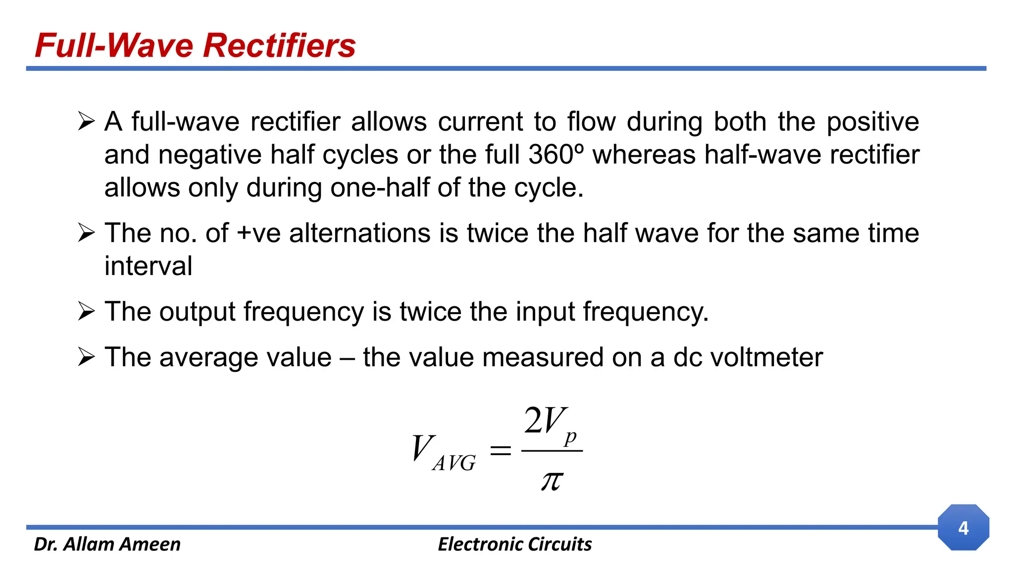
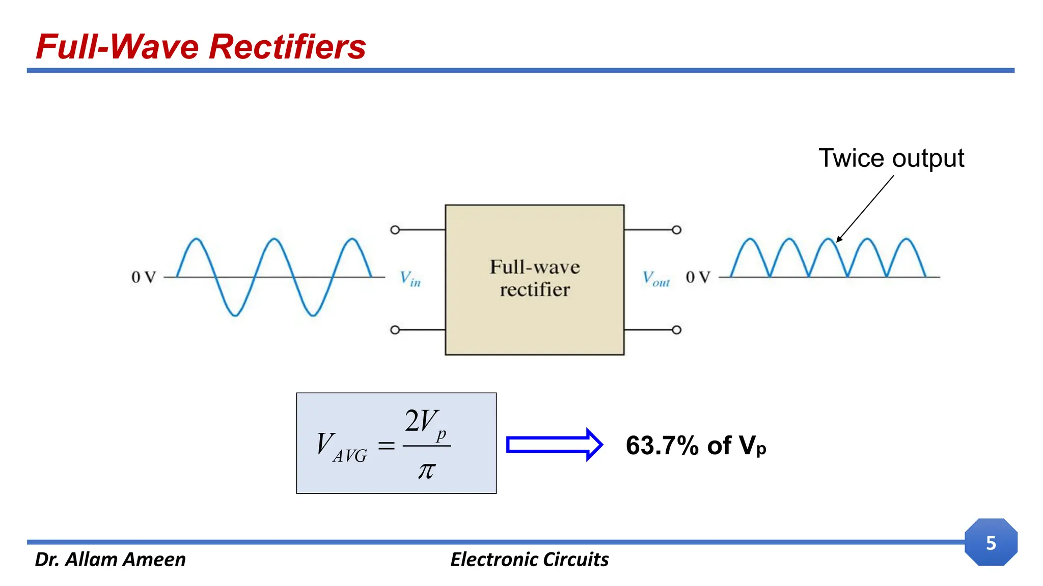
A full-wave rectifier allows current to flow during both the positive
and negative half cycles or the full 360º whereas half-wave rectifier
allows only during one-half of the cycle.
The no. of +ve alternations is twice the half wave for the same time
interval
The output frequency is twice the input frequency.
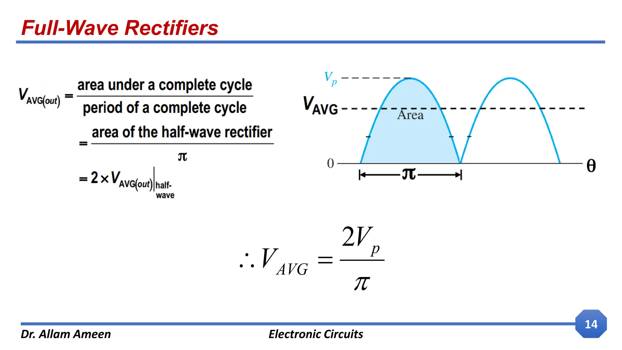
The average value – the value measured on a dc voltmeter
p
AVG
V
V
2
Full-Wave Rectifiers
Dr. AllamAmeen Electronic Circuits
6
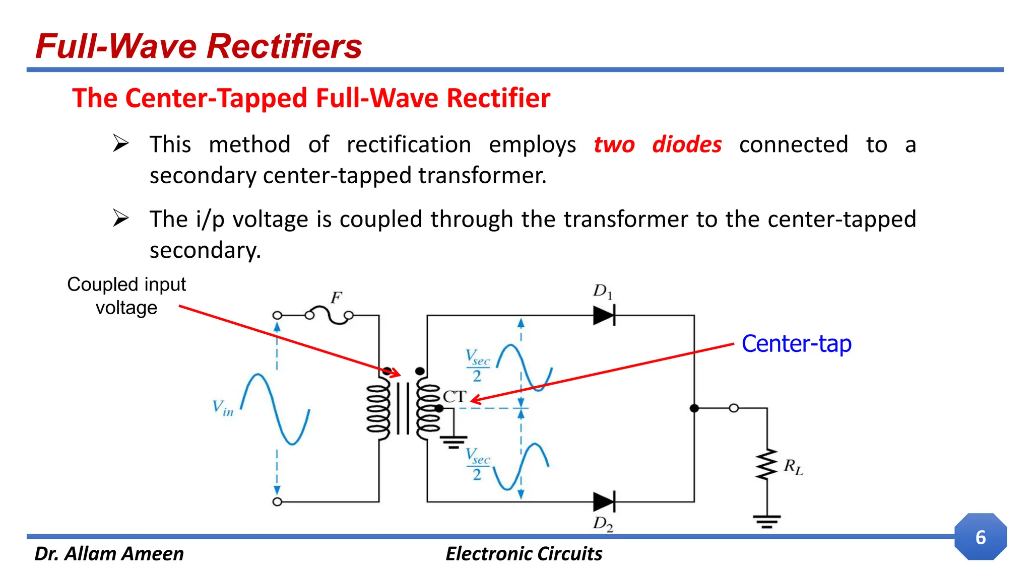
The Center-Tapped Full-Wave Rectifier
This method of rectification employs two diodes connected to a
secondary center-tapped transformer.
The i/p voltage is coupled through the transformer to the center-tapped
secondary.
Coupled input
voltage
Center-tap
7.
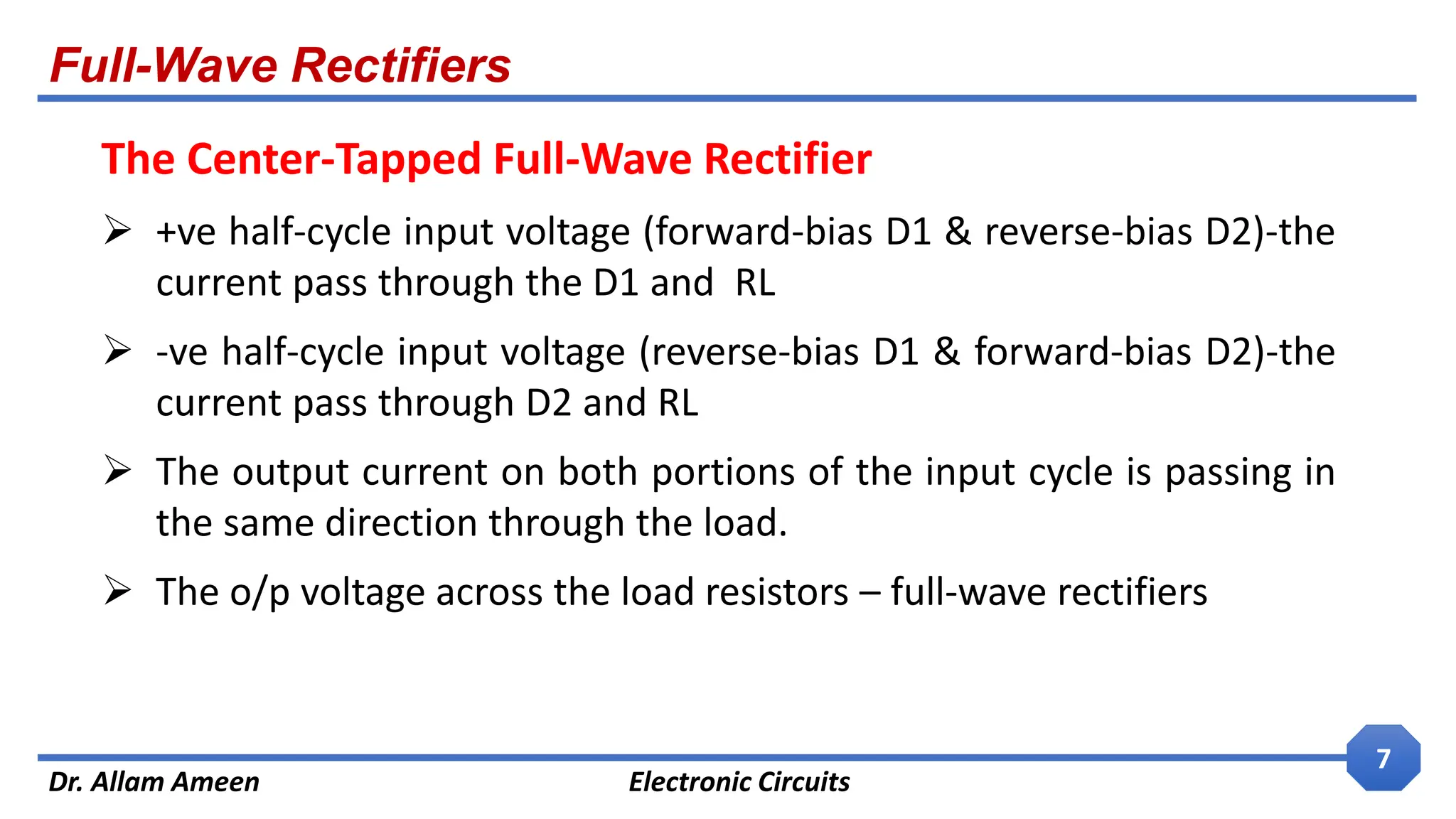
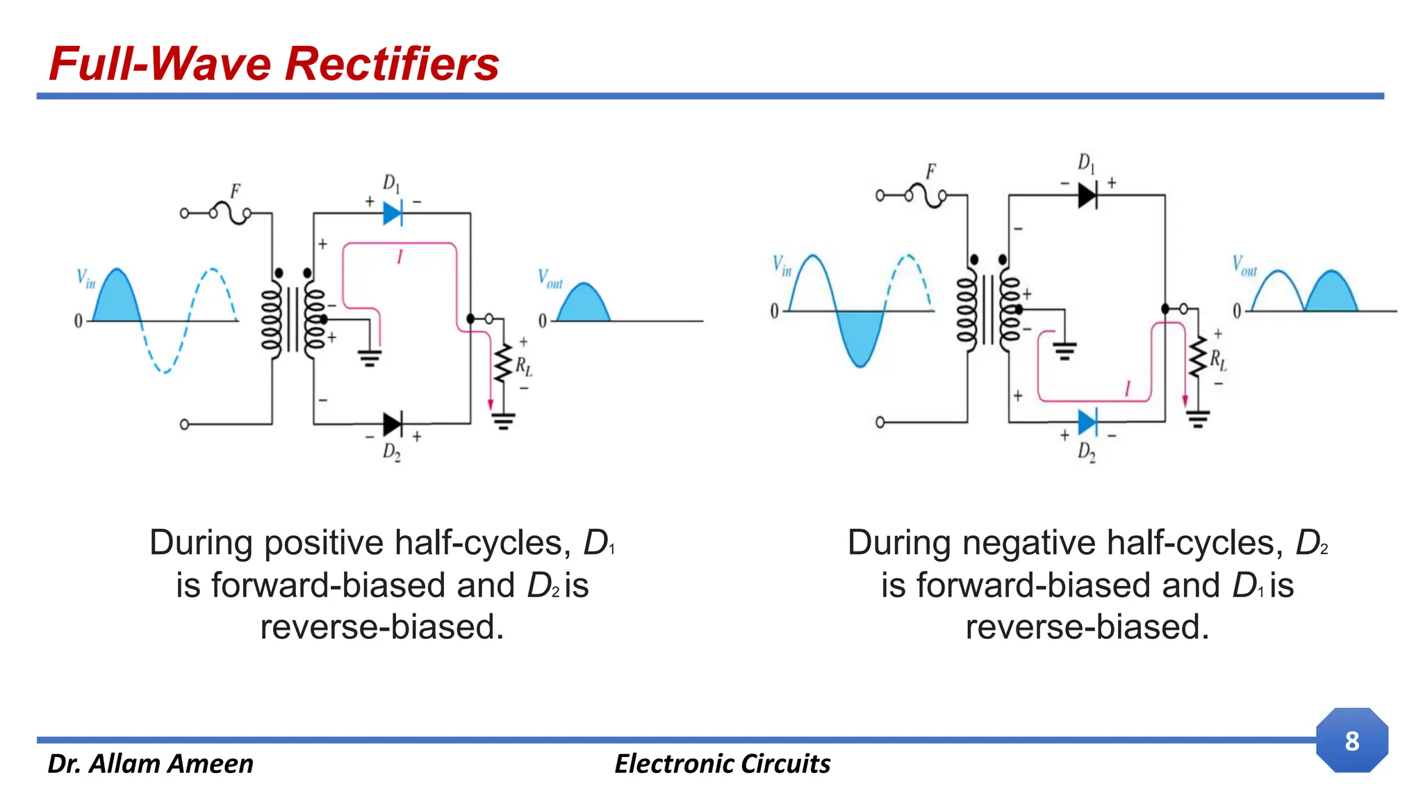
Full-Wave Rectifiers
Dr. AllamAmeen Electronic Circuits
7
The Center-Tapped Full-Wave Rectifier
+ve half-cycle input voltage (forward-bias D1 & reverse-bias D2)-the
current pass through the D1 and RL
-ve half-cycle input voltage (reverse-bias D1 & forward-bias D2)-the
current pass through D2 and RL
The output current on both portions of the input cycle is passing in
the same direction through the load.
The o/p voltage across the load resistors – full-wave rectifiers
8.
Full-Wave Rectifiers
Dr. AllamAmeen Electronic Circuits
8
During positive half-cycles, D1
is forward-biased and D2 is
reverse-biased.
During negative half-cycles, D2
is forward-biased and D1 is
reverse-biased.
9.
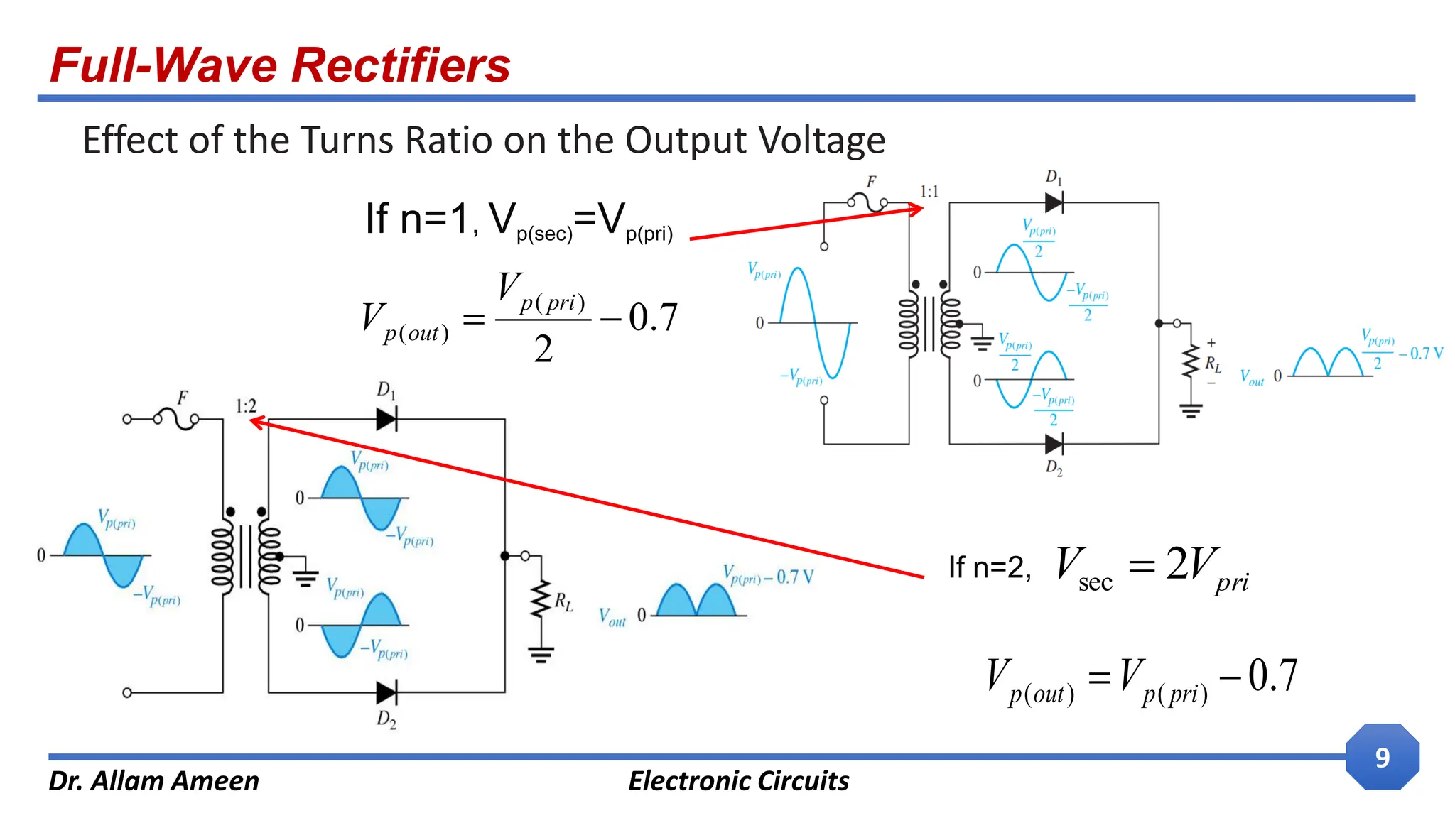
Full-Wave Rectifiers
Dr. AllamAmeen Electronic Circuits
9
Effect of the Turns Ratio on the Output Voltage
If n=1, Vp(sec)=Vp(pri)
If n=2,
7
.
0
)
(
)
(
pri
p
out
p V
V
pri
V
V 2
sec
7
.
0
2
)
(
)
(
pri
p
out
p
V
V
10.
Full-Wave Rectifiers
Dr. AllamAmeen Electronic Circuits
10
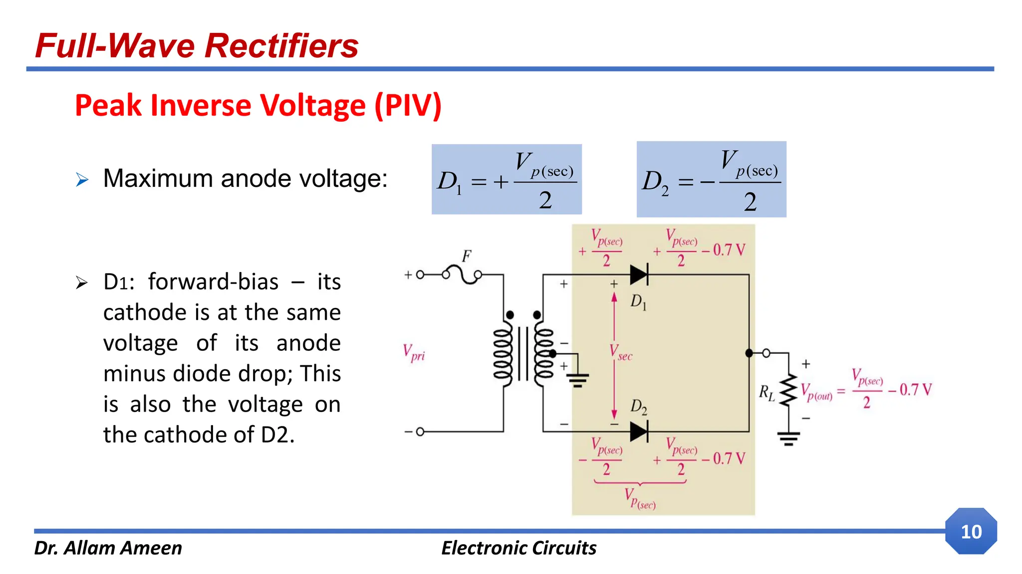
Peak Inverse Voltage (PIV)
Maximum anode voltage:
2
(sec)
1
p
V
D
2
(sec)
2
p
V
D
D1: forward-bias – its
cathode is at the same
voltage of its anode
minus diode drop; This
is also the voltage on
the cathode of D2.
11.
Full-Wave Rectifiers
Dr. AllamAmeen Electronic Circuits
11
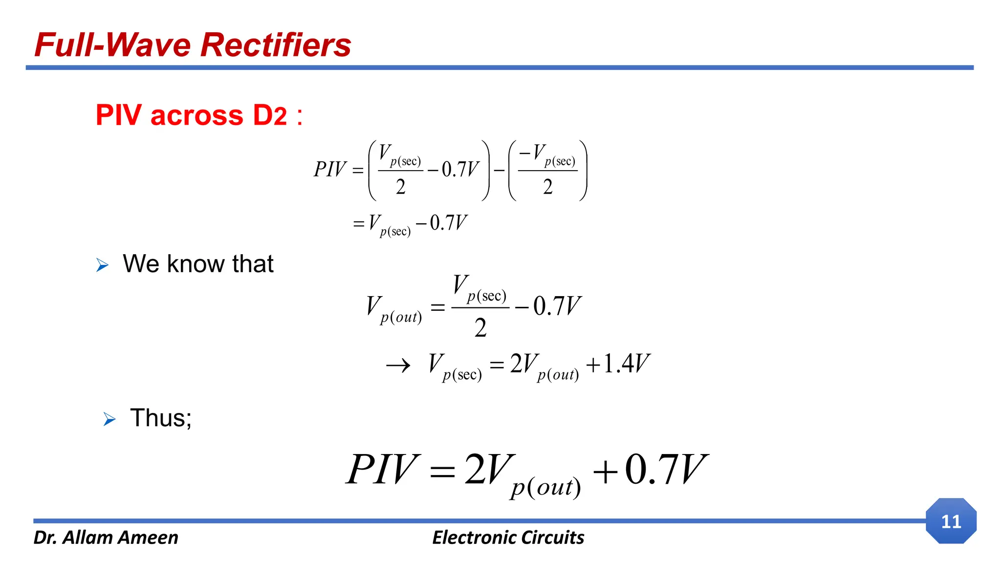
PIV across D2 :
V
V
V
V
V
PIV
p
p
p
7
.
0
2
7
.
0
2
(sec)
(sec)
(sec)
V
V
V
V
V
V
out
p
p
p
out
p
4
.
1
2
7
.
0
2
)
(
(sec)
(sec)
)
(
We know that
Thus;
V
V
PIV out
p 7
.
0
2 )
(
12.
Full-Wave Rectifiers
Dr. AllamAmeen Electronic Circuits
12
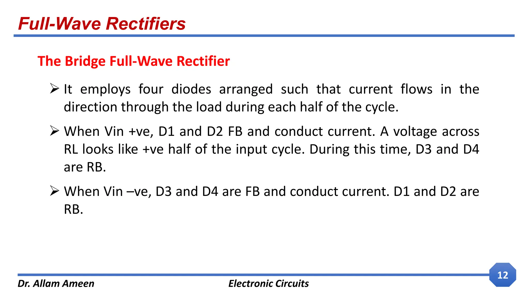
It employs four diodes arranged such that current flows in the
direction through the load during each half of the cycle.
When Vin +ve, D1 and D2 FB and conduct current. A voltage across
RL looks like +ve half of the input cycle. During this time, D3 and D4
are RB.
When Vin –ve, D3 and D4 are FB and conduct current. D1 and D2 are
RB.
The Bridge Full-Wave Rectifier
13.
Full-Wave Rectifiers
Dr. AllamAmeen Electronic Circuits
13
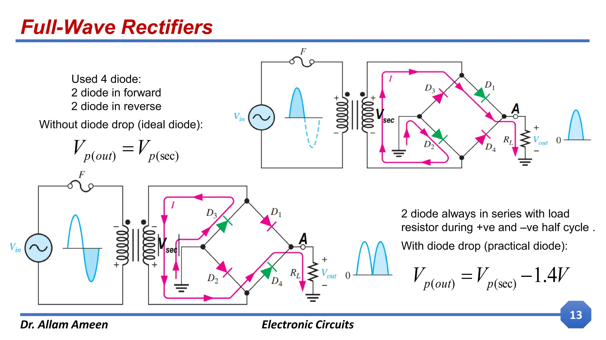
Used 4 diode:
2 diode in forward
2 diode in reverse
Without diode drop (ideal diode):
(sec)
)
( p
out
p V
V
2 diode always in series with load
resistor during +ve and –ve half cycle .
With diode drop (practical diode):
V
V
V p
out
p 4
.
1
(sec)
)
(
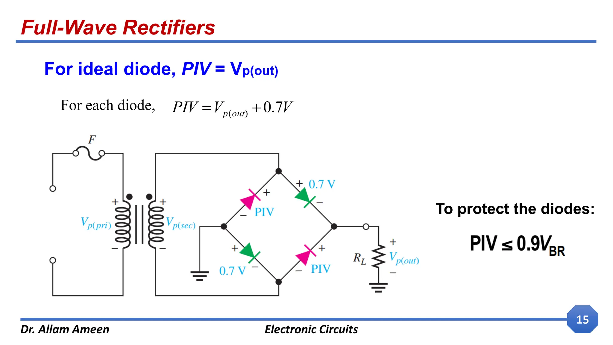
Full-Wave Rectifiers
Dr. AllamAmeen Electronic Circuits
15
For ideal diode, PIV = Vp(out)
V
V
PIV out
p 7
.
0
)
(
For each diode,
To protect the diodes:
16.
Full-Wave Rectifiers
Dr. AllamAmeen Electronic Circuits
16
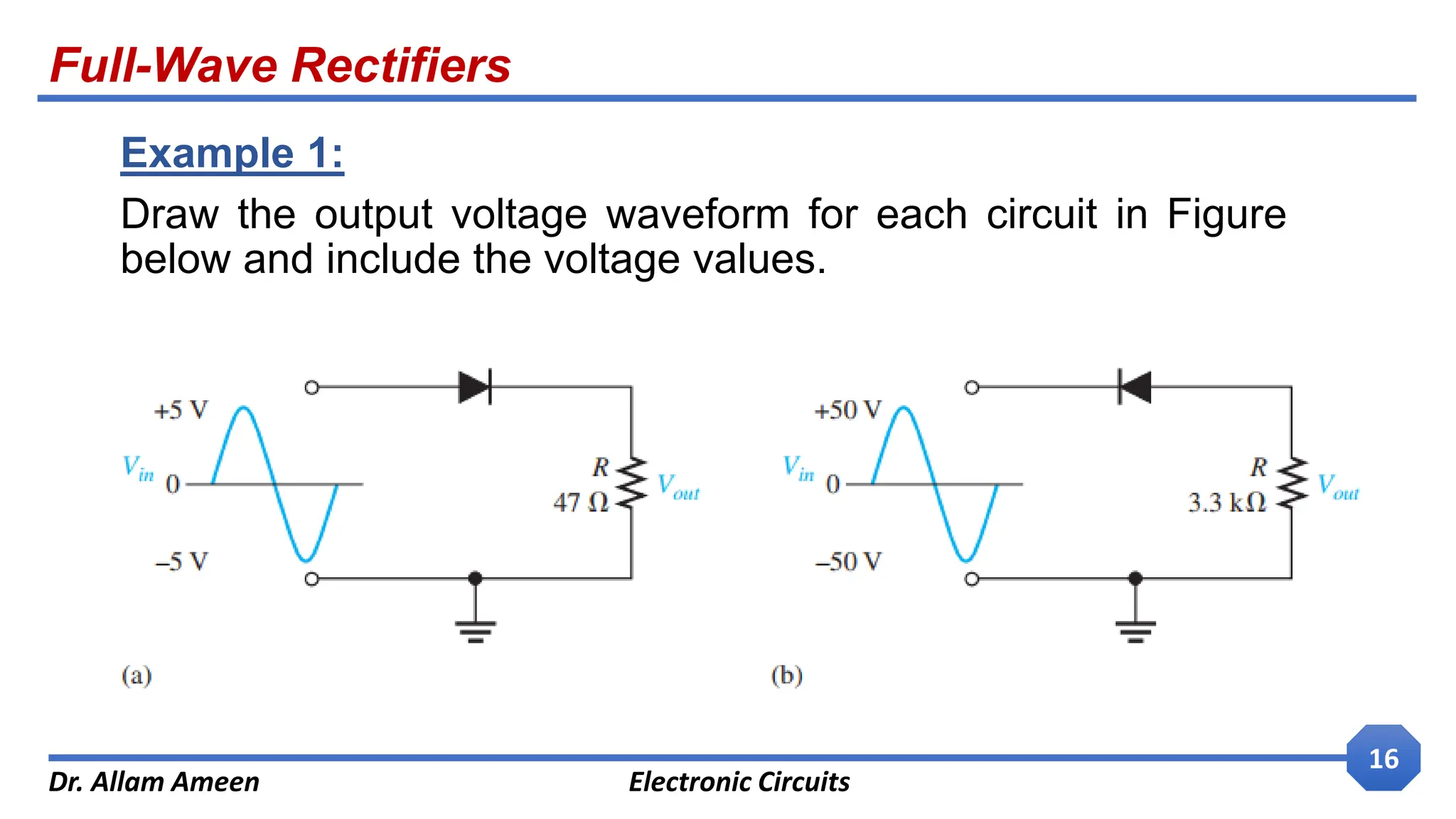
Example 1:
Draw the output voltage waveform for each circuit in Figure
below and include the voltage values.
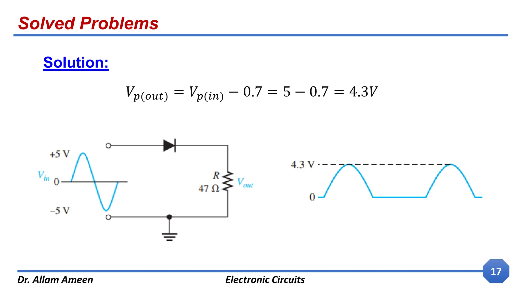
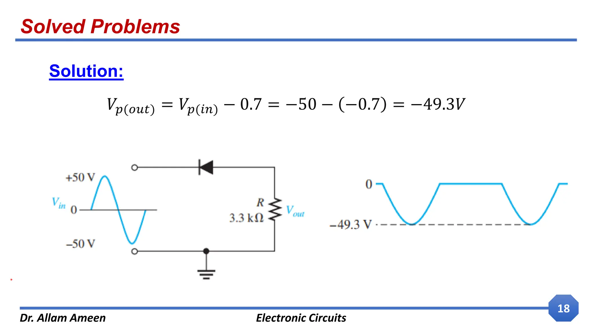
Solved Problems
Dr. AllamAmeen Electronic Circuits
19
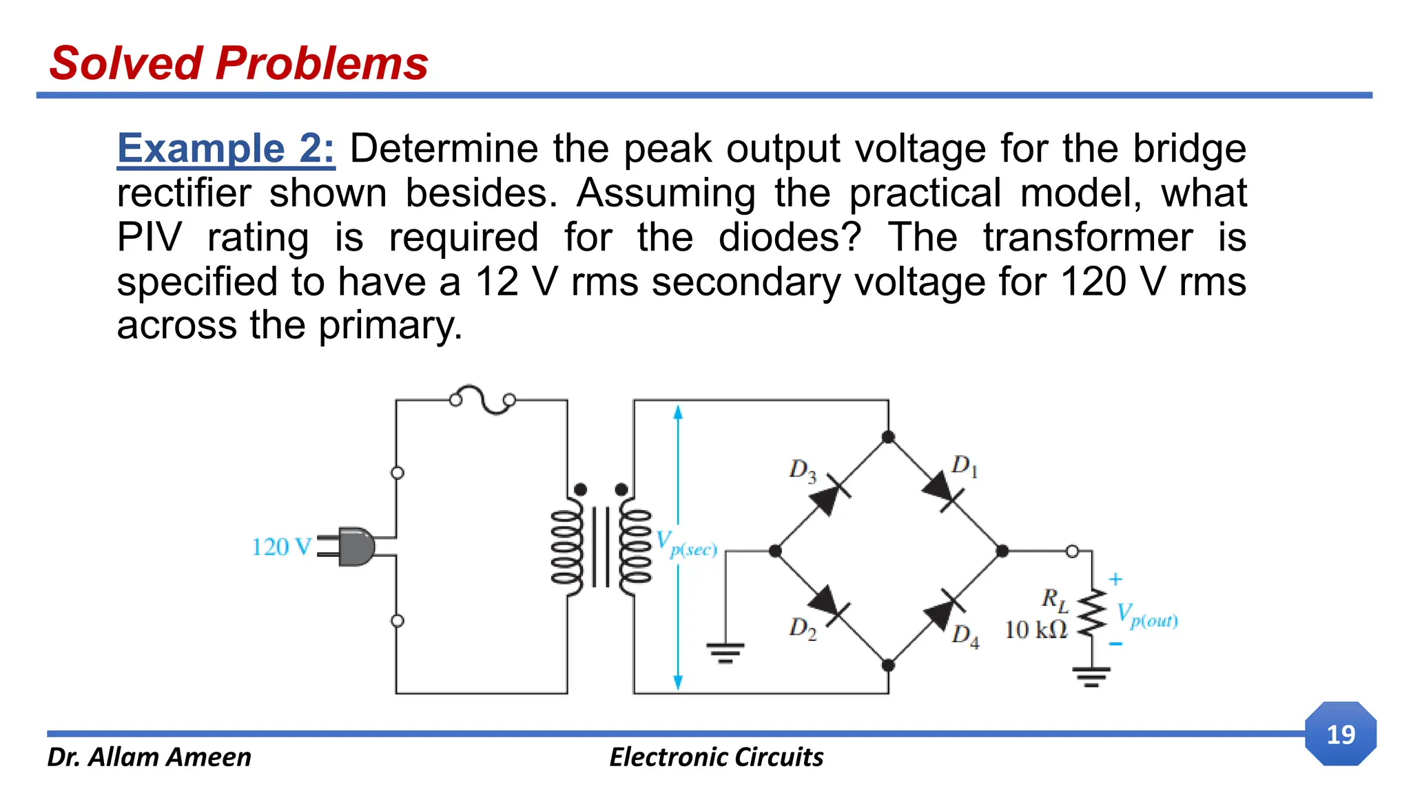
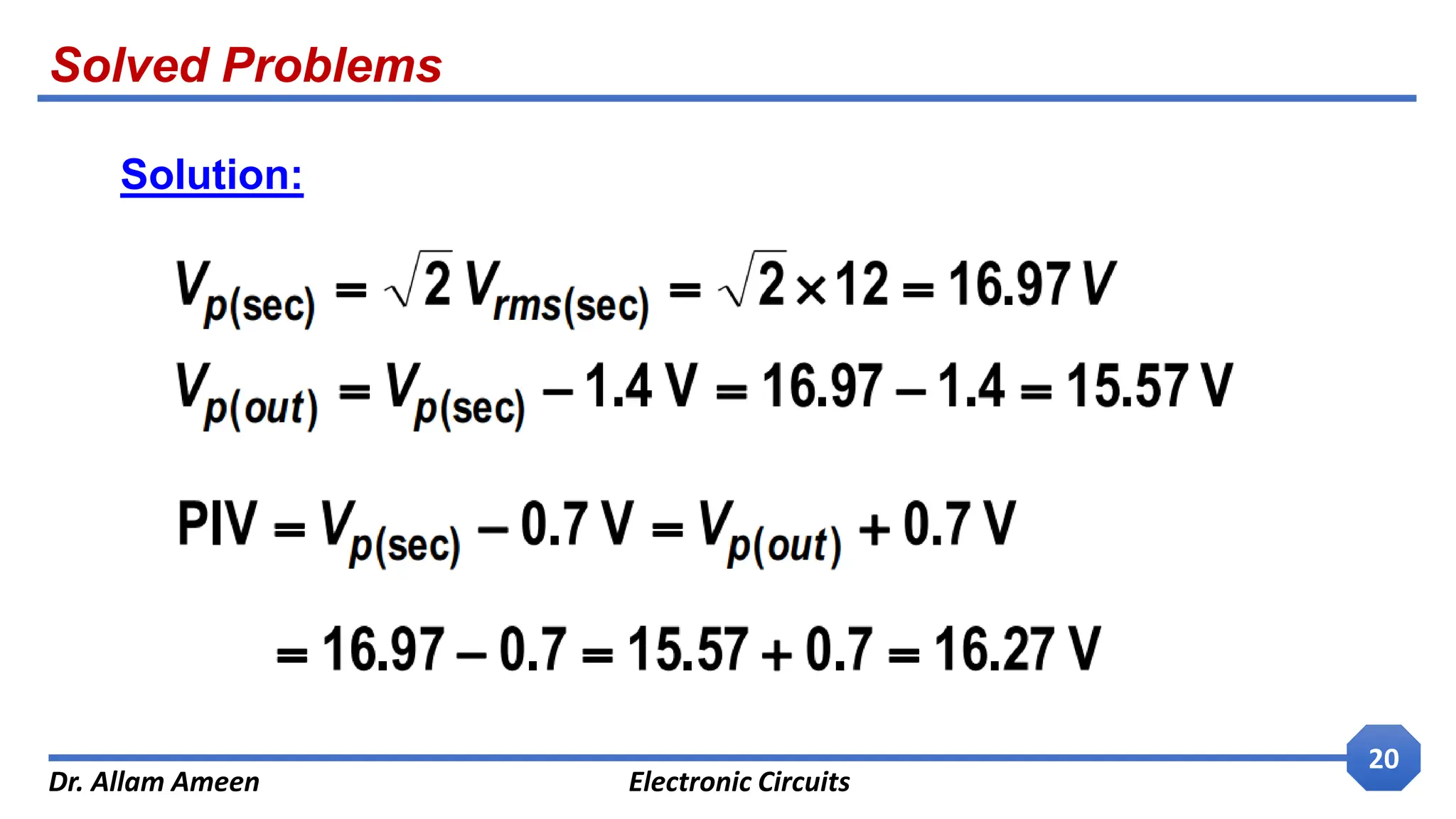
Example 2: Determine the peak output voltage for the bridge
rectifier shown besides. Assuming the practical model, what
PIV rating is required for the diodes? The transformer is
specified to have a 12 V rms secondary voltage for 120 V rms
across the primary.
Power Supply Filters
Dr.Allam Ameen Electronic Circuits
21
To reduce the fluctuations in the output voltage of half / full-
wave rectifier – produces constant-level dc voltage.
It is necessary – electronic circuits require a constant source
to provide power & biasing for proper operation.
Filters are implemented with capacitors.
In most power supply – 50/60 Hz ac power line voltage is
converted to constant dc voltage.
50/60Hz pulsating dc output must be filtered to reduce the
large voltage variation.
22.
Power Supply Filters
Dr.Allam Ameen Electronic Circuits
22
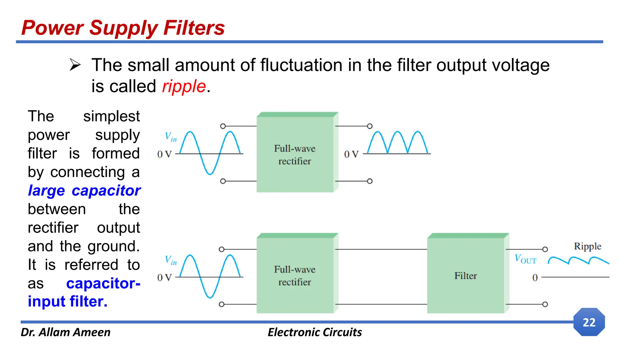
The small amount of fluctuation in the filter output voltage
is called ripple.
The simplest
power supply
filter is formed
by connecting a
large capacitor
between the
rectifier output
and the ground.
It is referred to
as capacitor-
input filter.
23.
Power Supply Filters
Dr.Allam Ameen Electronic Circuits
23
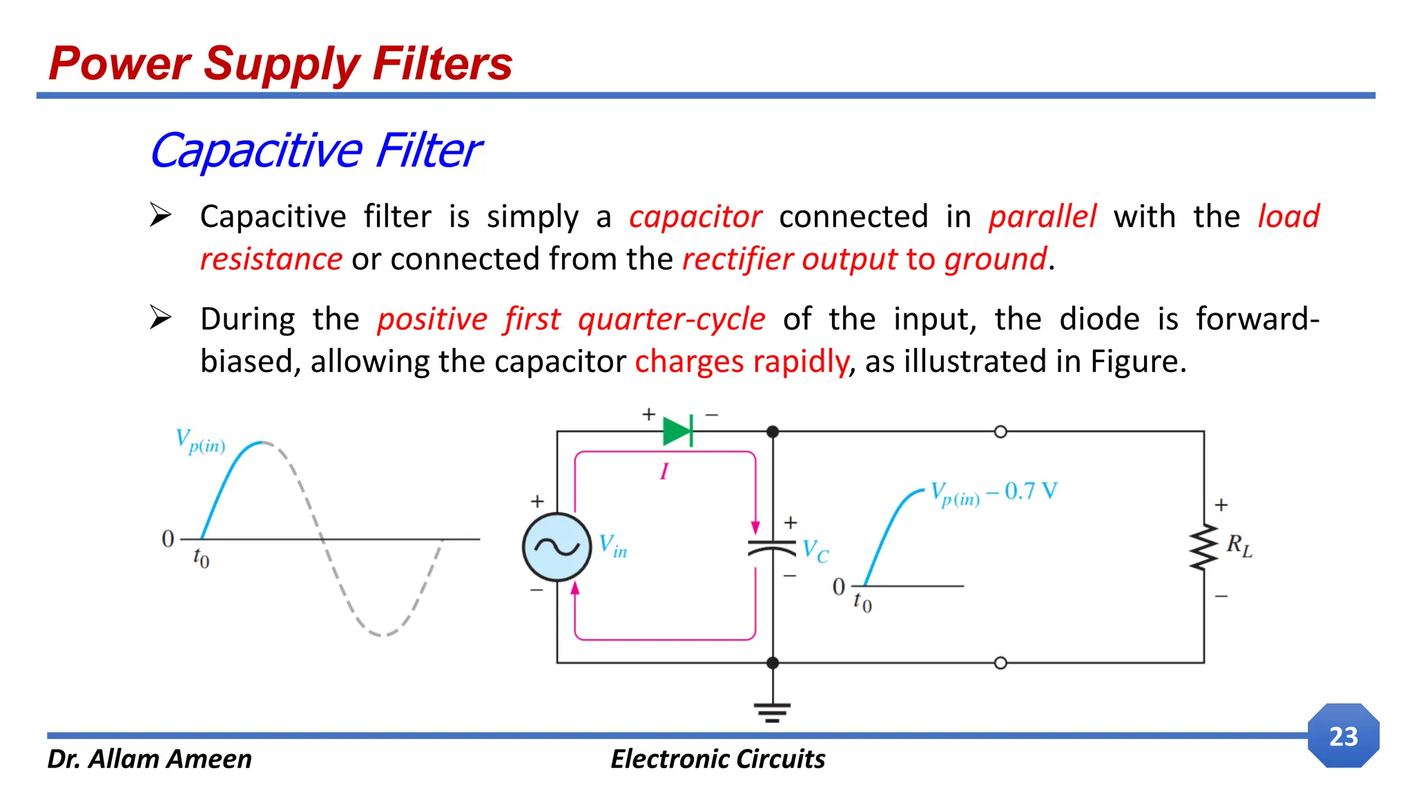
Capacitive Filter
Capacitive filter is simply a capacitor connected in parallel with the load
resistance or connected from the rectifier output to ground.
During the positive first quarter-cycle of the input, the diode is forward-
biased, allowing the capacitor charges rapidly, as illustrated in Figure.
24.
Power Supply Filters
Dr.Allam Ameen Electronic Circuits
24
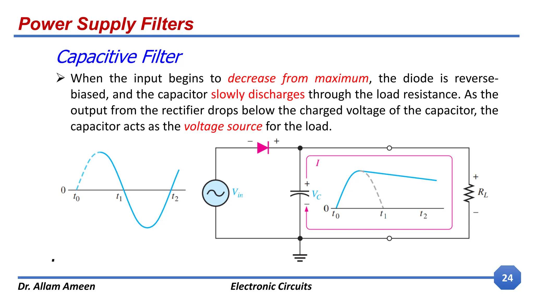
Capacitive Filter
When the input begins to decrease from maximum, the diode is reverse-
biased, and the capacitor slowly discharges through the load resistance. As the
output from the rectifier drops below the charged voltage of the capacitor, the
capacitor acts as the voltage source for the load.
25.
Power Supply Filters
Dr.Allam Ameen Electronic Circuits
25
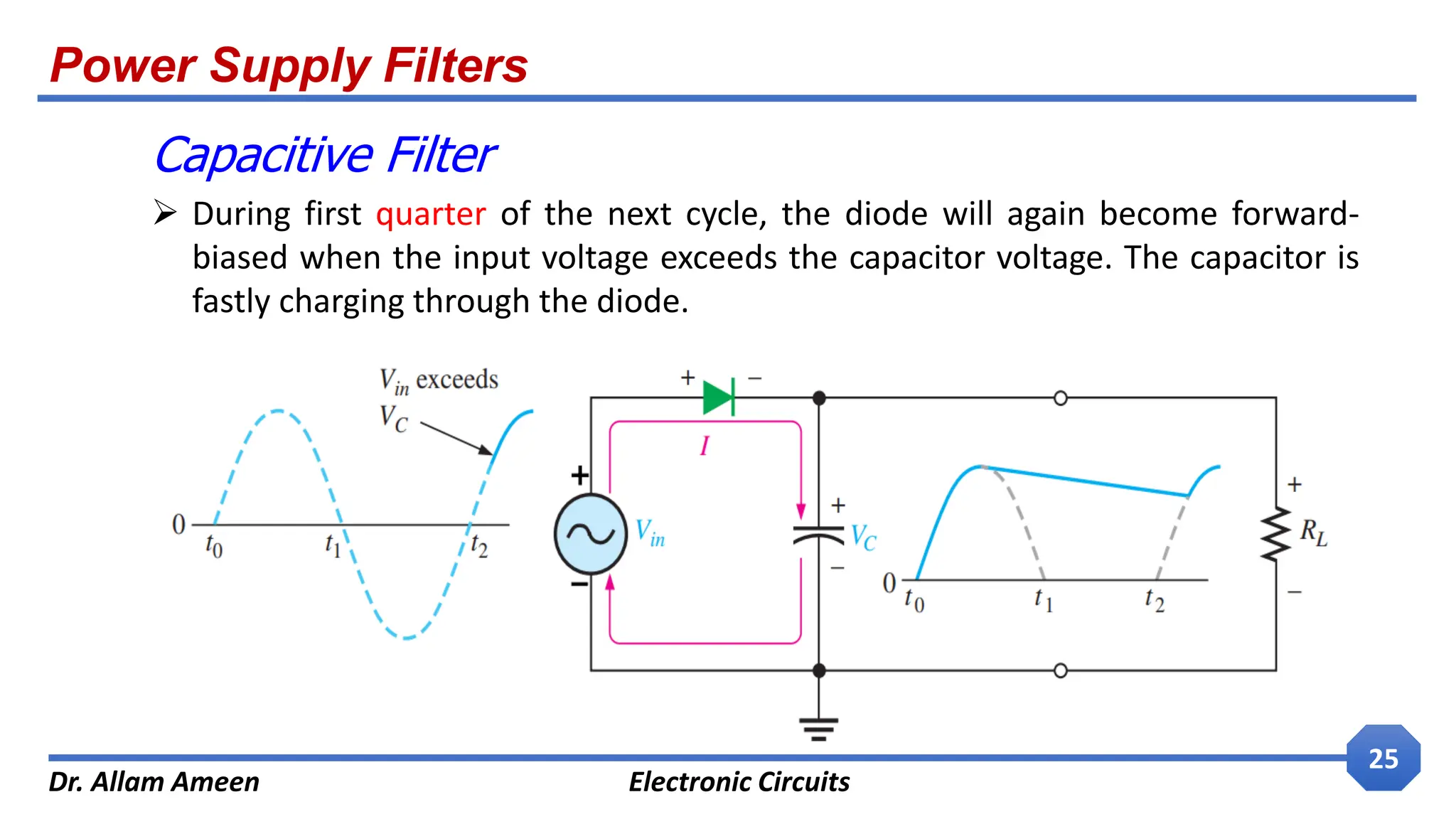
Capacitive Filter
During first quarter of the next cycle, the diode will again become forward-
biased when the input voltage exceeds the capacitor voltage. The capacitor is
fastly charging through the diode.
26.
Power Supply Filters
Dr.Allam Ameen Electronic Circuits
26
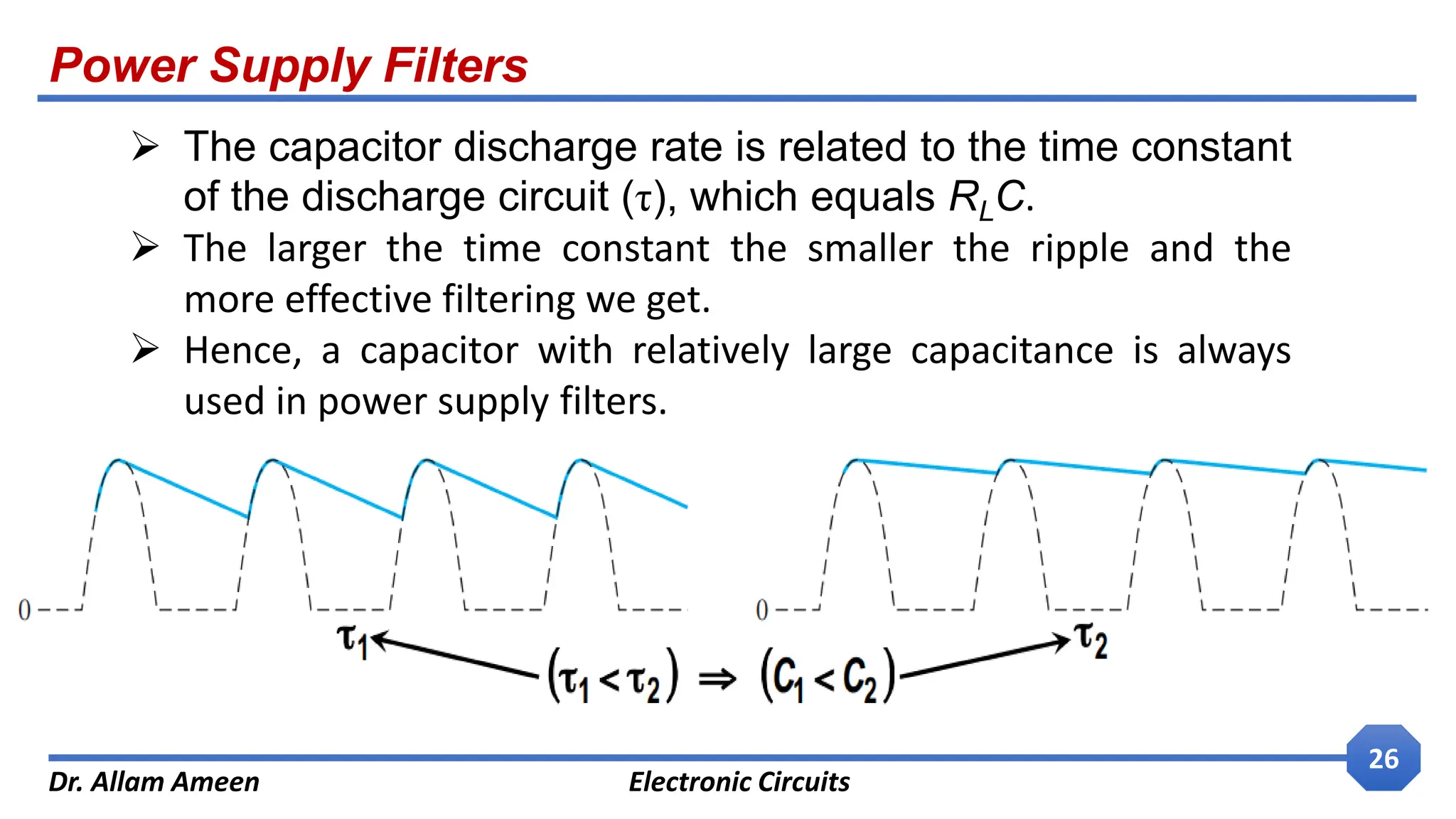
The capacitor discharge rate is related to the time constant
of the discharge circuit (τ), which equals RLC.
The larger the time constant the smaller the ripple and the
more effective filtering we get.
Hence, a capacitor with relatively large capacitance is always
used in power supply filters.
27.
Power Supply Filters
Dr.Allam Ameen Electronic Circuits
27
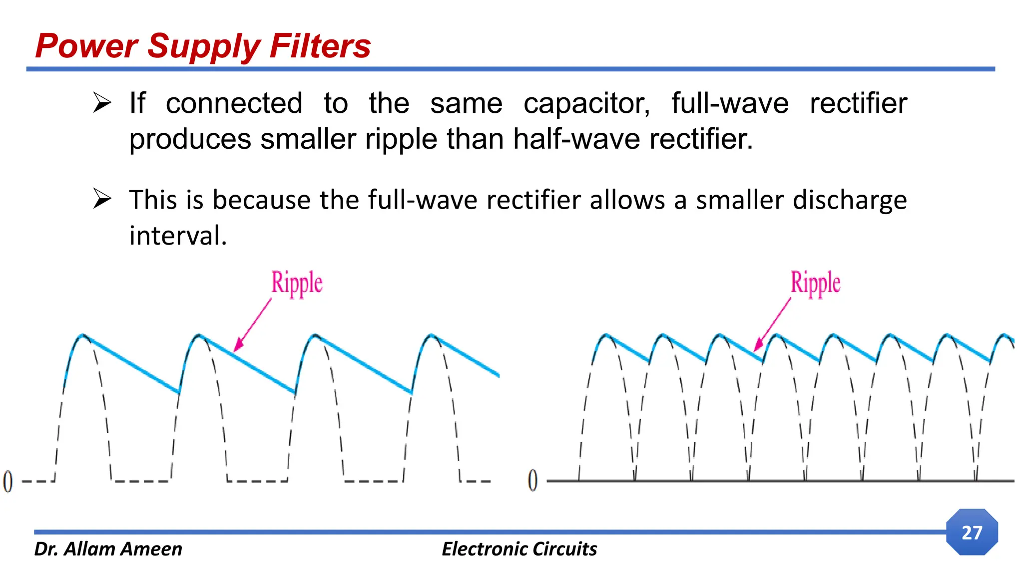
If connected to the same capacitor, full-wave rectifier
produces smaller ripple than half-wave rectifier.
This is because the full-wave rectifier allows a smaller discharge
interval.
28.
Power Supply Filters
Dr.Allam Ameen Electronic Circuits
28
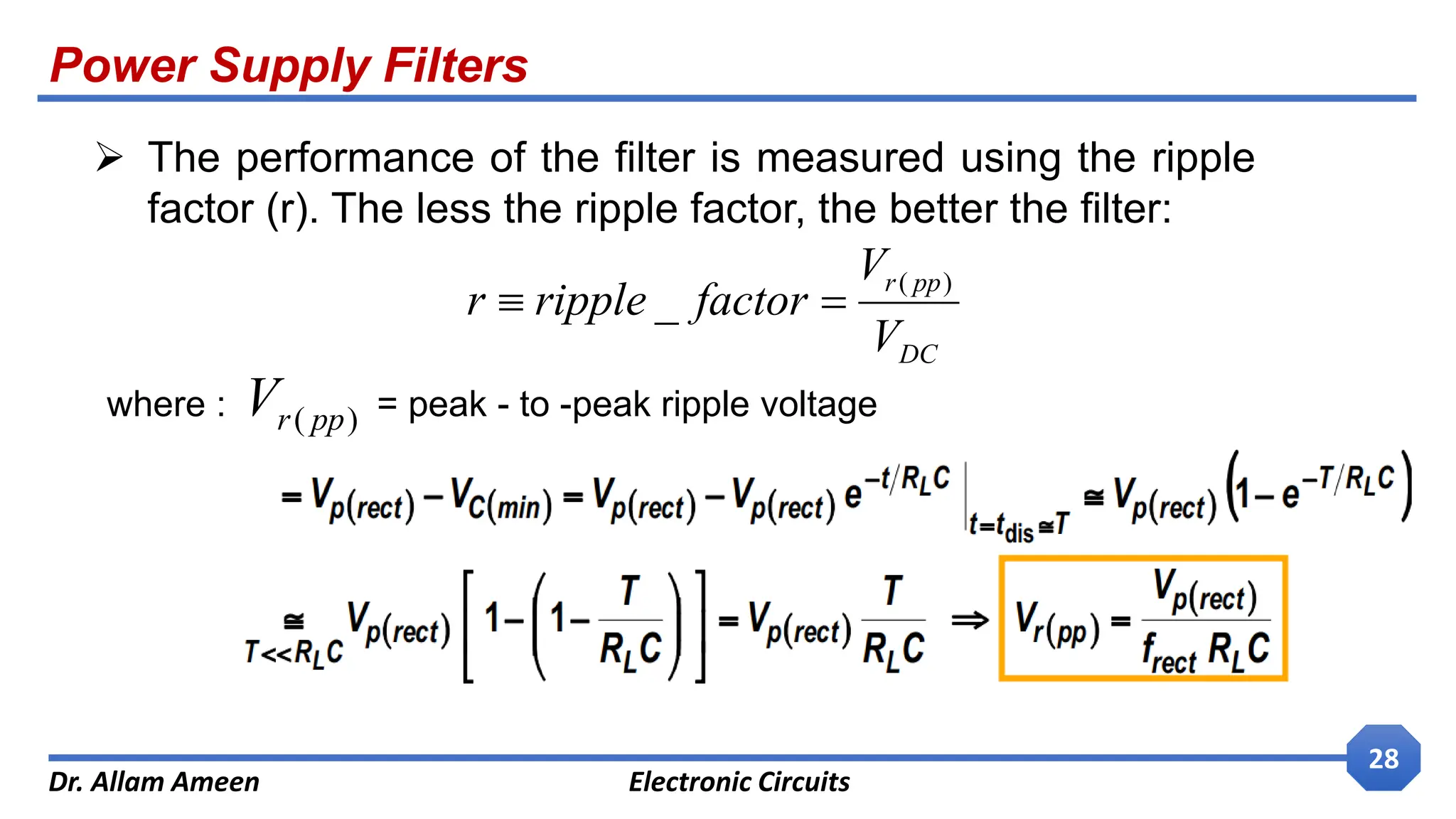
The performance of the filter is measured using the ripple
factor (r). The less the ripple factor, the better the filter:
DC
pp
r
V
V
factor
ripple
r
)
(
_
where : = peak - to -peak ripple voltage
)
( pp
r
V
29.
Power Supply Filters
Dr.Allam Ameen Electronic Circuits
29
Lower ripple factor better filter [can be lowered by
increasing the value of filter capacitor or increasing the load
resistance]
30.
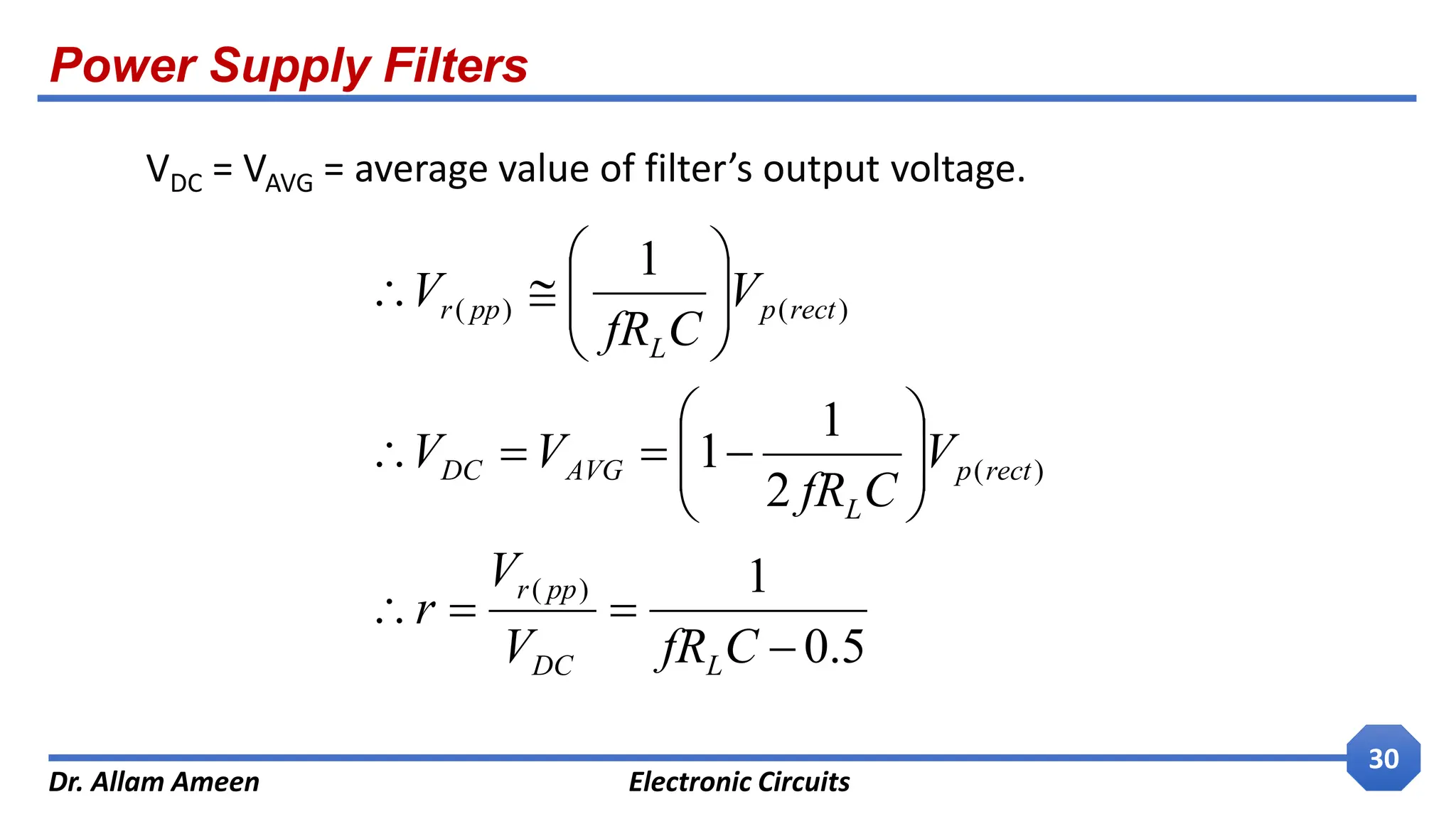
Power Supply Filters
Dr.Allam Ameen Electronic Circuits
30
VDC = VAVG = average value of filter’s output voltage.
5
.
0
1
2
1
1
1
)
(
)
(
)
(
)
(
C
fR
V
V
r
V
C
fR
V
V
V
C
fR
V
L
DC
pp
r
rect
p
L
AVG
DC
rect
p
L
pp
r
31.
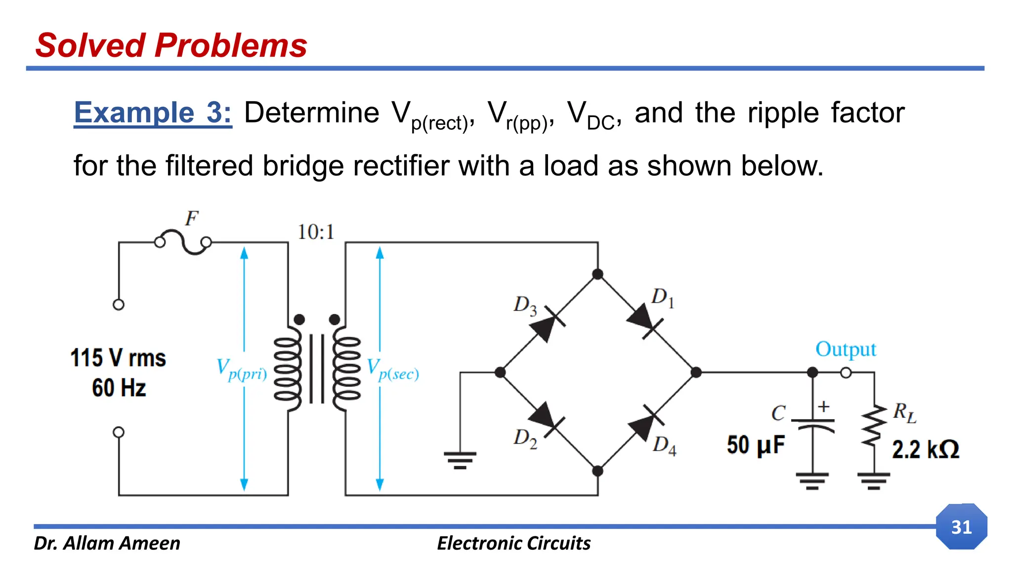
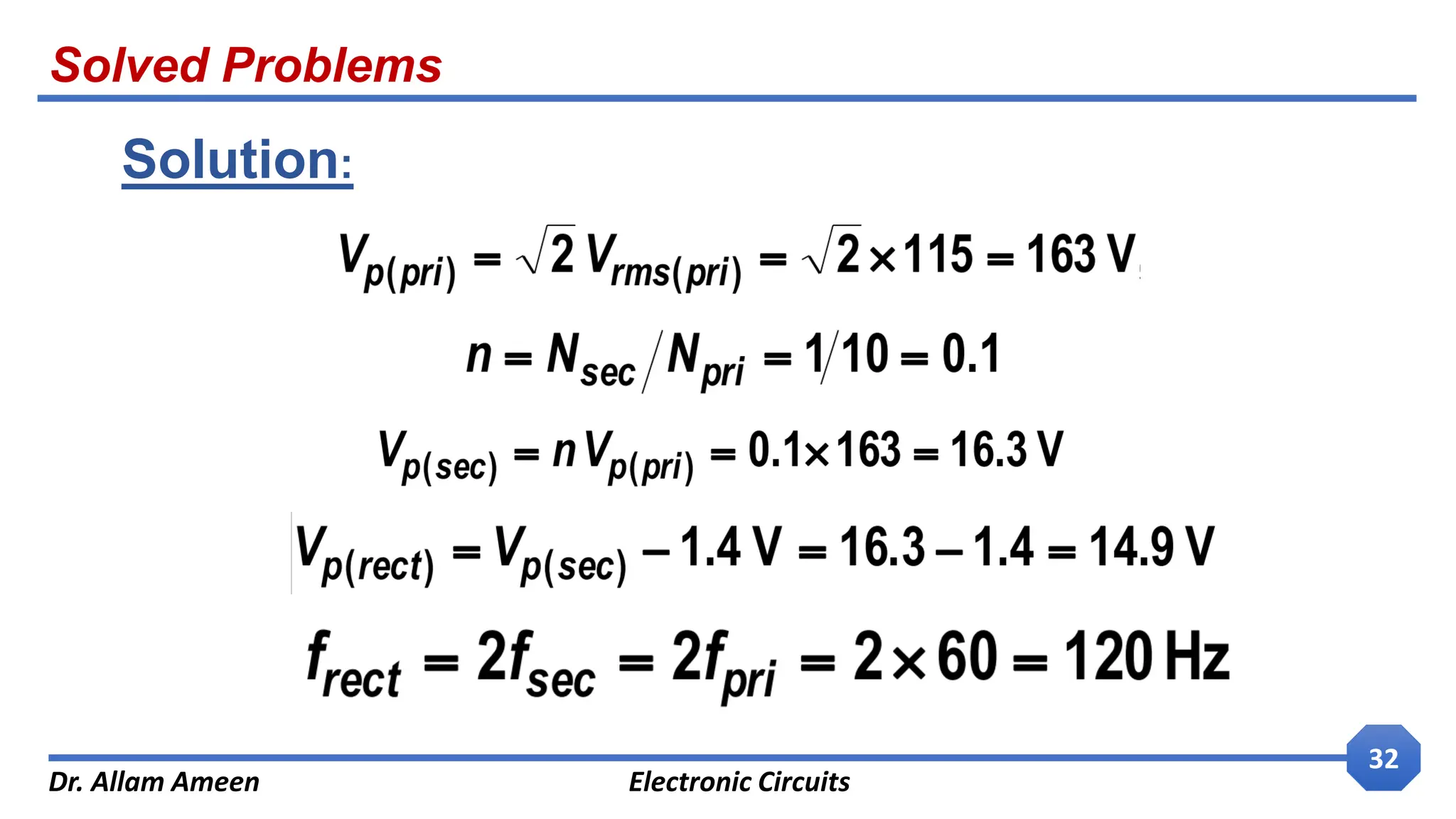
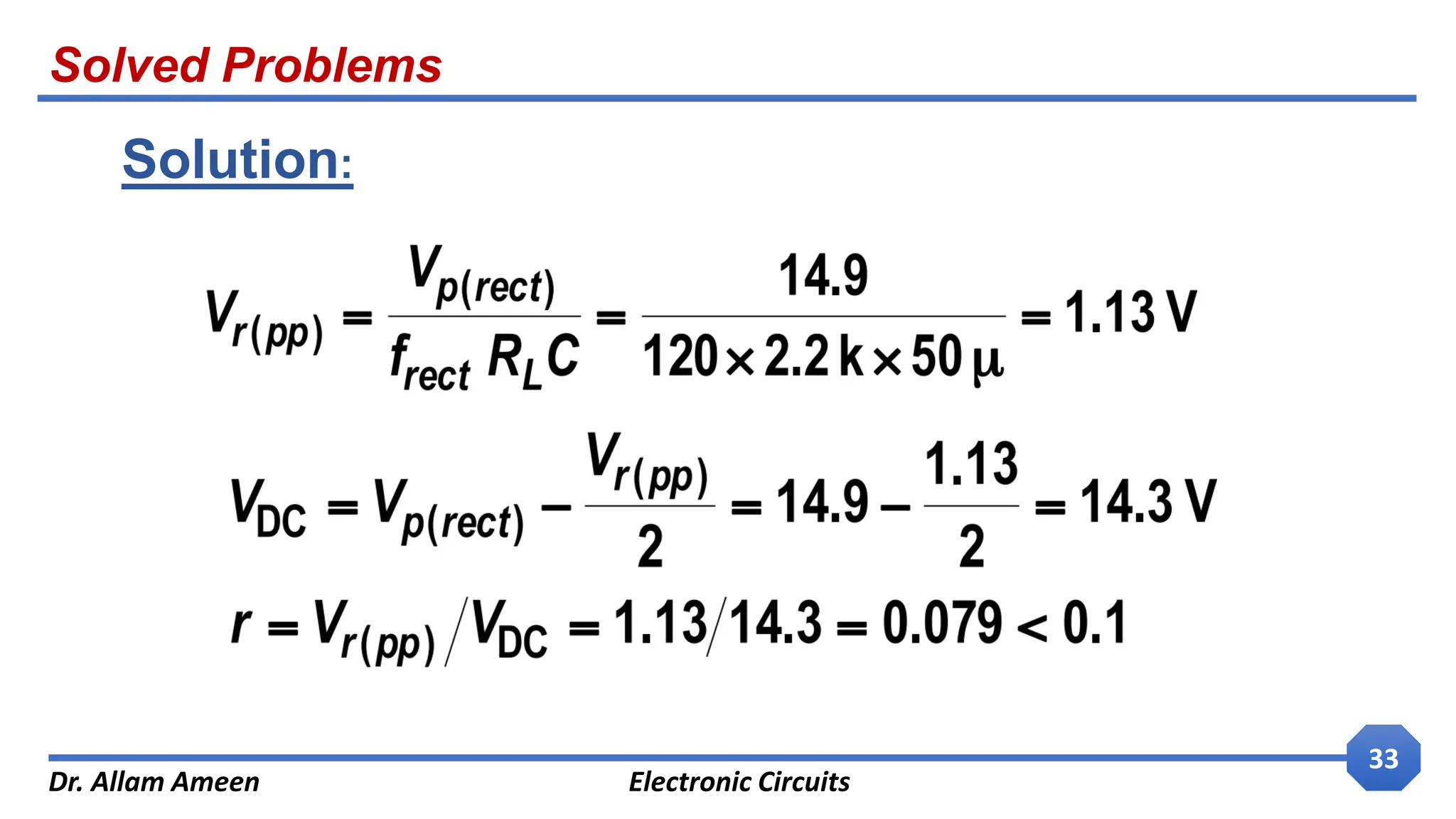
Solved Problems
Dr. AllamAmeen Electronic Circuits
31
Example 3: Determine Vp(rect), Vr(pp), VDC, and the ripple factor
for the filtered bridge rectifier with a load as shown below.
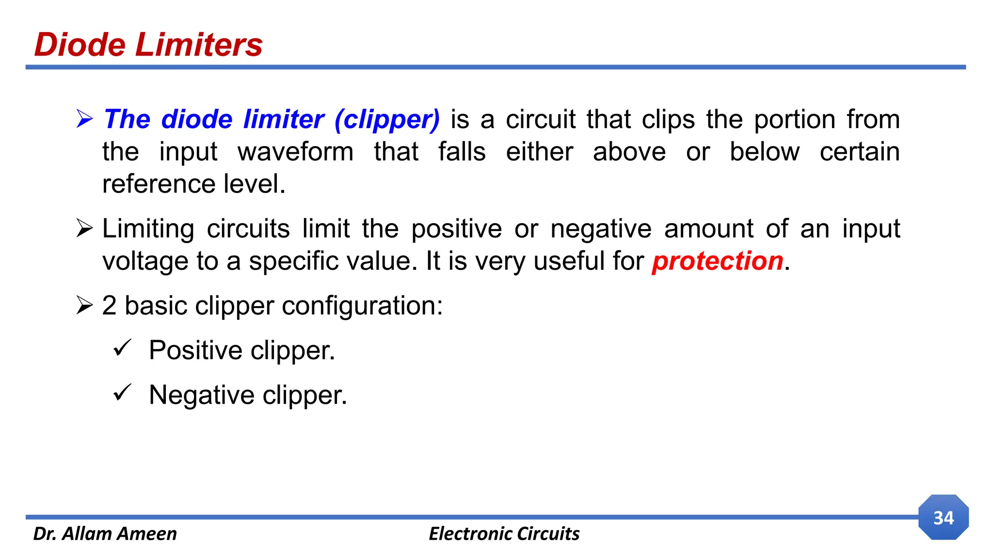
Diode Limiters
Dr. AllamAmeen Electronic Circuits
34
The diode limiter (clipper) is a circuit that clips the portion from
the input waveform that falls either above or below certain
reference level.
Limiting circuits limit the positive or negative amount of an input
voltage to a specific value. It is very useful for protection.
2 basic clipper configuration:
Positive clipper.
Negative clipper.
35.
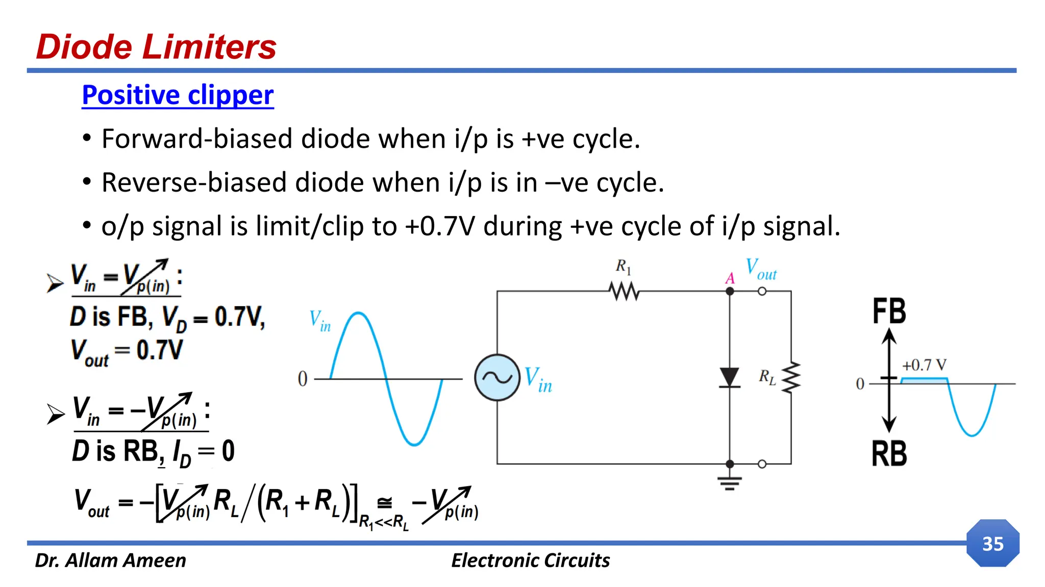
Diode Limiters
Dr. AllamAmeen Electronic Circuits
35
Positive clipper
• Forward-biased diode when i/p is +ve cycle.
• Reverse-biased diode when i/p is in –ve cycle.
• o/p signal is limit/clip to +0.7V during +ve cycle of i/p signal.
36.
Diode Limiters
Dr. AllamAmeen Electronic Circuits
36
Negative clipper
• Reverse-biased diode act as open circuit during +ve cycle.
• Forward-biased diode act as short circuit during –ve cycle.
• o/p signal is limit/clip to -0.7V during –ve cycle of i/p signal.
37.
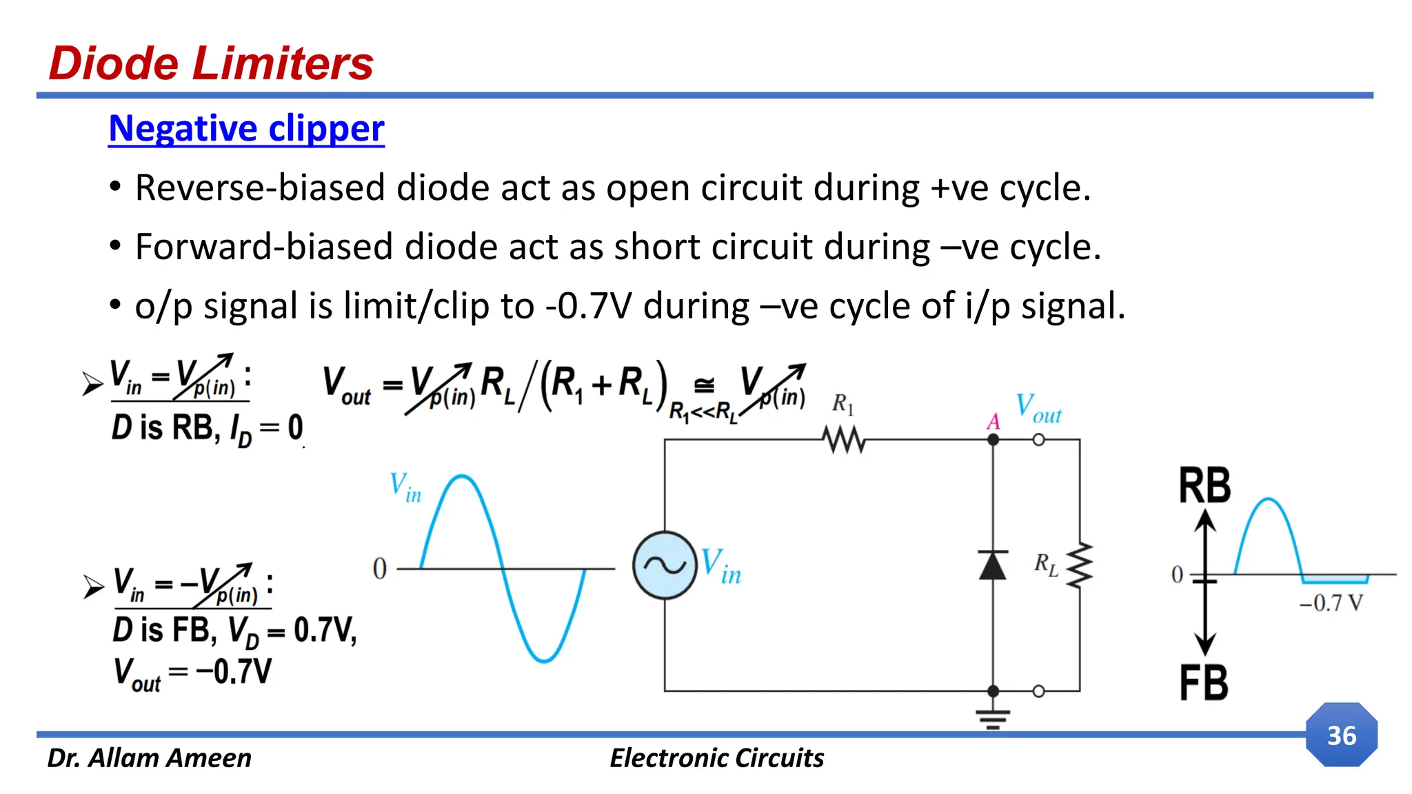
Diode Limiters
Dr. AllamAmeen Electronic Circuits
37
Example 4: What would you expect to see displayed on an
oscilloscope connected across RL in the limiter shown below.
38.
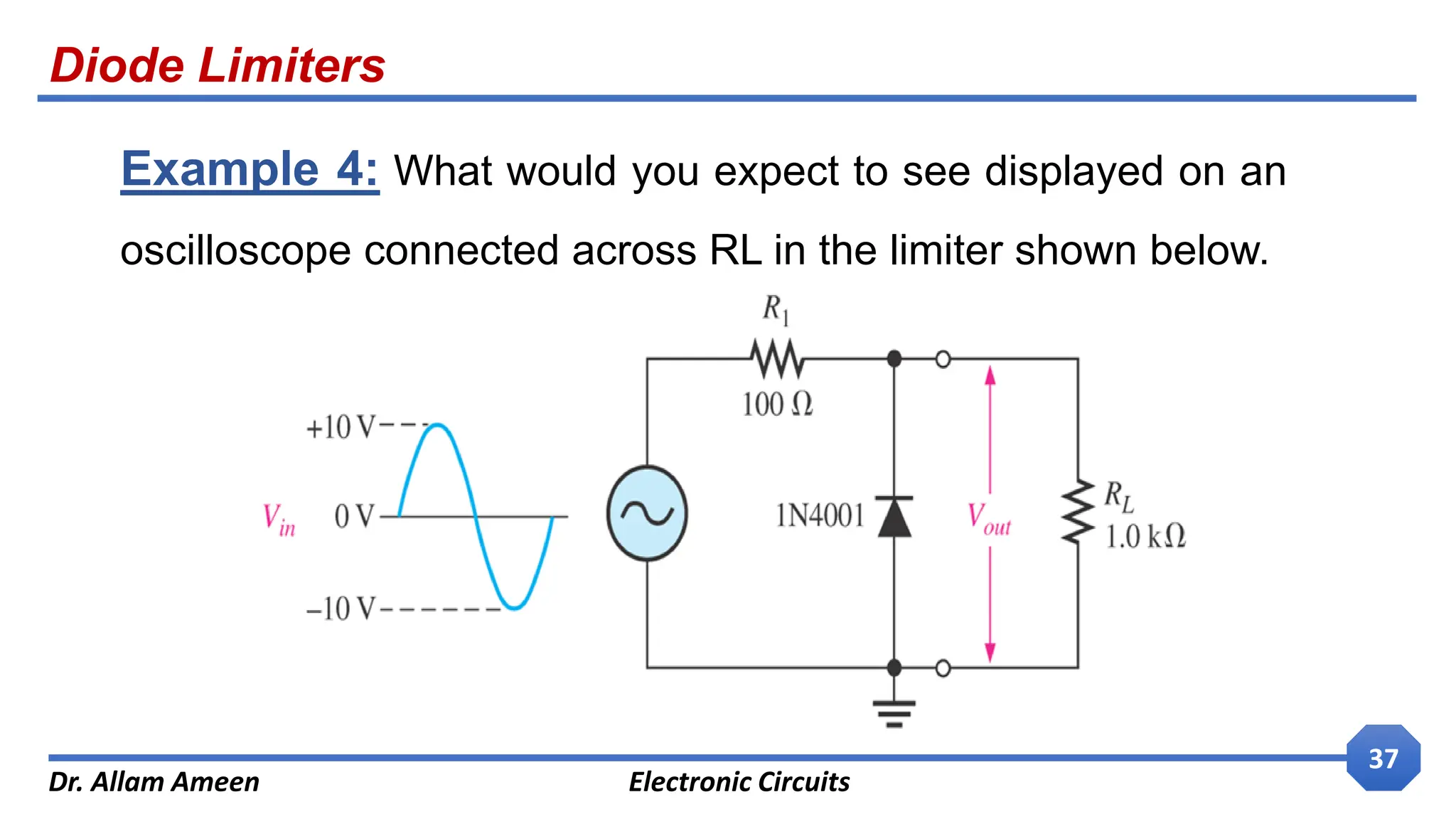
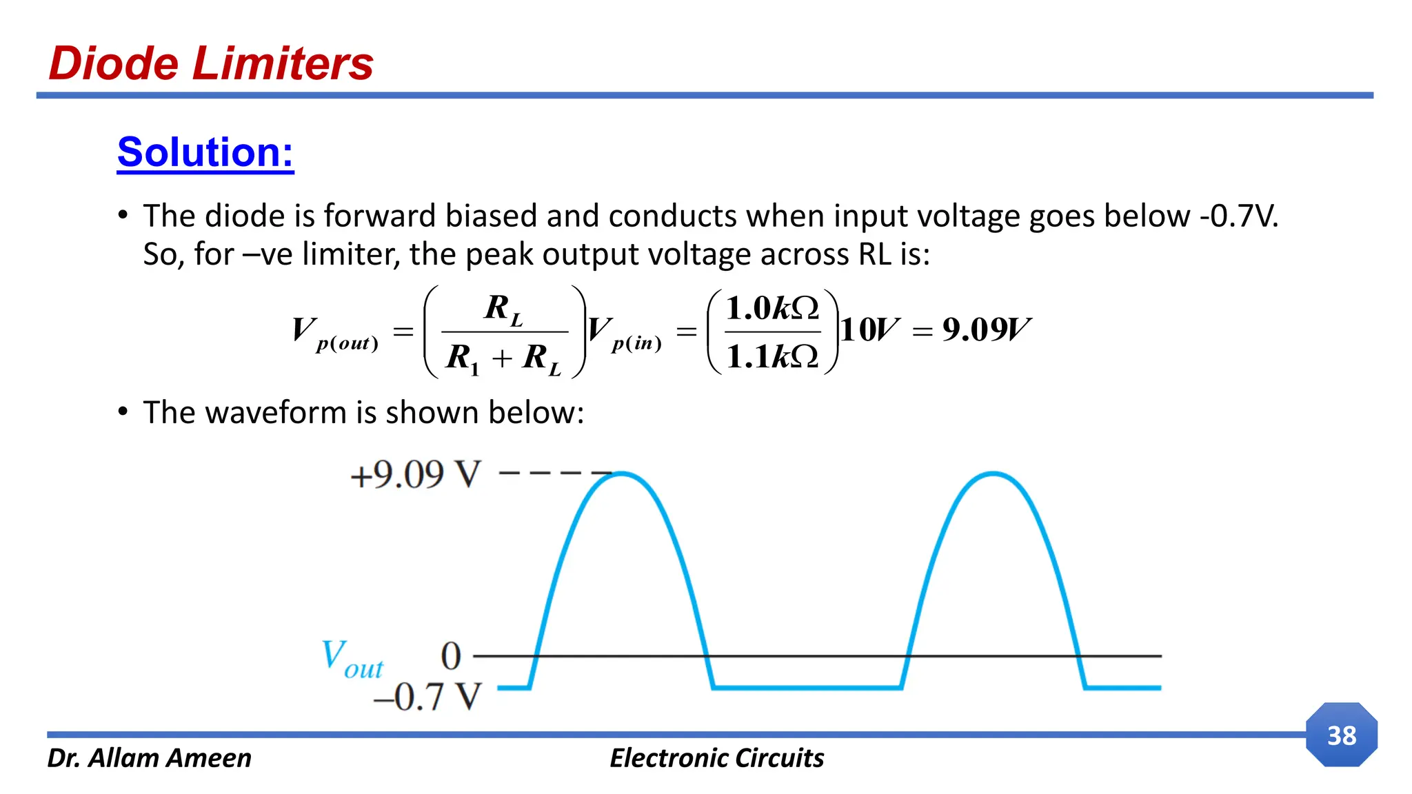
Diode Limiters
Dr. AllamAmeen Electronic Circuits
38
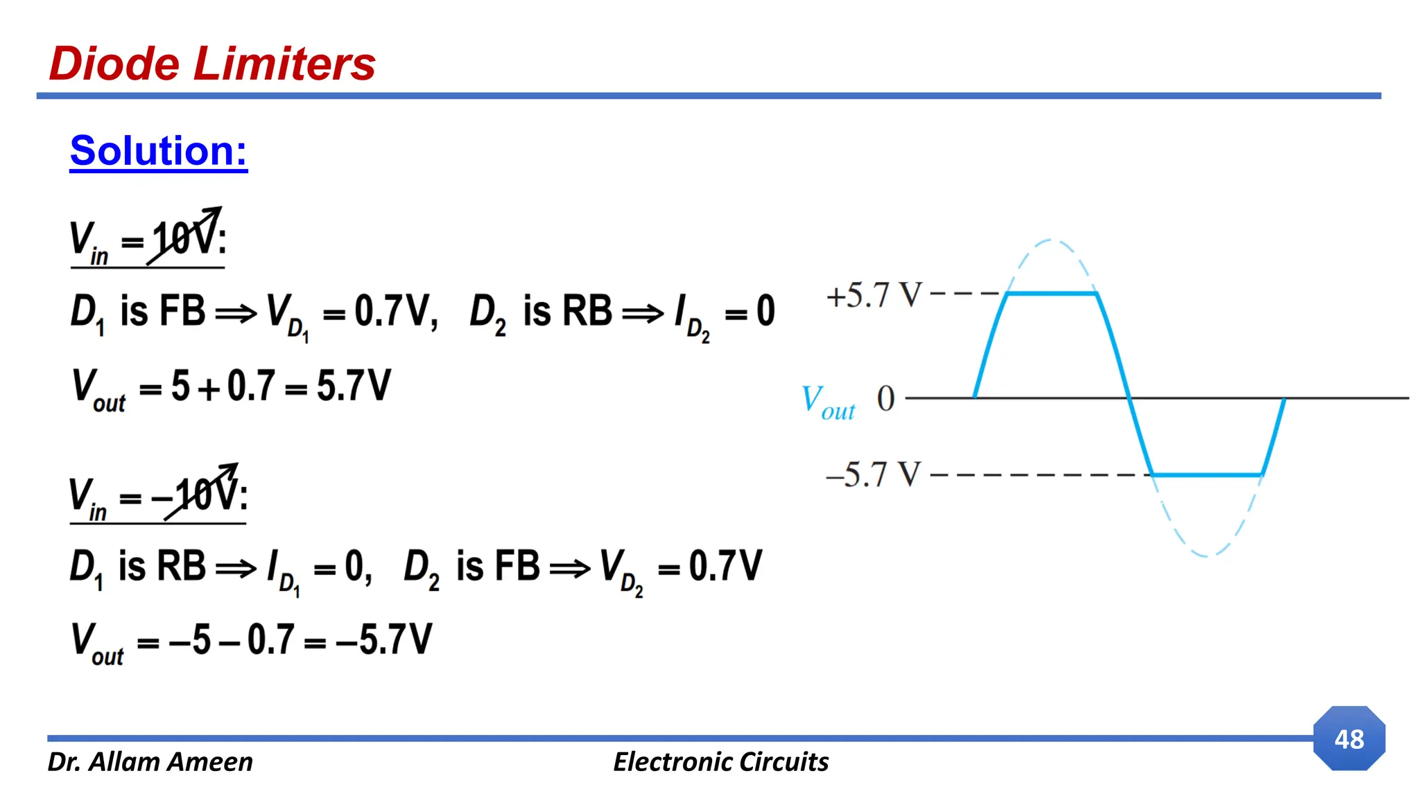
Solution:
• The diode is forward biased and conducts when input voltage goes below -0.7V.
So, for –ve limiter, the peak output voltage across RL is:
• The waveform is shown below:
V
V
k
k
V
R
R
R
V in
p
L
L
out
p 09
.
9
10
1
.
1
0
.
1
)
(
1
)
(
39.
Diode Limiters
Dr. AllamAmeen Electronic Circuits
39
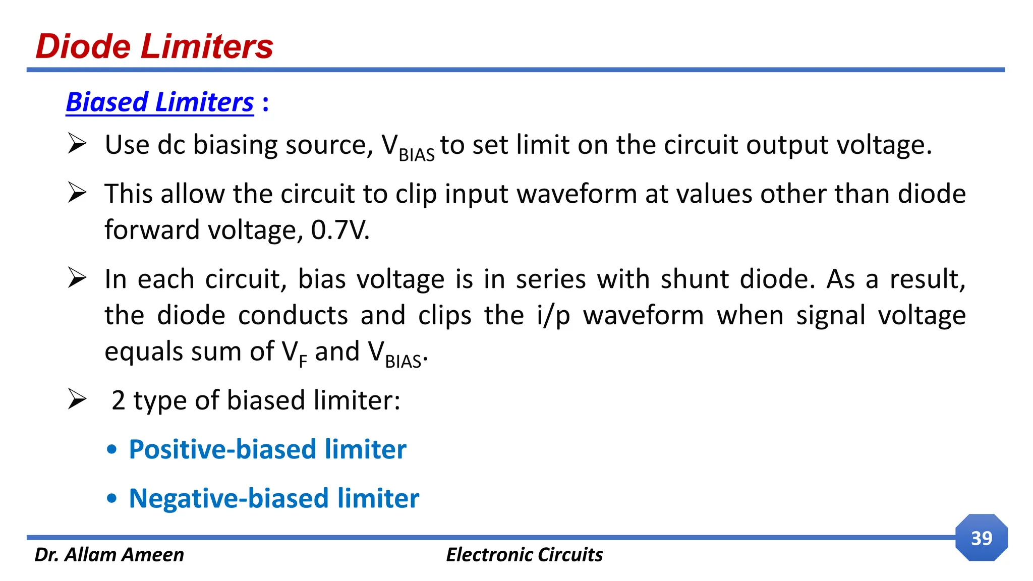
Biased Limiters :
Use dc biasing source, VBIAS to set limit on the circuit output voltage.
This allow the circuit to clip input waveform at values other than diode
forward voltage, 0.7V.
In each circuit, bias voltage is in series with shunt diode. As a result,
the diode conducts and clips the i/p waveform when signal voltage
equals sum of VF and VBIAS.
2 type of biased limiter:
• Positive-biased limiter
• Negative-biased limiter
40.
Diode Limiters
Dr. AllamAmeen Electronic Circuits
40
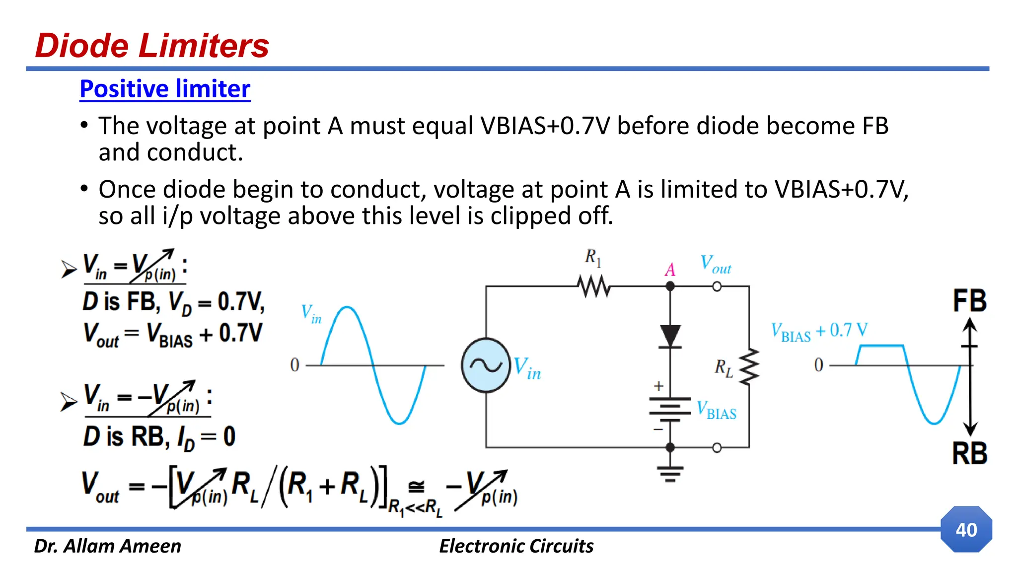
Positive limiter
• The voltage at point A must equal VBIAS+0.7V before diode become FB
and conduct.
• Once diode begin to conduct, voltage at point A is limited to VBIAS+0.7V,
so all i/p voltage above this level is clipped off.
41.
Diode Limiters
Dr. AllamAmeen Electronic Circuits
41
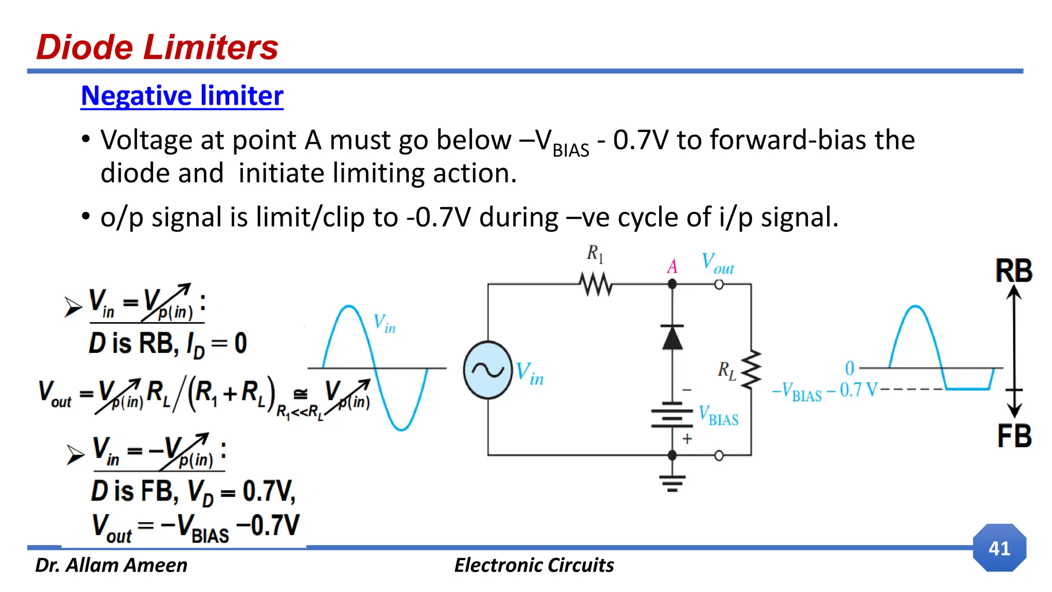
Negative limiter
• Voltage at point A must go below –VBIAS - 0.7V to forward-bias the
diode and initiate limiting action.
• o/p signal is limit/clip to -0.7V during –ve cycle of i/p signal.
42.
Diode Limiters
Dr. AllamAmeen Electronic Circuits
42
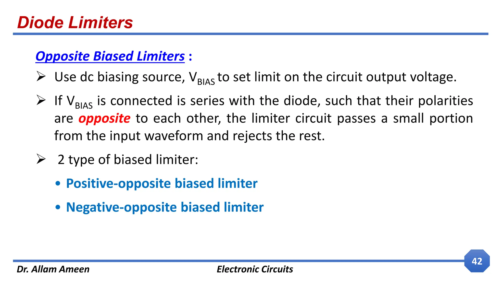
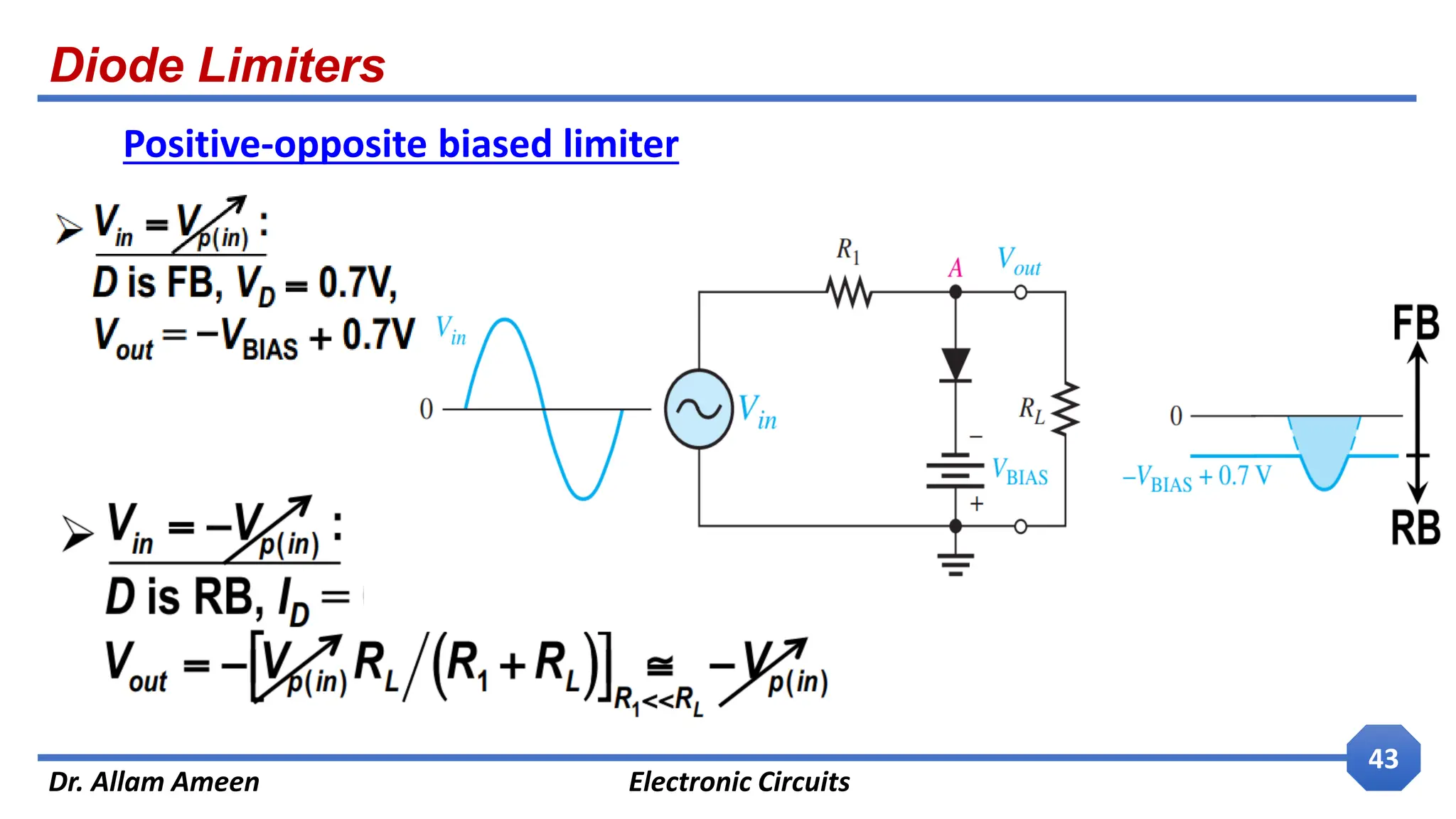
Opposite Biased Limiters :
Use dc biasing source, VBIAS to set limit on the circuit output voltage.
If VBIAS is connected is series with the diode, such that their polarities
are opposite to each other, the limiter circuit passes a small portion
from the input waveform and rejects the rest.
2 type of biased limiter:
• Positive-opposite biased limiter
• Negative-opposite biased limiter
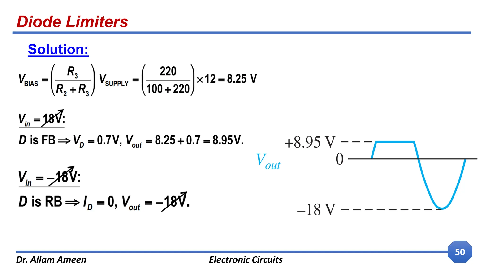
Diode Limiters
Dr. AllamAmeen Electronic Circuits
45
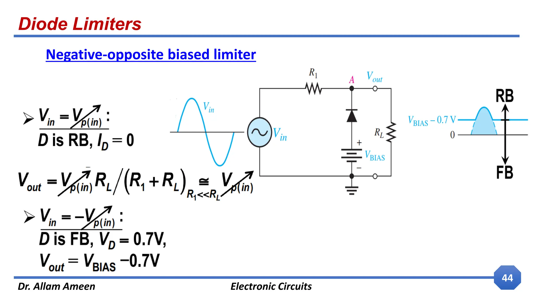
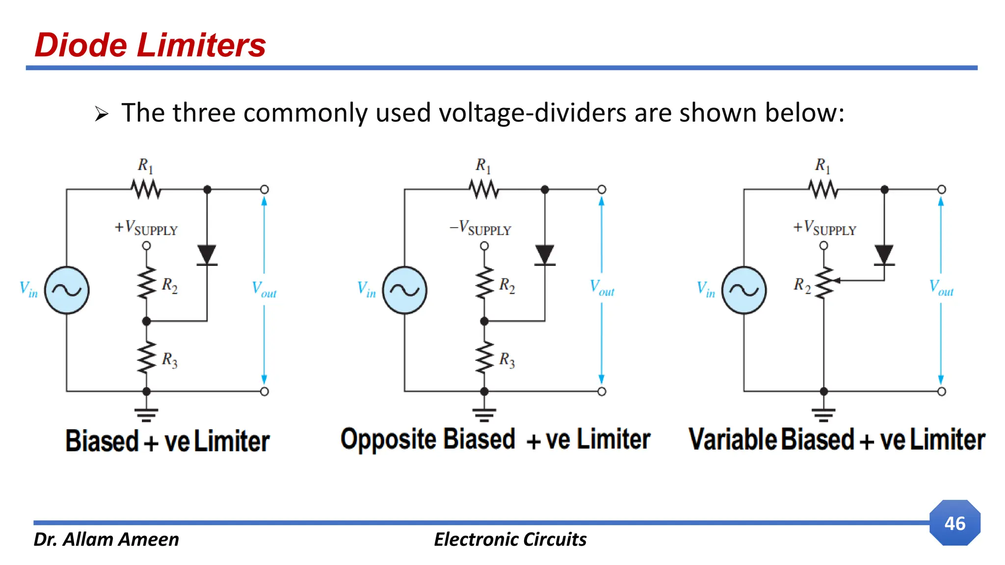
A voltage divider can be used to provide the required bias voltage
(VBIAS) as portion of a supply voltage (VSUPPLY), according to the well-
known voltage-divider formula:
The resistors of the divider (R2 and R3) should be very small
compared to R1 in order to have a stiff voltage divider, and to
minimize the AC voltage drop on (R2 || R3) which may affect VBIAS.
SUPPLY
BIAS V
R
R
R
V
3
2
3
46.
Diode Limiters
Dr. AllamAmeen Electronic Circuits
46
The three commonly used voltage-dividers are shown below:
47.
Diode Limiters
Dr. AllamAmeen Electronic Circuits
47
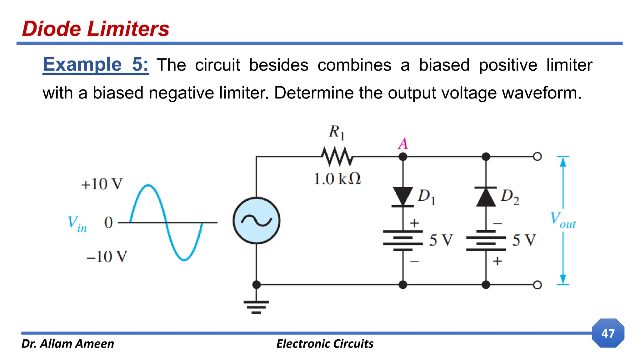
Example 5: The circuit besides combines a biased positive limiter
with a biased negative limiter. Determine the output voltage waveform.
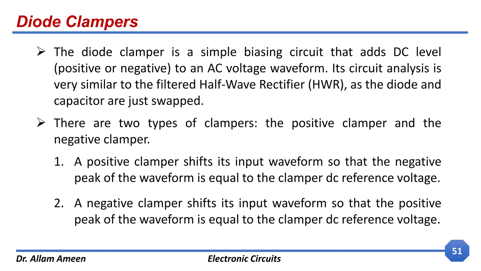
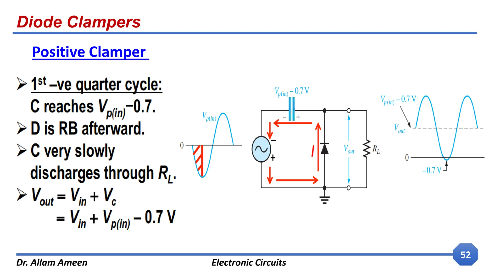
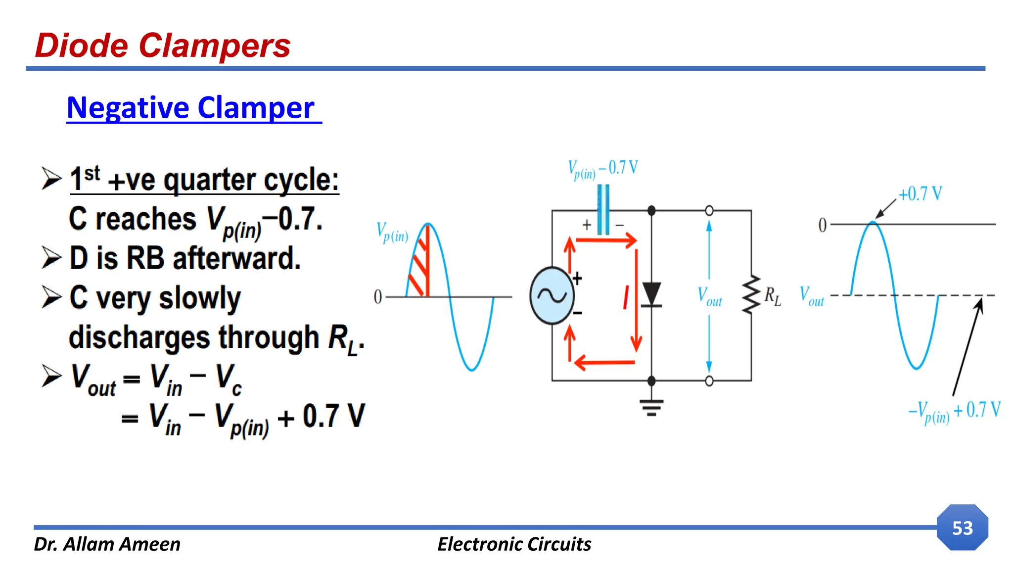
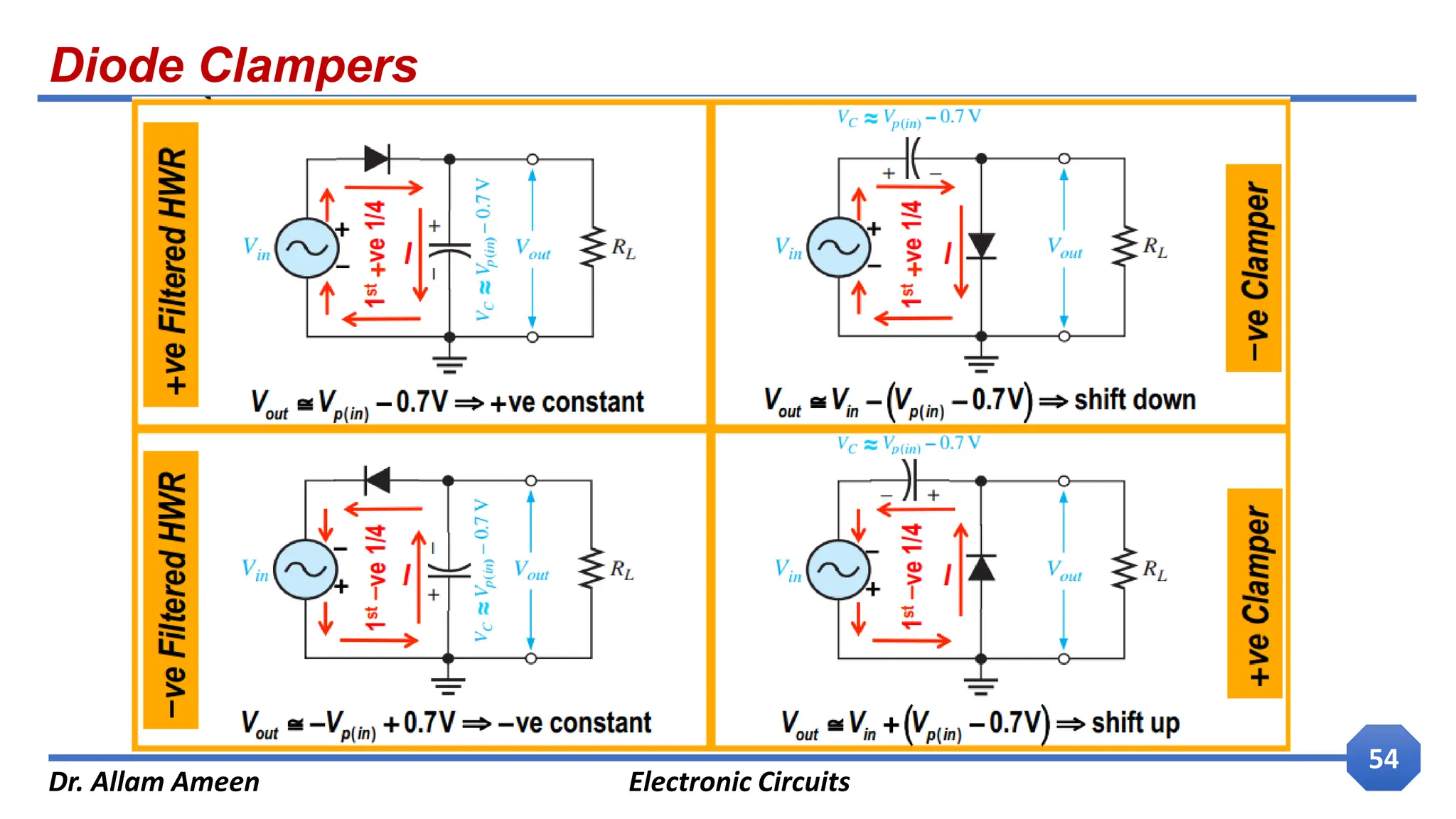
Diode Clampers
Dr. AllamAmeen Electronic Circuits
51
The diode clamper is a simple biasing circuit that adds DC level
(positive or negative) to an AC voltage waveform. Its circuit analysis is
very similar to the filtered Half-Wave Rectifier (HWR), as the diode and
capacitor are just swapped.
There are two types of clampers: the positive clamper and the
negative clamper.
1. A positive clamper shifts its input waveform so that the negative
peak of the waveform is equal to the clamper dc reference voltage.
2. A negative clamper shifts its input waveform so that the positive
peak of the waveform is equal to the clamper dc reference voltage.
Diode Clampers
Dr. AllamAmeen Electronic Circuits
55
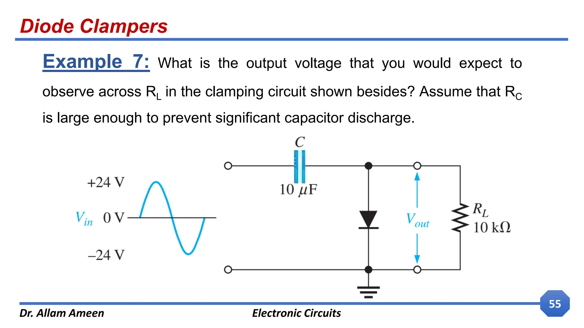
Example 7: What is the output voltage that you would expect to
observe across RL in the clamping circuit shown besides? Assume that RC
is large enough to prevent significant capacitor discharge.
56.
Diode Clampers
Dr. AllamAmeen Electronic Circuits
56
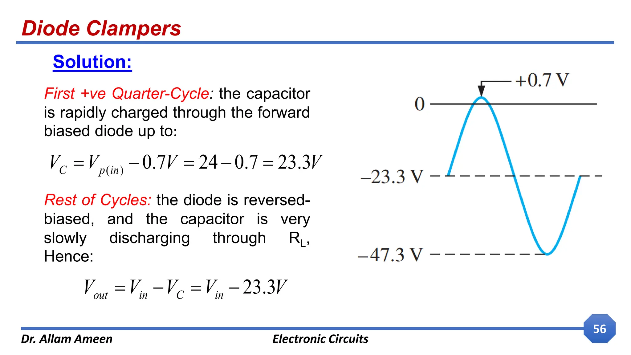
Solution:
First +ve Quarter-Cycle: the capacitor
is rapidly charged through the forward
biased diode up to:
Rest of Cycles: the diode is reversed-
biased, and the capacitor is very
slowly discharging through RL,
Hence:
V
V
V
V in
p
C 3
.
23
7
.
0
24
7
.
0
)
(
V
V
V
V
V in
C
in
out 3
.
23
57.
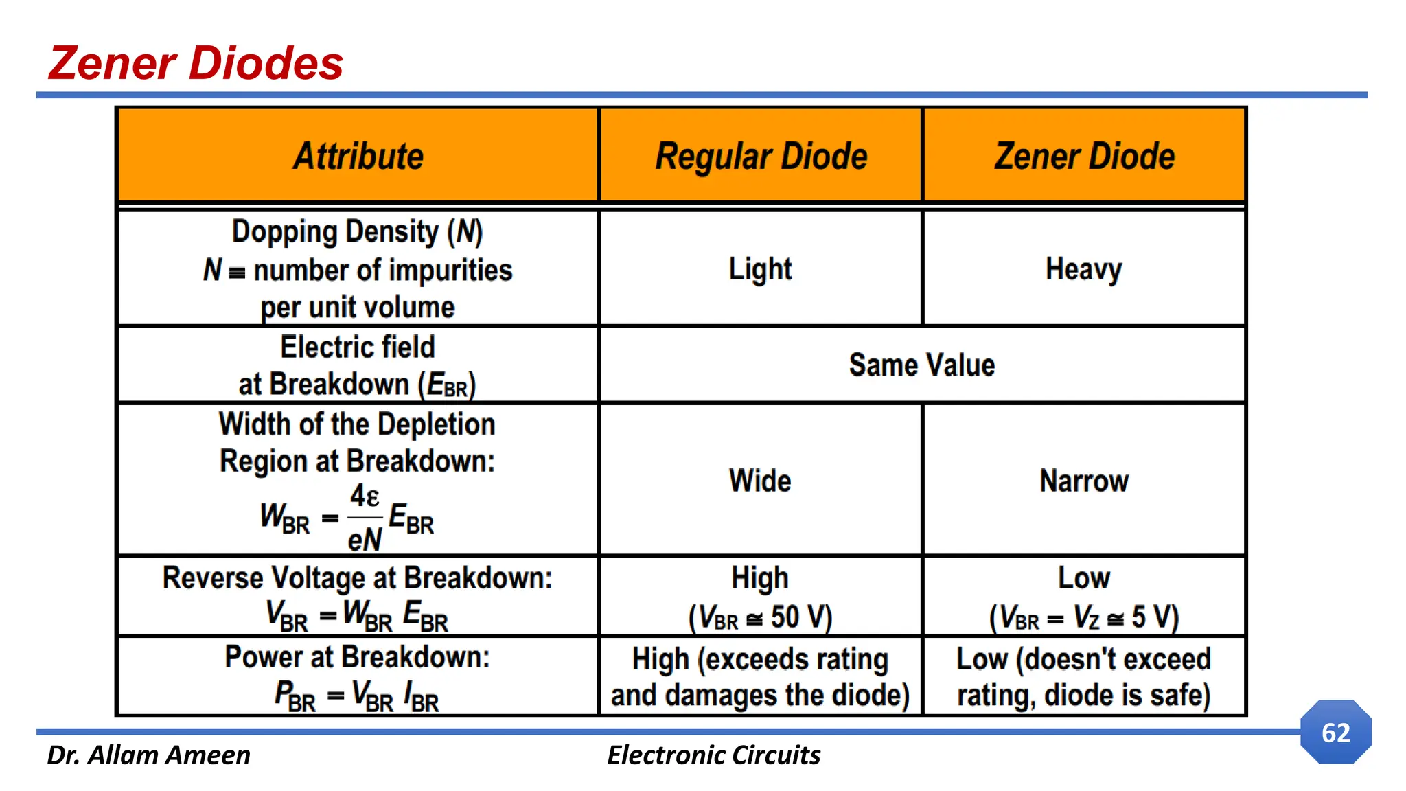
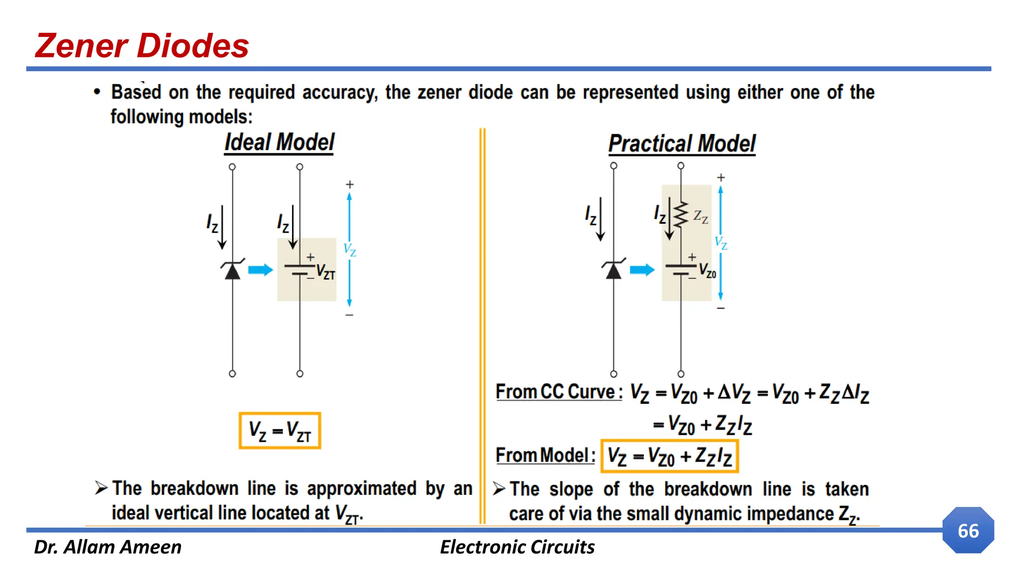
Zener Diodes
Dr. AllamAmeen Electronic Circuits
57
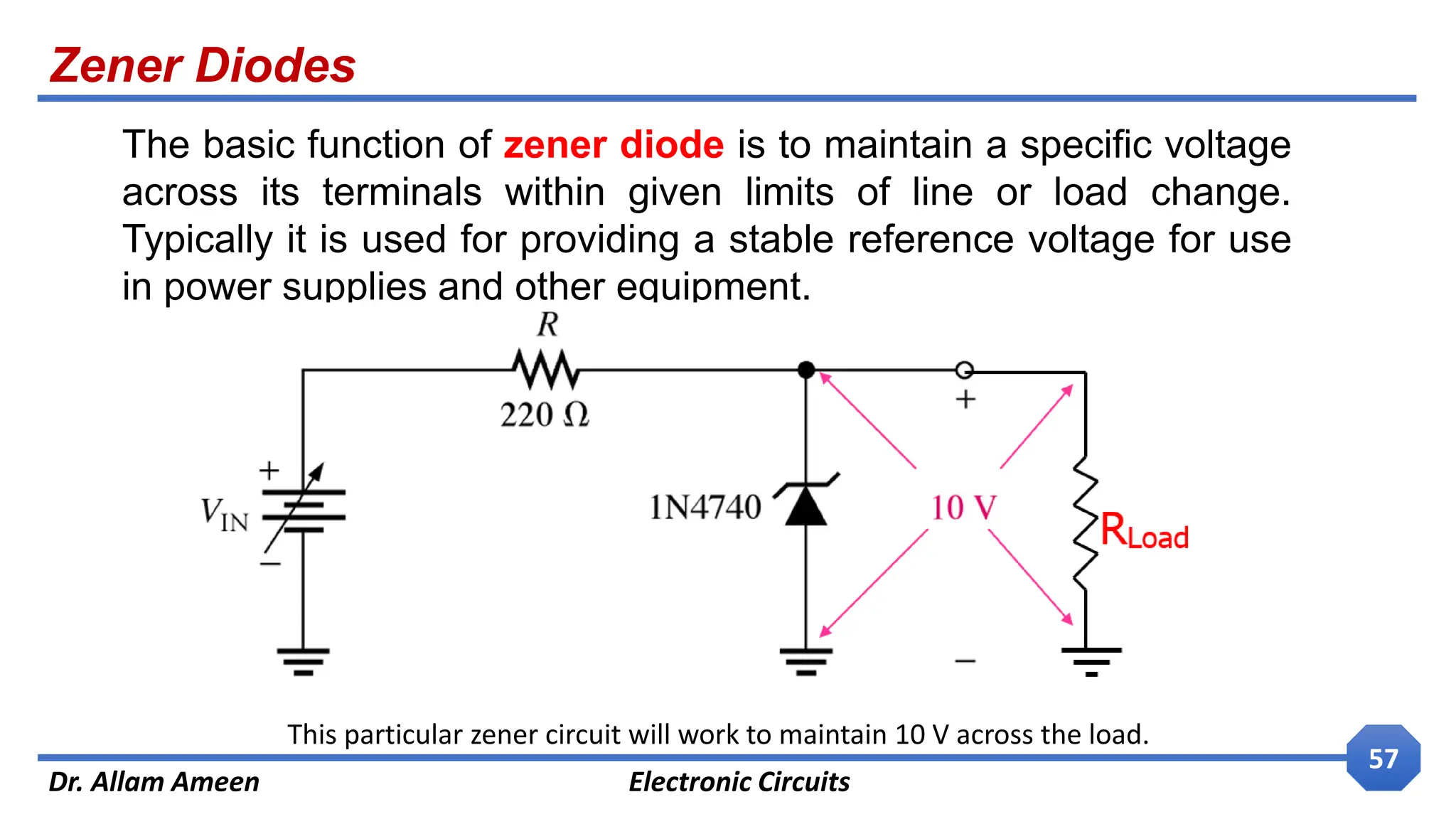
The basic function of zener diode is to maintain a specific voltage
across its terminals within given limits of line or load change.
Typically it is used for providing a stable reference voltage for use
in power supplies and other equipment.
This particular zener circuit will work to maintain 10 V across the load.
58.
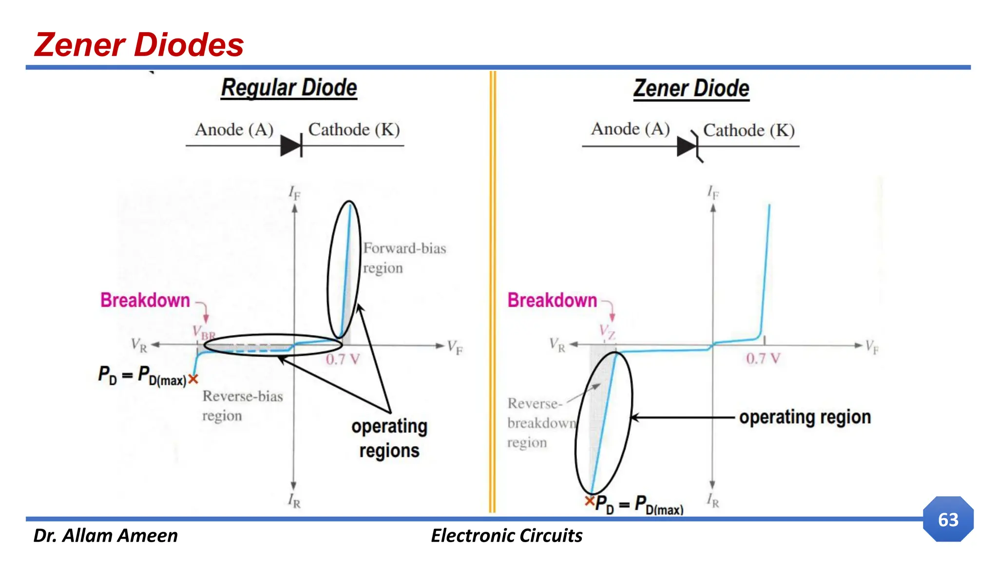
Zener Diodes
Dr. AllamAmeen Electronic Circuits
58
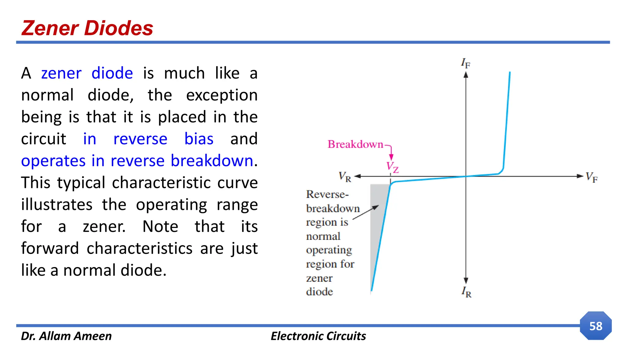
A zener diode is much like a
normal diode, the exception
being is that it is placed in the
circuit in reverse bias and
operates in reverse breakdown.
This typical characteristic curve
illustrates the operating range
for a zener. Note that its
forward characteristics are just
like a normal diode.
59.
Zener Diodes
Dr. AllamAmeen Electronic Circuits
59
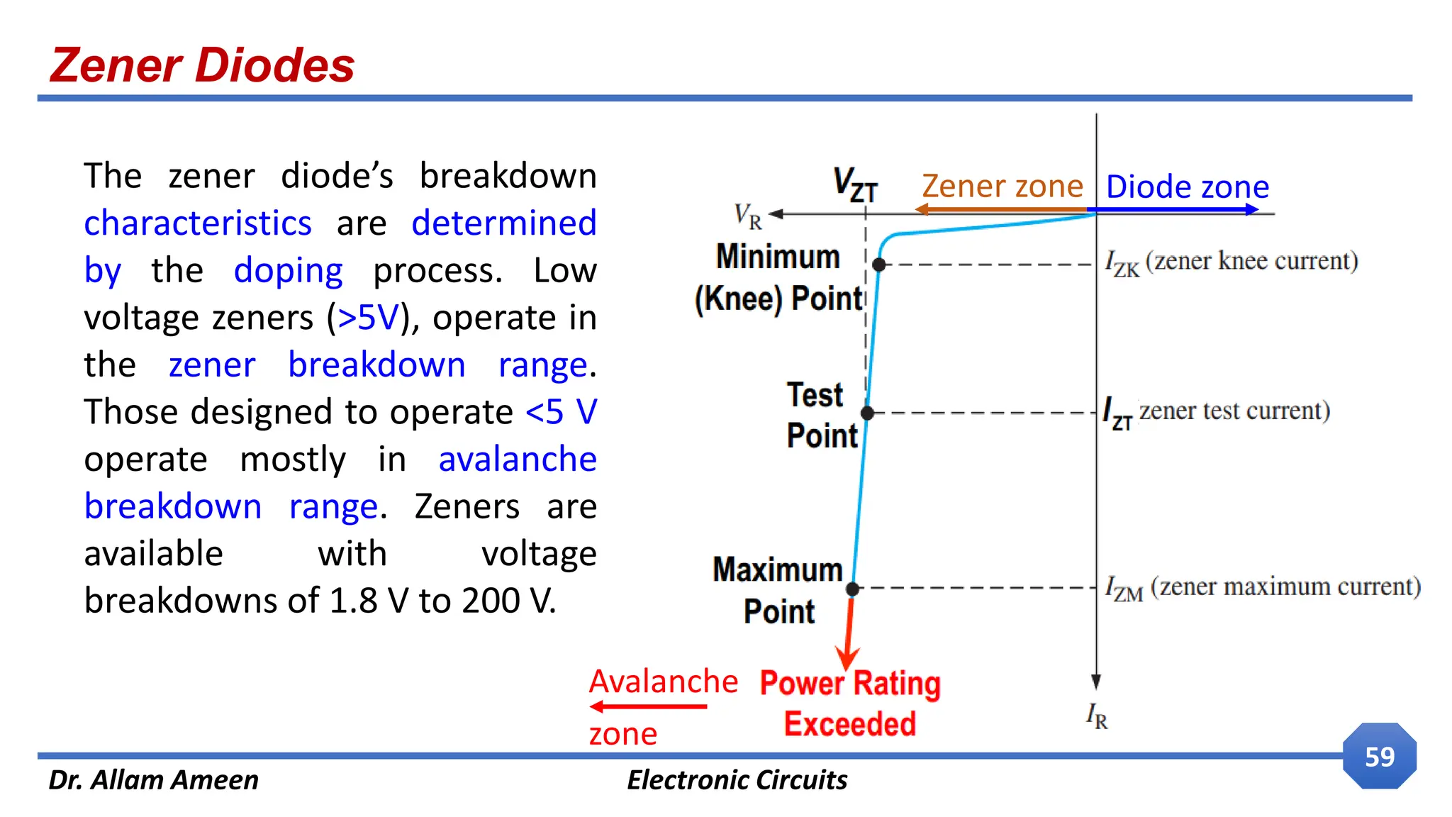
The zener diode’s breakdown
characteristics are determined
by the doping process. Low
voltage zeners (>5V), operate in
the zener breakdown range.
Those designed to operate <5 V
operate mostly in avalanche
breakdown range. Zeners are
available with voltage
breakdowns of 1.8 V to 200 V.
Zener zone Diode zone
Avalanche
zone
60.
Zener Diodes
Dr. AllamAmeen Electronic Circuits
60
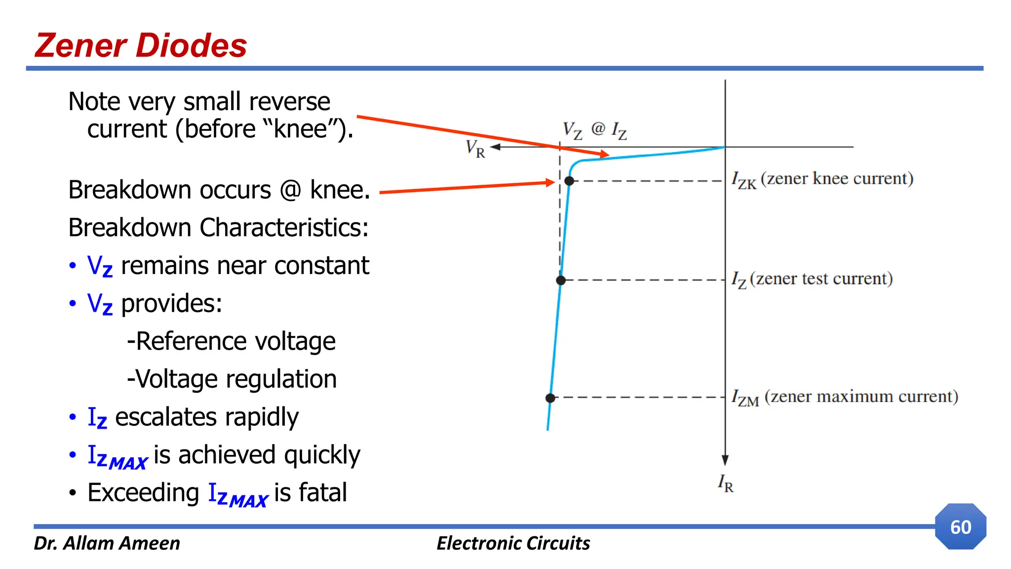
Note very small reverse
current (before “knee”).
Breakdown occurs @ knee.
Breakdown Characteristics:
• VZ remains near constant
• VZ provides:
-Reference voltage
-Voltage regulation
• IZ escalates rapidly
• IZMAX is achieved quickly
• Exceeding IZMAX is fatal
61.
Zener Diodes
Dr. AllamAmeen Electronic Circuits
61
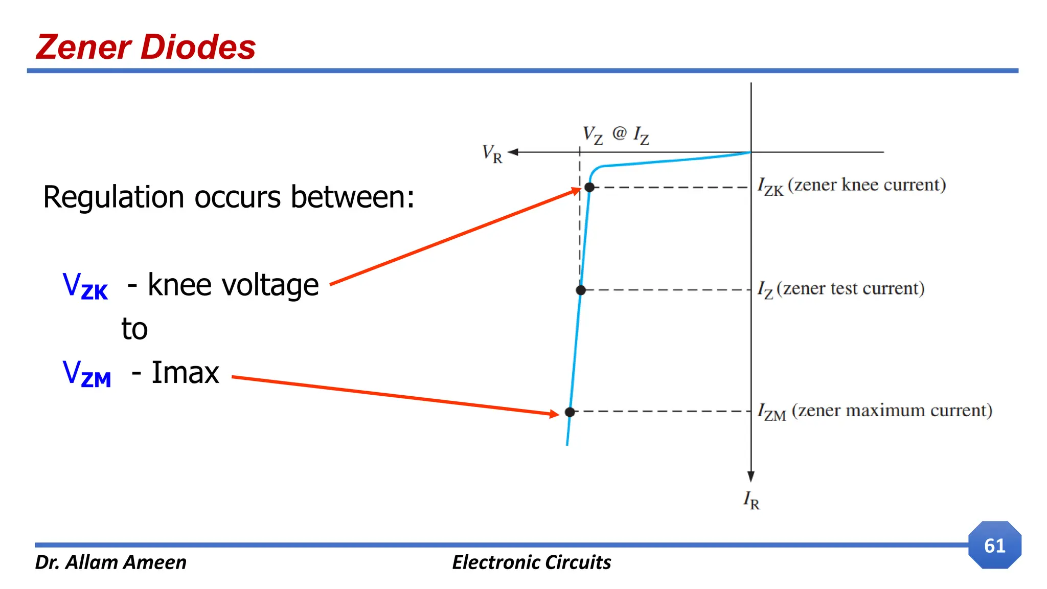
Regulation occurs between:
VZK - knee voltage
to
VZM - Imax
Zener Diodes
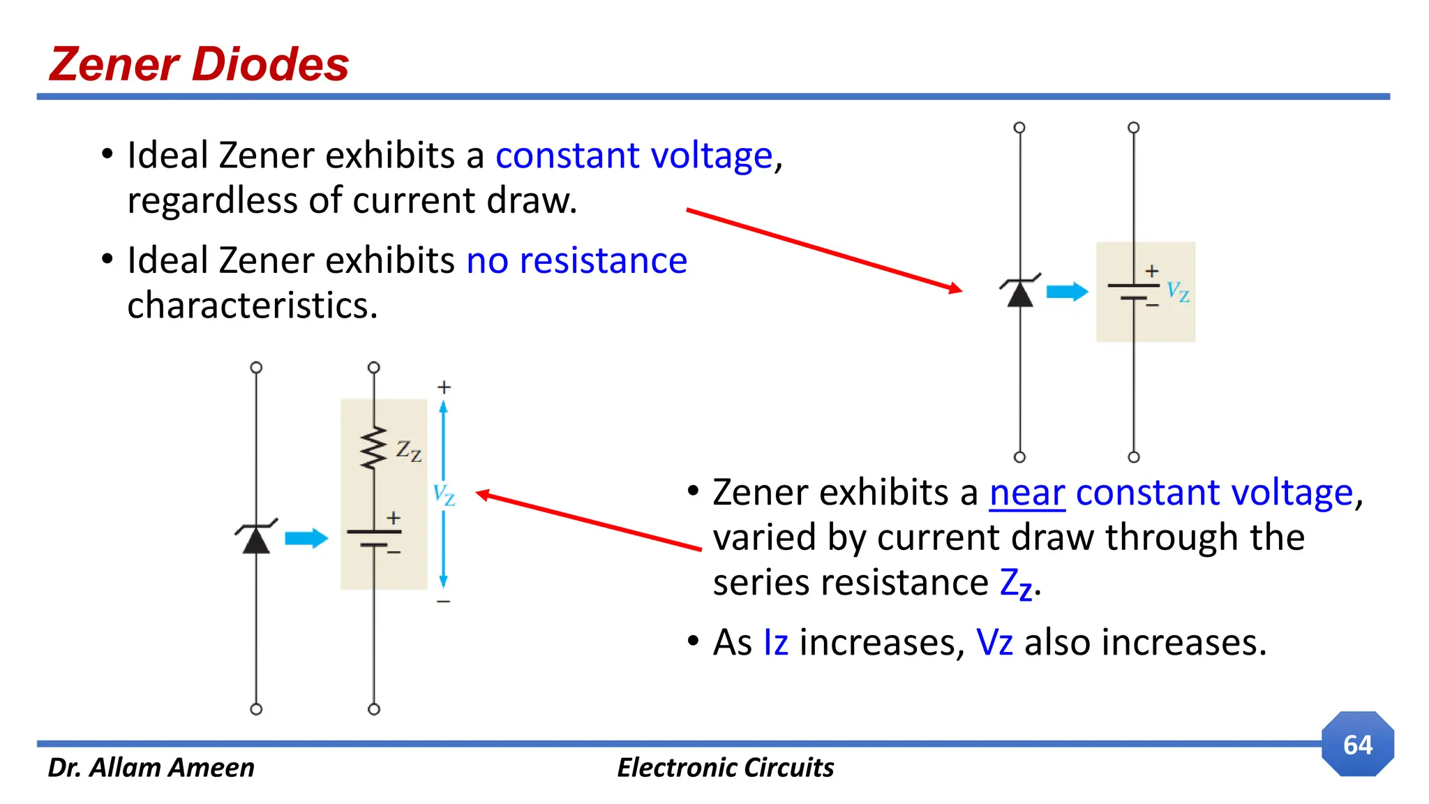
Dr. AllamAmeen Electronic Circuits
64
• Ideal Zener exhibits a constant voltage,
regardless of current draw.
• Ideal Zener exhibits no resistance
characteristics.
• Zener exhibits a near constant voltage,
varied by current draw through the
series resistance ZZ.
• As Iz increases, Vz also increases.
65.
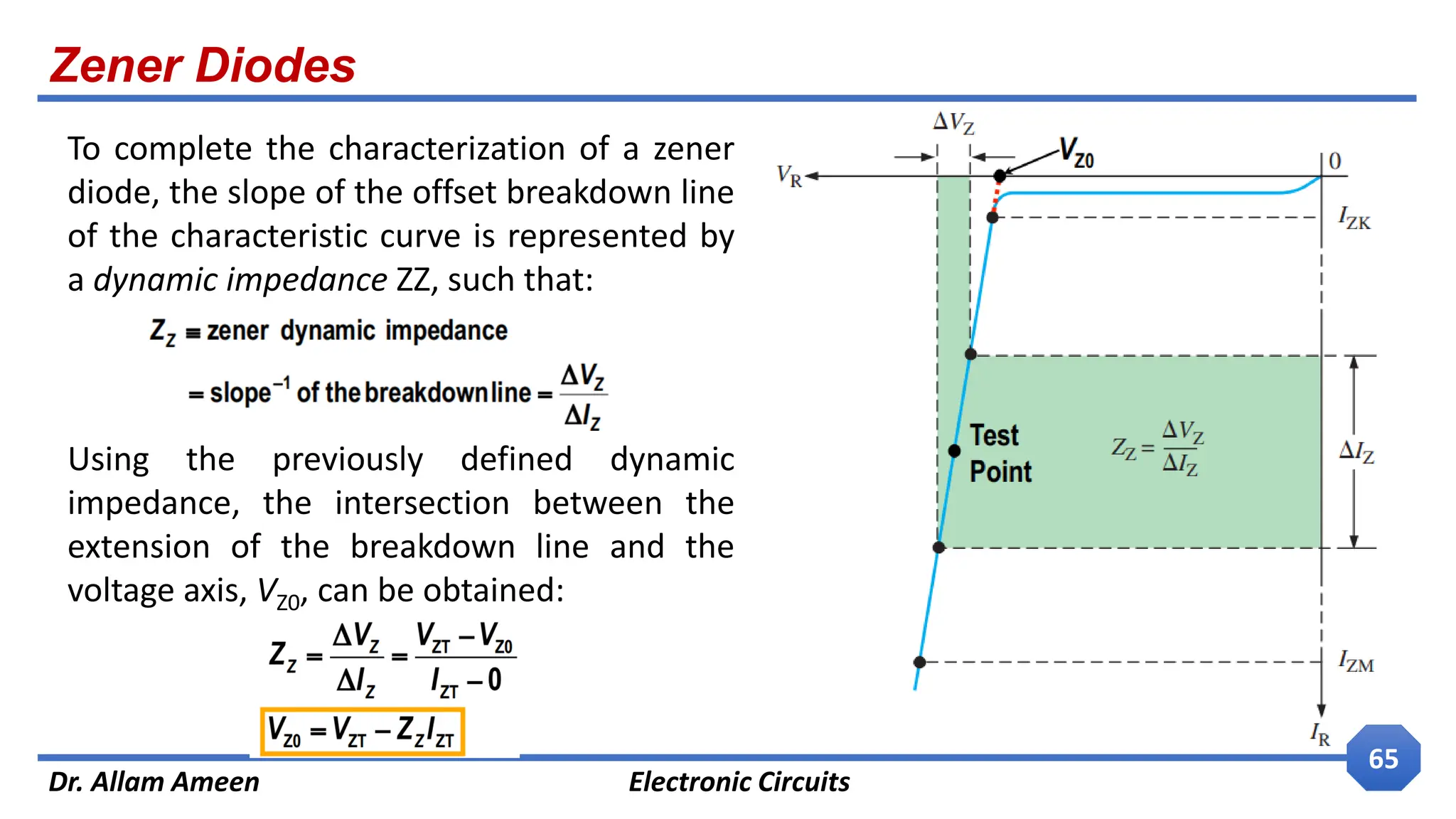
Zener Diodes
Dr. AllamAmeen Electronic Circuits
65
To complete the characterization of a zener
diode, the slope of the offset breakdown line
of the characteristic curve is represented by
a dynamic impedance ZZ, such that:
Using the previously defined dynamic
impedance, the intersection between the
extension of the breakdown line and the
voltage axis, VZ0, can be obtained:
Zener Diodes
Dr. AllamAmeen Electronic Circuits
67
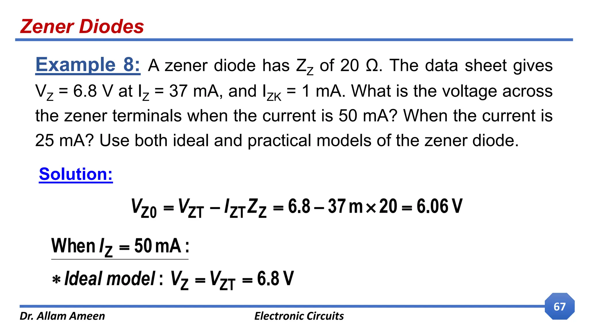
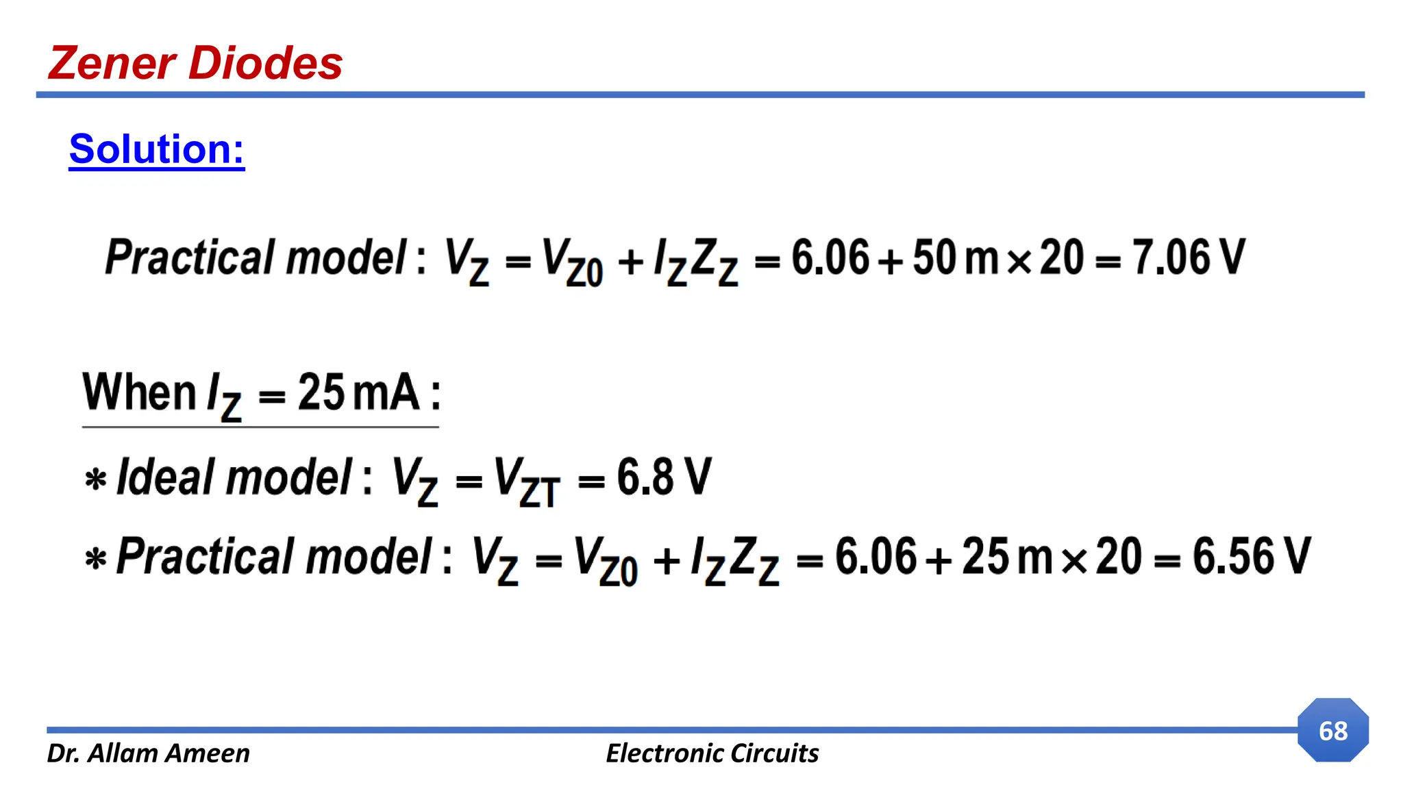
Example 8: A zener diode has ZZ of 20 Ω. The data sheet gives
VZ = 6.8 V at IZ = 37 mA, and IZK = 1 mA. What is the voltage across
the zener terminals when the current is 50 mA? When the current is
25 mA? Use both ideal and practical models of the zener diode.
Solution:
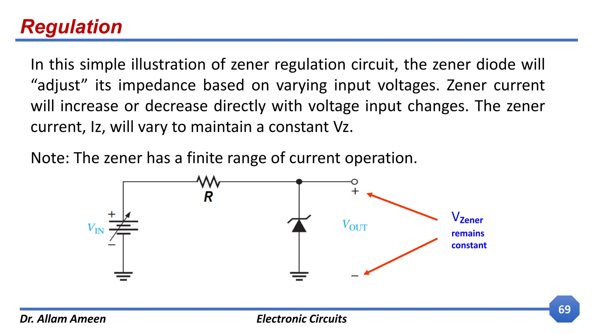
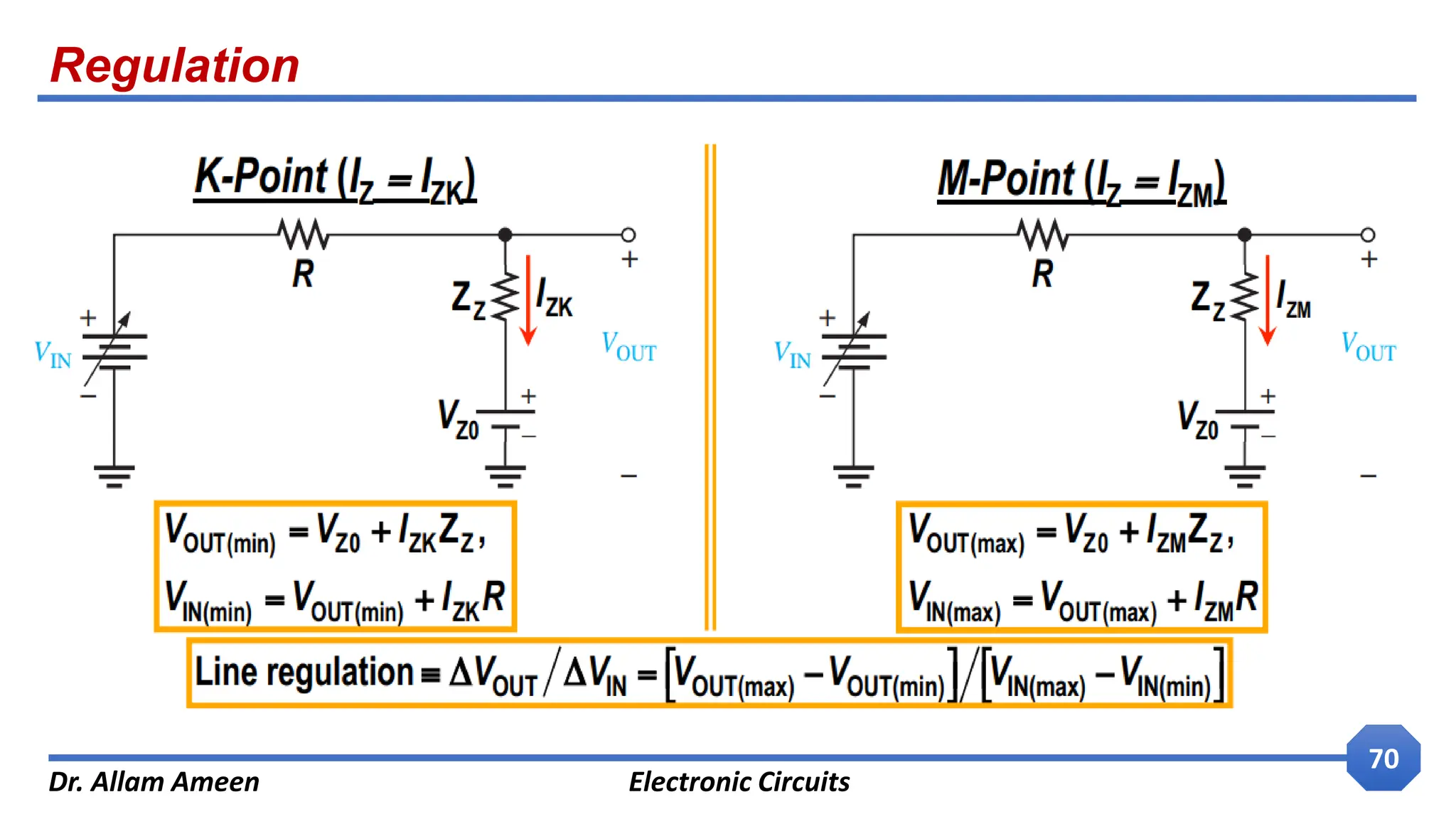
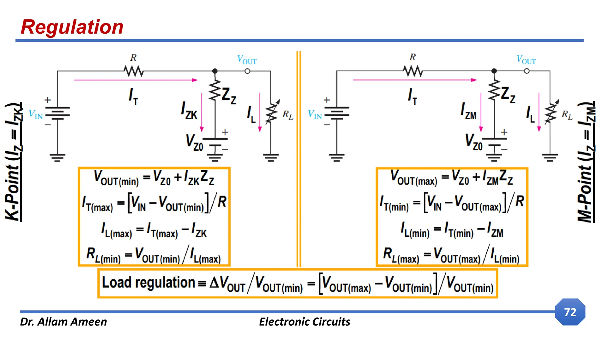
Regulation
Dr. Allam AmeenElectronic Circuits
69
In this simple illustration of zener regulation circuit, the zener diode will
“adjust” its impedance based on varying input voltages. Zener current
will increase or decrease directly with voltage input changes. The zener
current, Iz, will vary to maintain a constant Vz.
Note: The zener has a finite range of current operation.
VZener
remains
constant
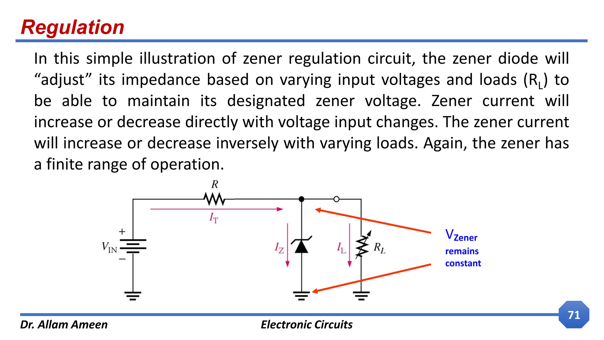
Regulation
Dr. Allam AmeenElectronic Circuits
71
In this simple illustration of zener regulation circuit, the zener diode will
“adjust” its impedance based on varying input voltages and loads (RL) to
be able to maintain its designated zener voltage. Zener current will
increase or decrease directly with voltage input changes. The zener current
will increase or decrease inversely with varying loads. Again, the zener has
a finite range of operation.
VZener
remains
constant
Regulation
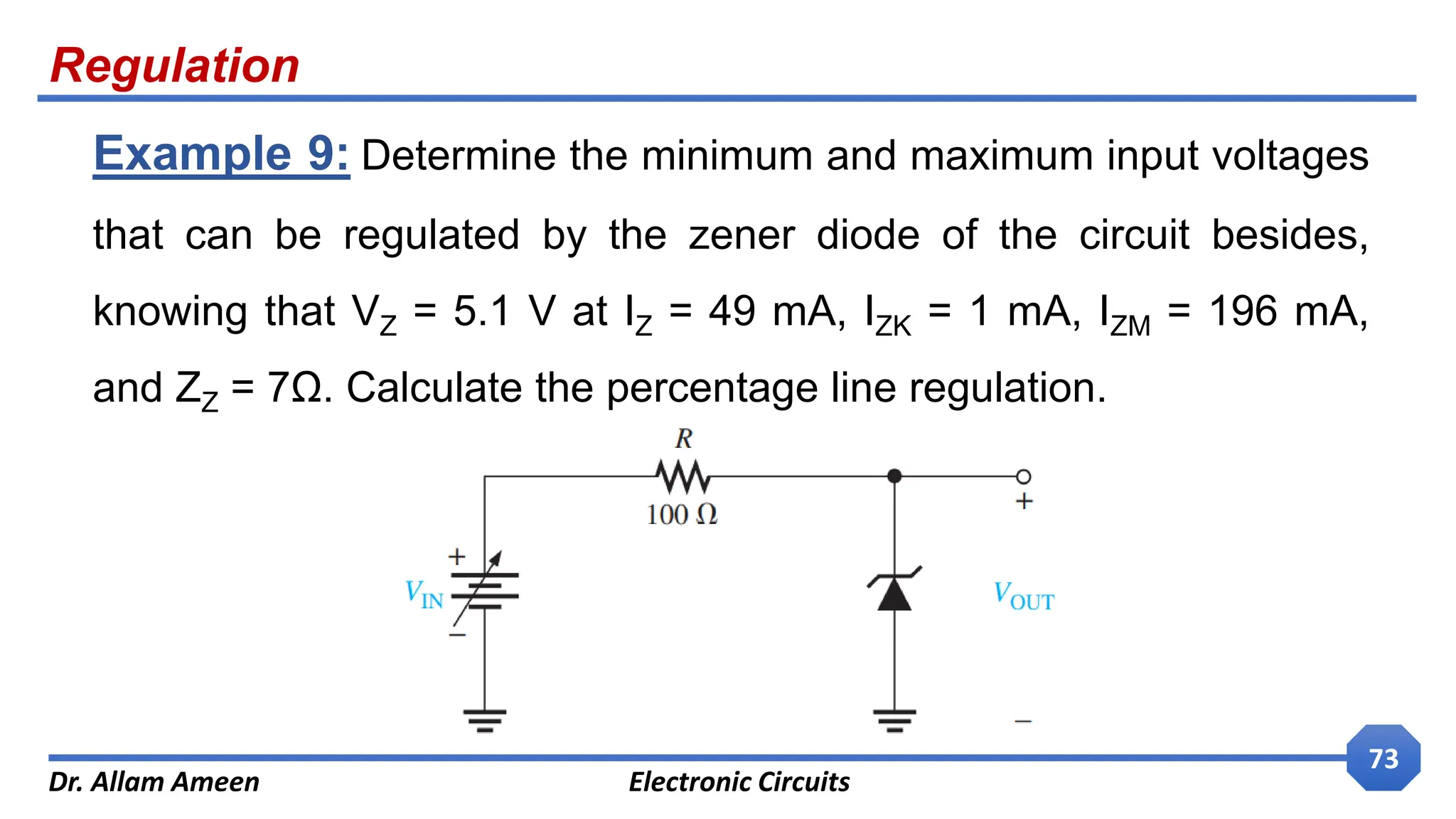
Dr. Allam AmeenElectronic Circuits
73
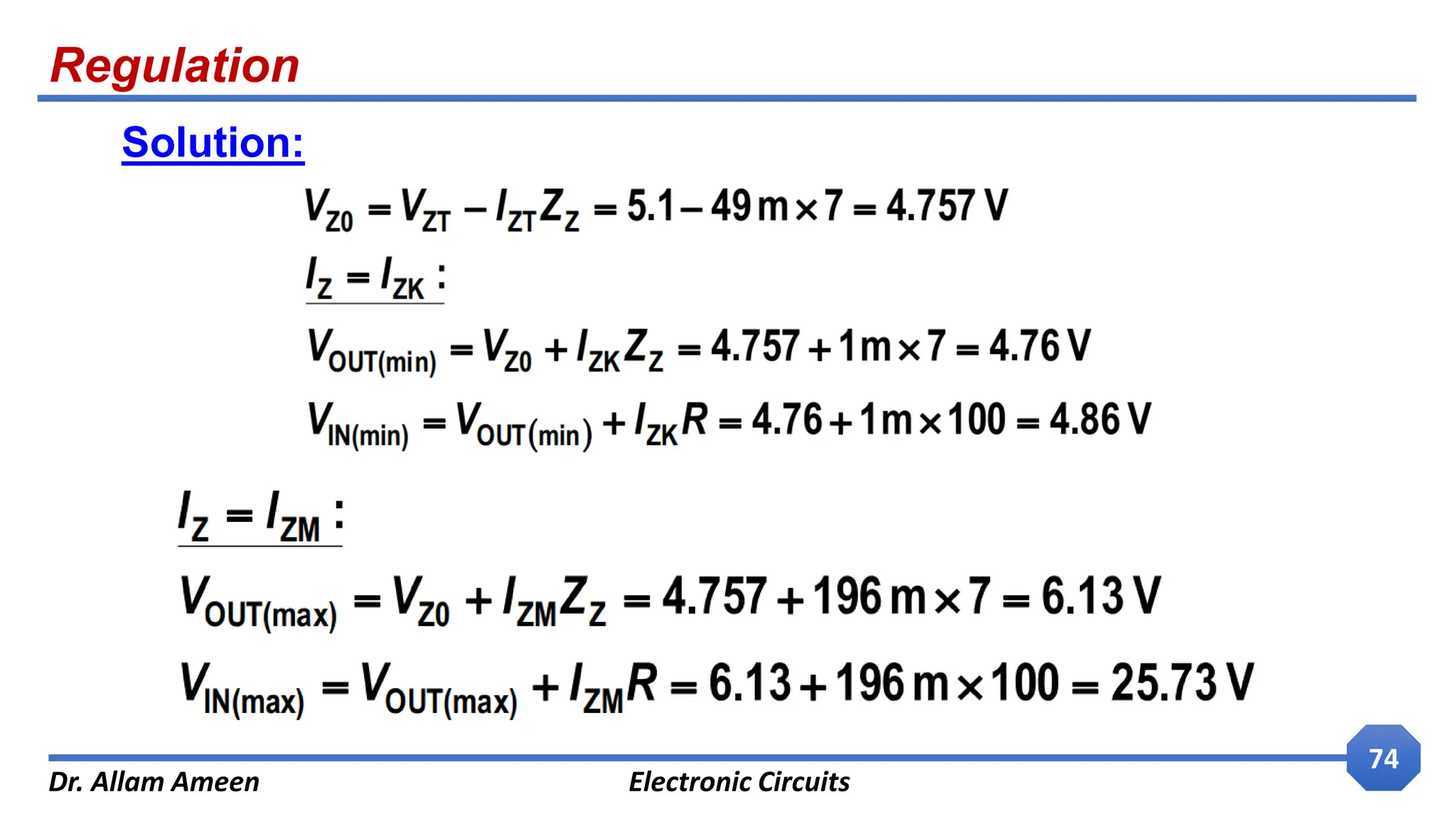
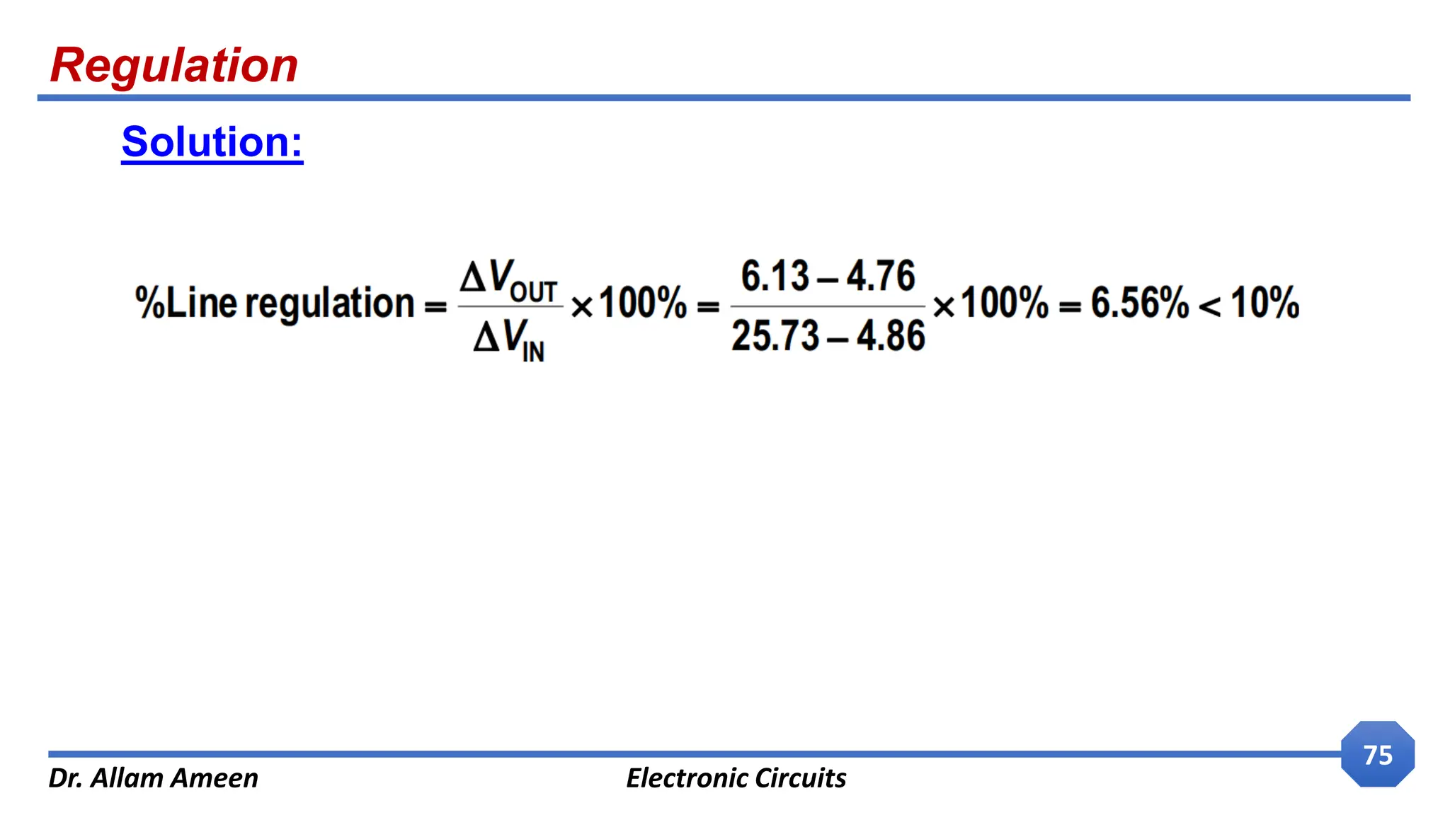
Example 9: Determine the minimum and maximum input voltages
that can be regulated by the zener diode of the circuit besides,
knowing that VZ = 5.1 V at IZ = 49 mA, IZK = 1 mA, IZM = 196 mA,
and ZZ = 7Ω. Calculate the percentage line regulation.
Regulation
Dr. Allam AmeenElectronic Circuits
76
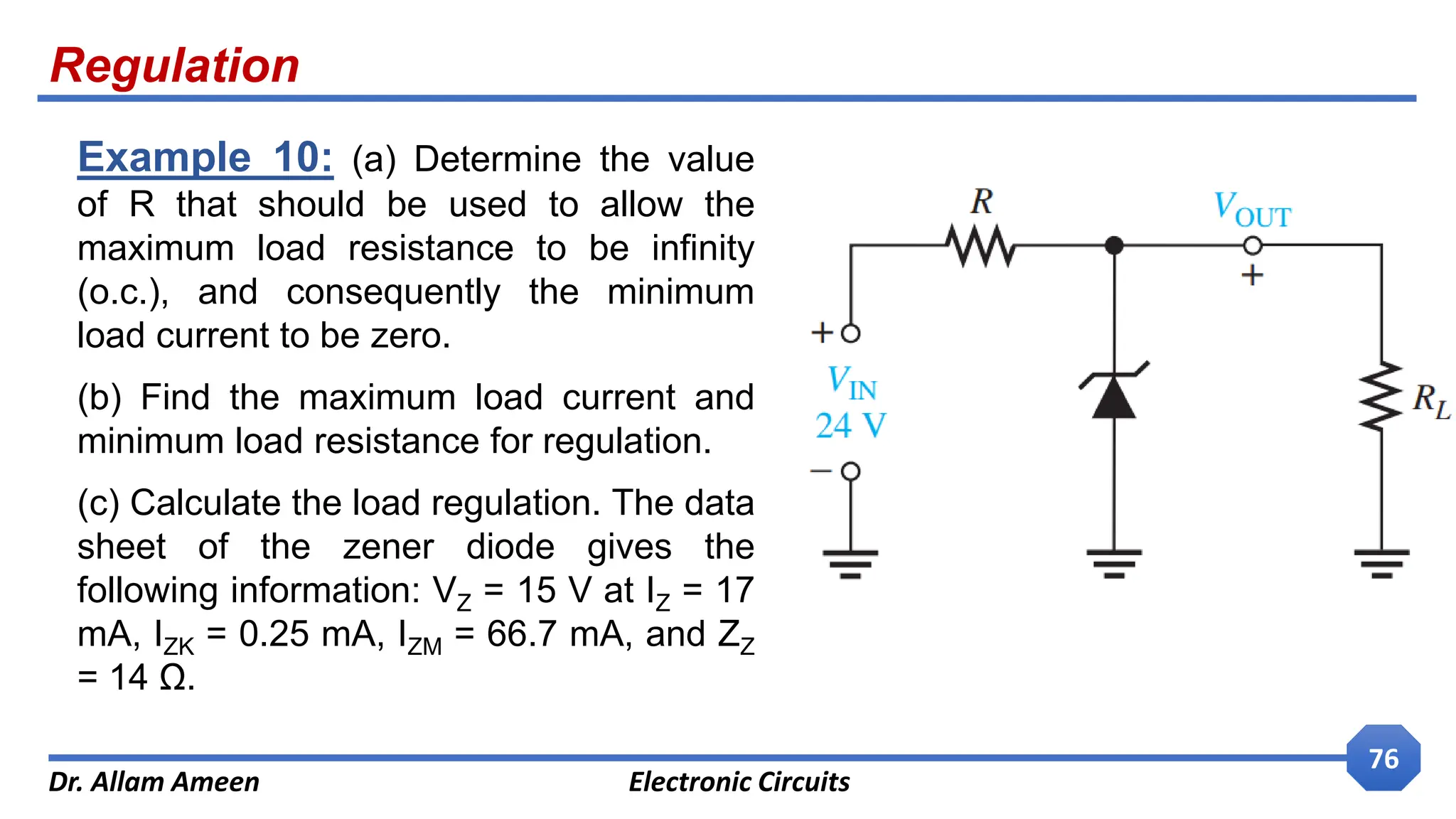
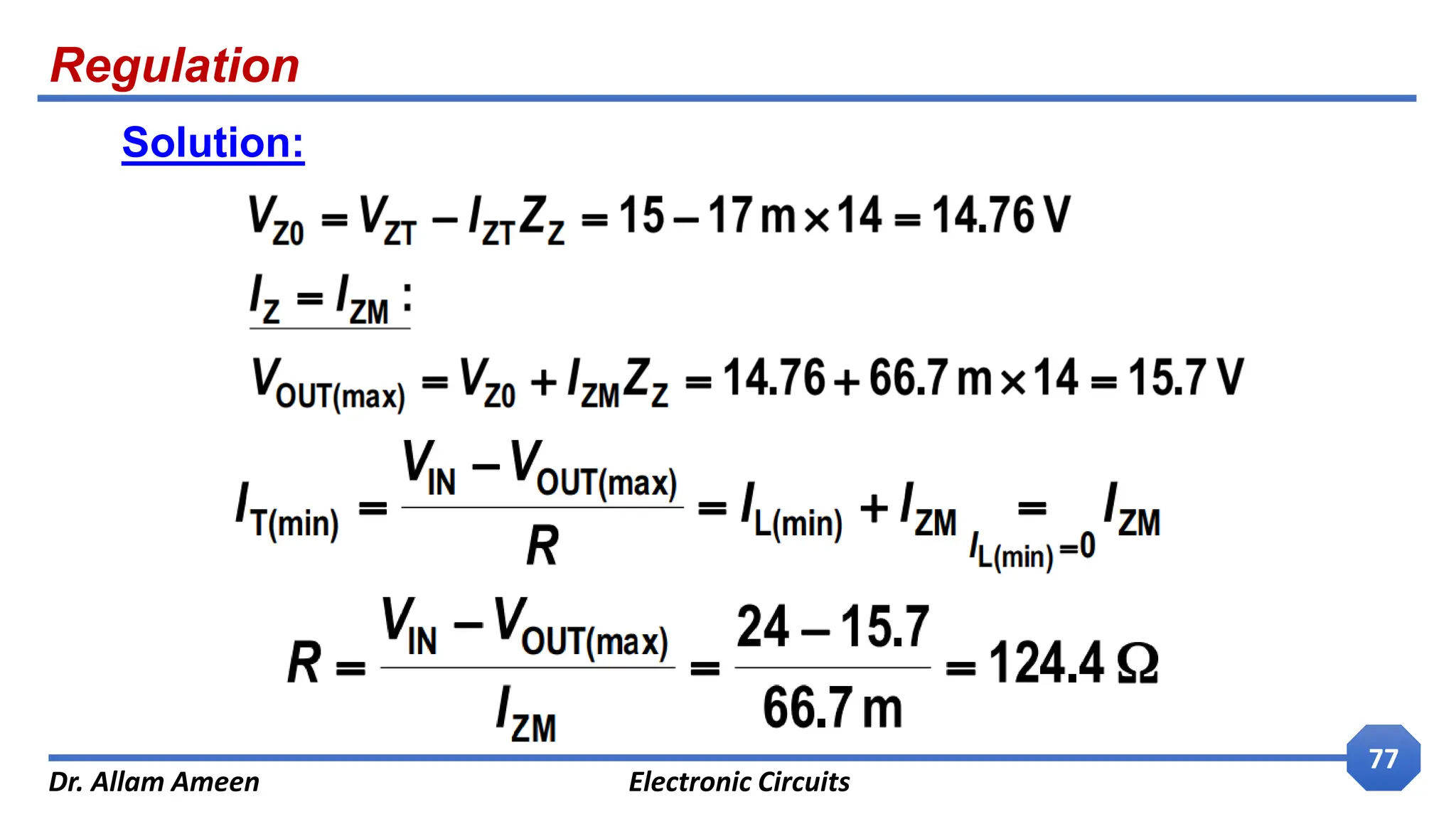
Example 10: (a) Determine the value
of R that should be used to allow the
maximum load resistance to be infinity
(o.c.), and consequently the minimum
load current to be zero.
(b) Find the maximum load current and
minimum load resistance for regulation.
(c) Calculate the load regulation. The data
sheet of the zener diode gives the
following information: VZ = 15 V at IZ = 17
mA, IZK = 0.25 mA, IZM = 66.7 mA, and ZZ
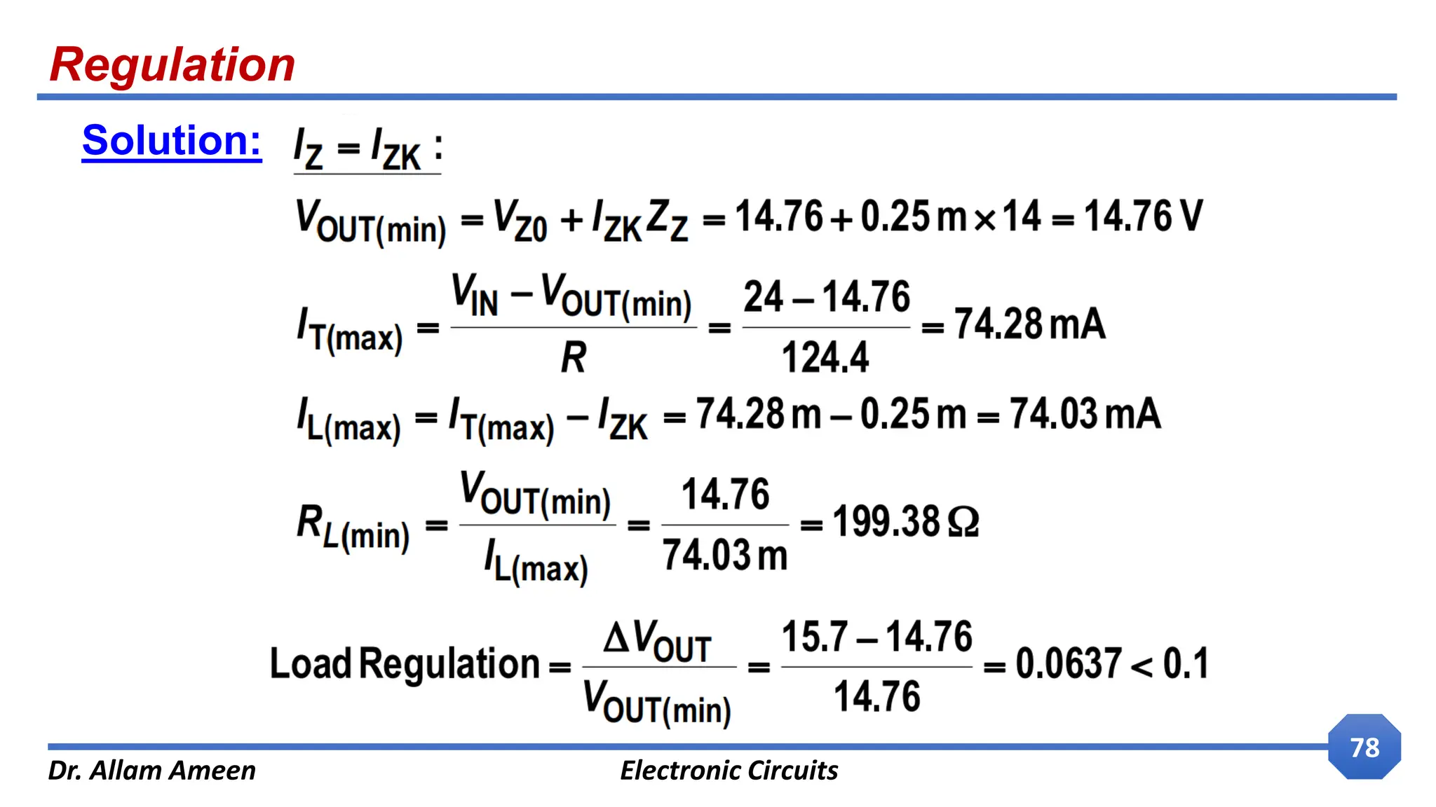
= 14 Ω.
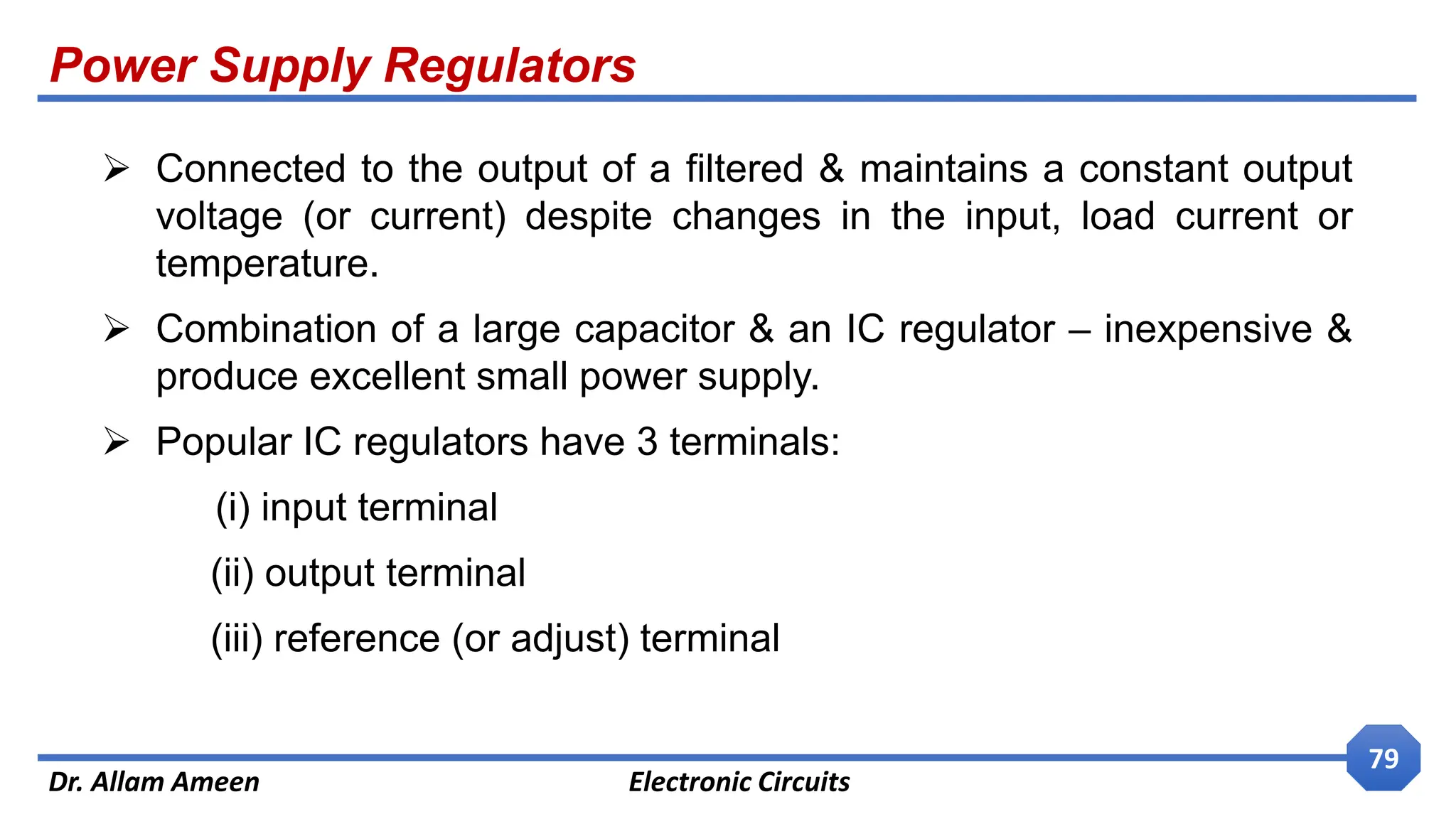
Power Supply Regulators
Dr.Allam Ameen Electronic Circuits
79
Connected to the output of a filtered & maintains a constant output
voltage (or current) despite changes in the input, load current or
temperature.
Combination of a large capacitor & an IC regulator – inexpensive &
produce excellent small power supply.
Popular IC regulators have 3 terminals:
(i) input terminal
(ii) output terminal
(iii) reference (or adjust) terminal
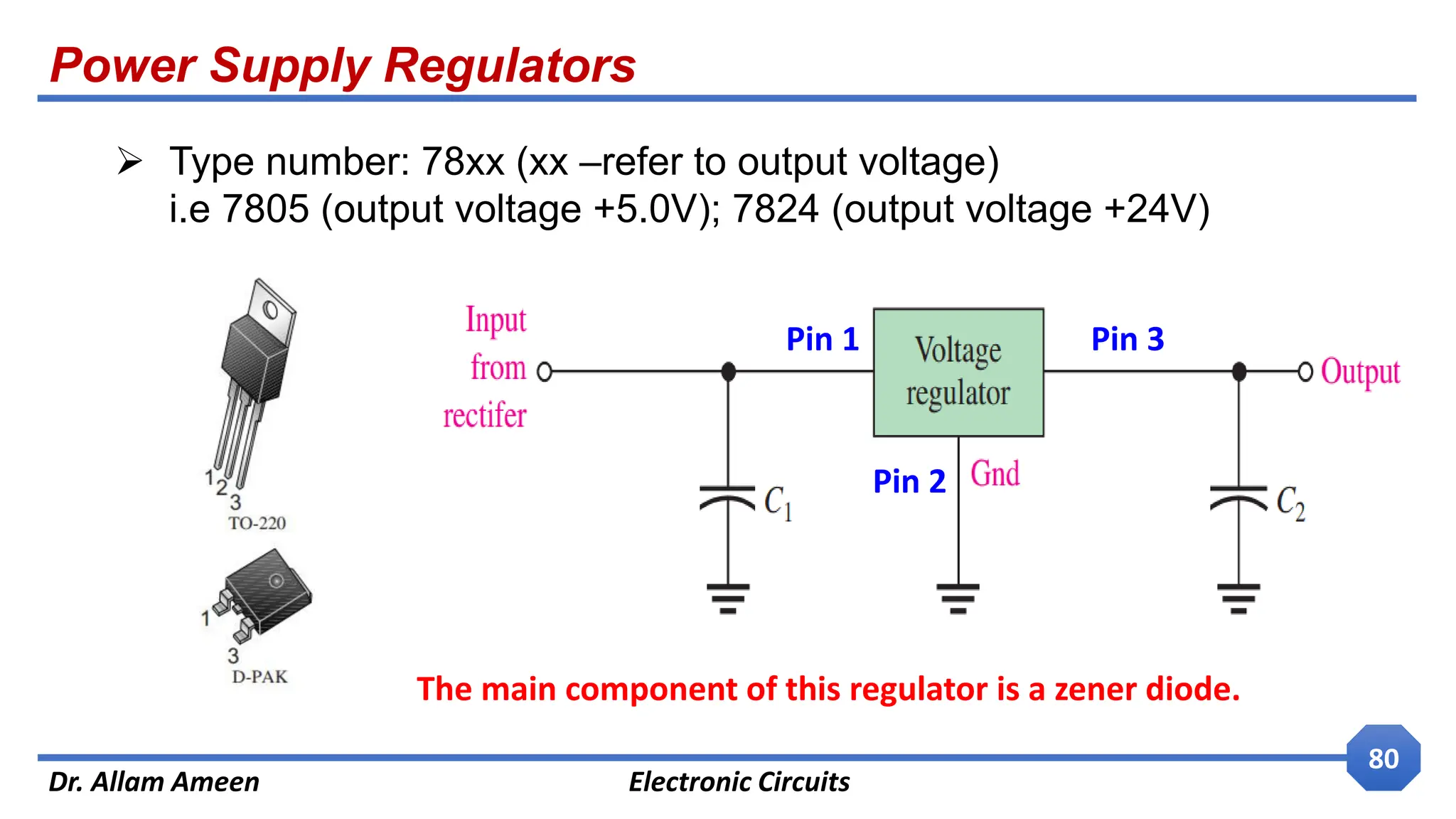
80.
Power Supply Regulators
Dr.Allam Ameen Electronic Circuits
80
Type number: 78xx (xx –refer to output voltage)
i.e 7805 (output voltage +5.0V); 7824 (output voltage +24V)
Pin 1
Pin 2
Pin 3
The main component of this regulator is a zener diode.
81.
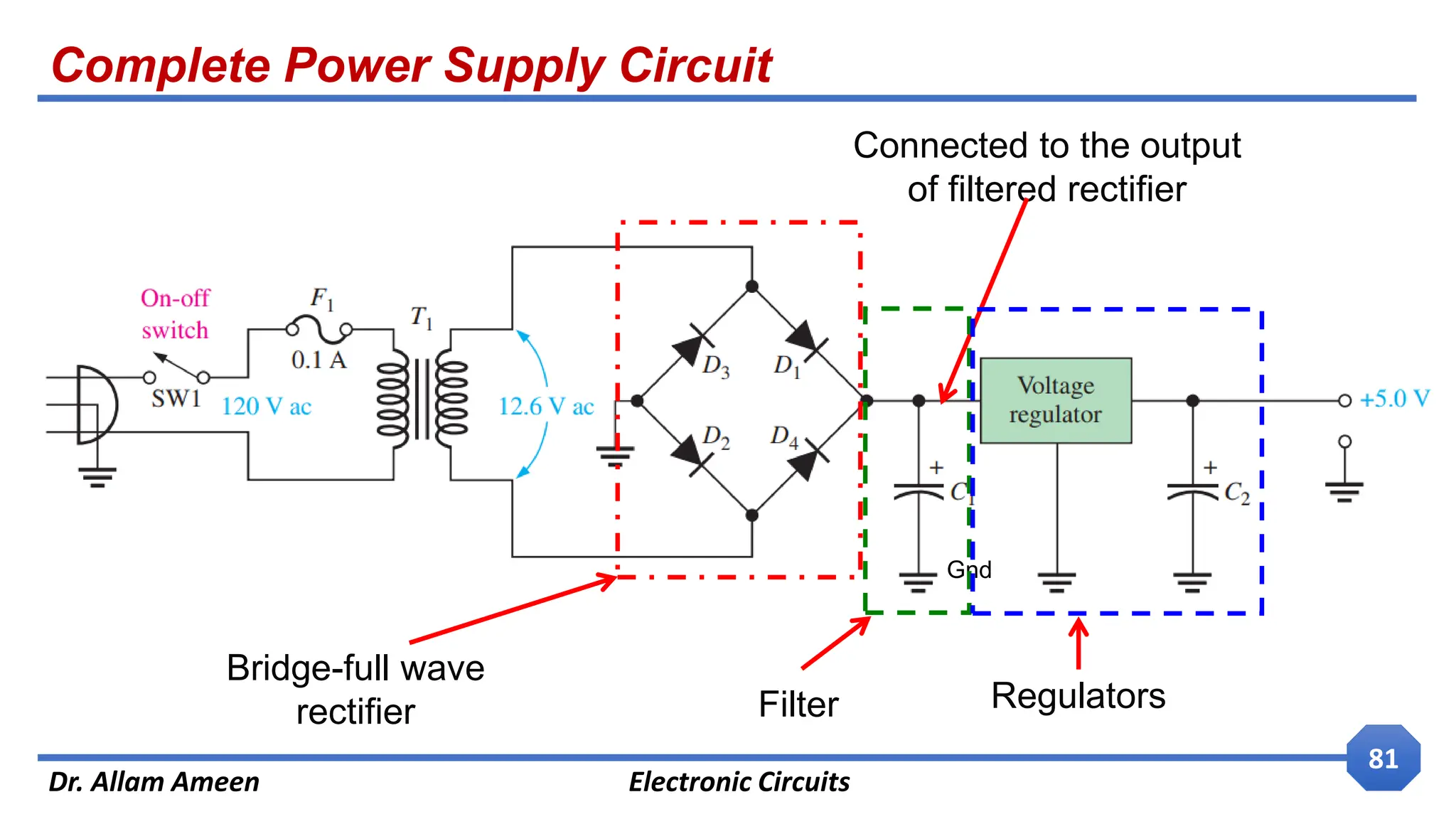
Complete Power SupplyCircuit
Dr. Allam Ameen Electronic Circuits
81
Gnd
Connected to the output
of filtered rectifier
Bridge-full wave
rectifier Filter Regulators
![Power Supply Filters
Dr. Allam Ameen Electronic Circuits
29
Lower ripple factor better filter [can be lowered by
increasing the value of filter capacitor or increasing the load
resistance]](https://image.slidesharecdn.com/lecture3-250327124641-a2d8bdb1/75/Lectures-in-electronic-circiuts-on-diode-29-2048.jpg)