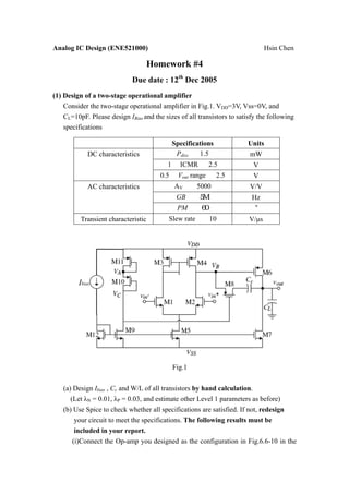
The document describes Homework #4 which involves designing a two-stage operational amplifier that meets various specifications. Students are asked to:
1) Design the op-amp by calculating component values to meet DC and AC specifications.
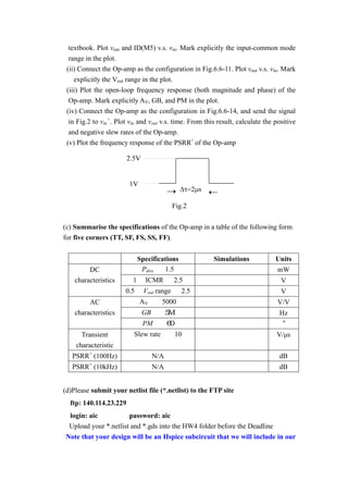
2) Use Spice simulation to verify the design meets specifications over temperature corners and generate plots of the input/output characteristics and frequency response.
3) Summarize the simulation results in a table showing whether specifications are met over process corners.
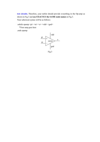
4) Submit the op-amp design as a Spice subcircuit for testing by the instructor. The subcircuit must use the node names shown in the figure.