Reprinted with permission from the February, 2015 issue of ...
One-Stop Turnkey PCB Fabrication
and Assembly: Rush PCB’s
Unique Approach
By Michael T. McGrath, Contributing Editor
I
n today’s world of electronics contract manufacturing, the
speed of fabricating PCBs and electronic assemblies is an
important factor, along with price, in maintaining a com-
petitive edge. Original equipment manufacturers (OEMs)
look to PCB fabrication and assem-
bly shops for fast turnaround times
but also for excellent value and high
performance in the fabricated elec-
tronic assemblies and PCBs. When
contract manufacturers can also
make it easier for OEM customers
to do business with them, whether
the OEM is attempting to sell elec-
tronic products for consumer, com-
mercial, industrial, or even military
markets, there is a better chance for
that business relationship to work
effectively.
For this reason, Roy Akber,
Chief Executive Officer (CEO) of
Rush PCB Inc., recently announced
a “soup-to-nuts” full turnkey PCB
assembly service: “People don’t
believe me at first when I tell them
that it’s as easy as e-mailing your
BOM, and includes a lot more than just the circuit assembly.”
Akber explains: “It’s a comprehensive way for customers to go
from concept to product to market in just a few easy steps. But
this has been our way of doing things since the very beginning.
We were founded in 1997, our business is to manufacture
boards from 2 to 32 layers, and then to provide quick turn con-
signed and full turnkey assemblies.” Rush PCB Inc. specializes
in high-layer-count PCBs, engineering prototypes, and EMS.
According to Akber: “We realized early on that customers
did not want to go to multiple sources to get their assemblies
built. There are logistical issues, time and delivery, traceabili-
ty issues. So we have set up an intuitive system whereby you
can literally upload your BOM file and you’ll get a full turnkey
price for components, labor and bare boards.” He adds: “We do
the leg-work for you. We will find PCB parts pricing, and all
other vital data including suggested substitute parts from mul-
tiple electronic distributors. We will
list all in detail and compute the
most optimized quantity/price selec-
tion based on your job.” The advan-
tage of doing it this way, he says, is
simply that it helps maintain control
of the product: “That means that we
can save costs for the customer,
speed its development, and also
ensure quality and long-term relia-
bility. Our design and manufacturing
engineers are here and available to
the customer every step along the
way. That is a tremendous help to
the customer.”
Procurement Specialists
Rush PCB Inc. has the capabil-
ity to start with a customer’s design
and provide a completed product at
a competitive cost and quick turn-
around time. Akber notes: “Our team of procurement special-
ists scours their sources to find you the exact part you are
looking for, at the best price that is out in the market on any
given day. In addition, our teams of process engineers and
line operators have the ability to take your most complex
project and turn it around for you within a single day.”
The wide range of additional services and capabilities in
the “turnkey solution” that Akber announced include PCB
design and design-for-manufacturability (DFM) engineering
assistance, to help make sure that the layout will work prop-
erly in the assembly and manufacturing process. Rush PCB
Inc. also provides inspection and test, and beyond, including
ELECTRONIC MFG. SERVICES (EMS)
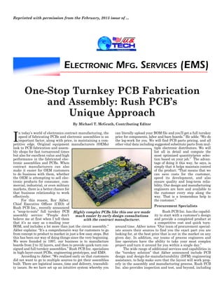
Highly complex PCBs like this one are made
much easier by early design consultations
with the contract manufacturer.
box build and final assembly if required or desired. Akber
offers that “our staff engineers work with you, our customer,
throughout the initial design and development process to
assure manufacturability, product quality, and consistency.”
Recently, Rush PCB announced that it offers some spe-
cialized expertise in challenging multilayer circuit board
structures including blind, buried viaholes, and economical,
fast laser drilling which is particularly applicable to stacked
microvia drilling for multilayer circuit boards.
Shiva Dantu, a senior manufacturing engineer at Rush
PCB Inc., with more than 25 years in electronics manufactur-
ing experience, volunteers: “With our
precision laser drilling capability, we
can process 4-mil microvias, for
example, and blind or buried vias
and more.”
Dantu explains: “We handle
these challenging features by using
well-developed techniques and
layer-by-layer fabrication methods
that we have learned or developed
over time. Blind vias originate on an
outer layer but terminate at an
inner layer; buried vias exist only
between inner layers and do not
begin or terminate on an outer
layer, so they must be drilled while
layers are being added to the PCB
rather than when it is finished.”
Blind and Buried Vias
Dantu adds: “Blind and buried
vias help save PCB real estate by allowing features and lines
to be designed above or below them without making a connec-
tion. This helps our customers build more compact assem-
blies. Many of today’s fine-pitch BGA and flip-chip component
footprints do not allow for running traces. Instead, the blind
and buried vias will only connect those layers that are
required to have a connection in that specific area, allowing
for PCB real estate space savings.”
For the highest possible circuit board routing density,
stacked microvias, compound structures, are stacked one on
top of another. Laser-drilled microvias consume less board
real estate than mechanical through-the-board vias.
Microvias, having been drilled by laser, are smaller in diam-
eter than through-the-board vias, allowing more space to be
devoted to circuit traces. A microvia links only one layer of
foil to the next, so that circuit layers above and below are
available for additional foil lines to further increase the over-
all circuit density.
Rush PCB can fabricate stacked-microvia, high-density-
interconnector (HDI) circuit boards to 48 layers, working with
standard and oversized circuit boards.
The firm’s 4-mil-diameter laser-drilling capability
allows for fine features to be produced, according to Dantu.
“But we emphasize that we can help customers with these
types of space-saving features if they come to us at the begin-
ning of the design stage for their product,” he said. “We pro-
vide a full spectrum of engineering and design support, and
can help customers find more economical ways to do certain
things, such as impedance control.
We have ready-to-go proven designs
in house that can be immediately
applied to a customer’s needs. Our
goal is ultimate reliability for the
customer’s products.”
Engineering assistance can
make the difference between a prod-
uct that develops smoothly, and one
that has nothing but problems along
the way. Dantu explains: “Quite fre-
quently, customers, especially those
who have worked with us before,
will come to us during the design
stage with a new product that they
want us to build for them. They are
looking for design or DFM help so
that their product will have a suc-
cessful launch. They will start by
telling us that this is something
that they are planning to do, and
they may be looking at different applications, and perhaps a
more economical method of doing things.” He adds:
“Remember that we also have already some ready-to-adapt
successful designs on board, for such things as impedance
control and more. Once their product goes to manufacturing,
their board should not have any issues, particularly none
relating to reliability. It is always much better to conduct
this process in the beginning, during the planning stages,
rather than later on when the customer is already done with
the files! Because then the customer has to go and redo it,
which is very much a waste of time for the customer and for
us, and because of delays and re-do, the price can then be
higher. So it is most beneficial when the customer comes to
us during the design stage.”
Contact: Rush PCB Inc., 2151-20 O’Toole Avenue,
San Jose, CA 95131  408-496-6013 fax: 408-854-8094
E-mail: sales@rushocb.com Web: www.rushpcb.com 
www.us-tech.com
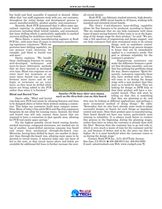
Smaller PCBs have their own issues,
such as the thru-hole vias on this board.

EMS RUSH PCB

  • 1.
    Reprinted with permissionfrom the February, 2015 issue of ... One-Stop Turnkey PCB Fabrication and Assembly: Rush PCB’s Unique Approach By Michael T. McGrath, Contributing Editor I n today’s world of electronics contract manufacturing, the speed of fabricating PCBs and electronic assemblies is an important factor, along with price, in maintaining a com- petitive edge. Original equipment manufacturers (OEMs) look to PCB fabrication and assem- bly shops for fast turnaround times but also for excellent value and high performance in the fabricated elec- tronic assemblies and PCBs. When contract manufacturers can also make it easier for OEM customers to do business with them, whether the OEM is attempting to sell elec- tronic products for consumer, com- mercial, industrial, or even military markets, there is a better chance for that business relationship to work effectively. For this reason, Roy Akber, Chief Executive Officer (CEO) of Rush PCB Inc., recently announced a “soup-to-nuts” full turnkey PCB assembly service: “People don’t believe me at first when I tell them that it’s as easy as e-mailing your BOM, and includes a lot more than just the circuit assembly.” Akber explains: “It’s a comprehensive way for customers to go from concept to product to market in just a few easy steps. But this has been our way of doing things since the very beginning. We were founded in 1997, our business is to manufacture boards from 2 to 32 layers, and then to provide quick turn con- signed and full turnkey assemblies.” Rush PCB Inc. specializes in high-layer-count PCBs, engineering prototypes, and EMS. According to Akber: “We realized early on that customers did not want to go to multiple sources to get their assemblies built. There are logistical issues, time and delivery, traceabili- ty issues. So we have set up an intuitive system whereby you can literally upload your BOM file and you’ll get a full turnkey price for components, labor and bare boards.” He adds: “We do the leg-work for you. We will find PCB parts pricing, and all other vital data including suggested substitute parts from mul- tiple electronic distributors. We will list all in detail and compute the most optimized quantity/price selec- tion based on your job.” The advan- tage of doing it this way, he says, is simply that it helps maintain control of the product: “That means that we can save costs for the customer, speed its development, and also ensure quality and long-term relia- bility. Our design and manufacturing engineers are here and available to the customer every step along the way. That is a tremendous help to the customer.” Procurement Specialists Rush PCB Inc. has the capabil- ity to start with a customer’s design and provide a completed product at a competitive cost and quick turn- around time. Akber notes: “Our team of procurement special- ists scours their sources to find you the exact part you are looking for, at the best price that is out in the market on any given day. In addition, our teams of process engineers and line operators have the ability to take your most complex project and turn it around for you within a single day.” The wide range of additional services and capabilities in the “turnkey solution” that Akber announced include PCB design and design-for-manufacturability (DFM) engineering assistance, to help make sure that the layout will work prop- erly in the assembly and manufacturing process. Rush PCB Inc. also provides inspection and test, and beyond, including ELECTRONIC MFG. SERVICES (EMS) Highly complex PCBs like this one are made much easier by early design consultations with the contract manufacturer.
  • 2.
    box build andfinal assembly if required or desired. Akber offers that “our staff engineers work with you, our customer, throughout the initial design and development process to assure manufacturability, product quality, and consistency.” Recently, Rush PCB announced that it offers some spe- cialized expertise in challenging multilayer circuit board structures including blind, buried viaholes, and economical, fast laser drilling which is particularly applicable to stacked microvia drilling for multilayer circuit boards. Shiva Dantu, a senior manufacturing engineer at Rush PCB Inc., with more than 25 years in electronics manufactur- ing experience, volunteers: “With our precision laser drilling capability, we can process 4-mil microvias, for example, and blind or buried vias and more.” Dantu explains: “We handle these challenging features by using well-developed techniques and layer-by-layer fabrication methods that we have learned or developed over time. Blind vias originate on an outer layer but terminate at an inner layer; buried vias exist only between inner layers and do not begin or terminate on an outer layer, so they must be drilled while layers are being added to the PCB rather than when it is finished.” Blind and Buried Vias Dantu adds: “Blind and buried vias help save PCB real estate by allowing features and lines to be designed above or below them without making a connec- tion. This helps our customers build more compact assem- blies. Many of today’s fine-pitch BGA and flip-chip component footprints do not allow for running traces. Instead, the blind and buried vias will only connect those layers that are required to have a connection in that specific area, allowing for PCB real estate space savings.” For the highest possible circuit board routing density, stacked microvias, compound structures, are stacked one on top of another. Laser-drilled microvias consume less board real estate than mechanical through-the-board vias. Microvias, having been drilled by laser, are smaller in diam- eter than through-the-board vias, allowing more space to be devoted to circuit traces. A microvia links only one layer of foil to the next, so that circuit layers above and below are available for additional foil lines to further increase the over- all circuit density. Rush PCB can fabricate stacked-microvia, high-density- interconnector (HDI) circuit boards to 48 layers, working with standard and oversized circuit boards. The firm’s 4-mil-diameter laser-drilling capability allows for fine features to be produced, according to Dantu. “But we emphasize that we can help customers with these types of space-saving features if they come to us at the begin- ning of the design stage for their product,” he said. “We pro- vide a full spectrum of engineering and design support, and can help customers find more economical ways to do certain things, such as impedance control. We have ready-to-go proven designs in house that can be immediately applied to a customer’s needs. Our goal is ultimate reliability for the customer’s products.” Engineering assistance can make the difference between a prod- uct that develops smoothly, and one that has nothing but problems along the way. Dantu explains: “Quite fre- quently, customers, especially those who have worked with us before, will come to us during the design stage with a new product that they want us to build for them. They are looking for design or DFM help so that their product will have a suc- cessful launch. They will start by telling us that this is something that they are planning to do, and they may be looking at different applications, and perhaps a more economical method of doing things.” He adds: “Remember that we also have already some ready-to-adapt successful designs on board, for such things as impedance control and more. Once their product goes to manufacturing, their board should not have any issues, particularly none relating to reliability. It is always much better to conduct this process in the beginning, during the planning stages, rather than later on when the customer is already done with the files! Because then the customer has to go and redo it, which is very much a waste of time for the customer and for us, and because of delays and re-do, the price can then be higher. So it is most beneficial when the customer comes to us during the design stage.” Contact: Rush PCB Inc., 2151-20 O’Toole Avenue, San Jose, CA 95131  408-496-6013 fax: 408-854-8094 E-mail: sales@rushocb.com Web: www.rushpcb.com  www.us-tech.com Smaller PCBs have their own issues, such as the thru-hole vias on this board.