This document provides standards for high-reliability soldering of surface-mount and mixed technology assemblies. It covers topics such as process identification documents, material selection, soldering procedures, cleaning, inspection criteria, quality assurance requirements, and verification testing. The document establishes workmanship illustrations and acceptance criteria to help ensure soldered connections meet reliability needs for space applications.


![ECSS‐Q‐ST‐70‐38C
31 July 2008
4
Principles of reliable soldered connections
The following are the general principles to ensure reliable soldered connections:
• Reliable soldered connections are the result of proper design, control of
tools, materials, processes and work environments, and workmanship
performed in accordance to verified and approved procedures,
inspection control and precautions.
• The basic design concepts to ensure reliable connections and to avoid
solder joint failure are as follows:
⎯ Stress relief is an inherent part of the design, which reduces
detrimental thermal and mechanical stresses on the solder
connections.
⎯ Where adequate stress relief is not possible materials are so
selected that the mismatch of thermal expansion coefficients is a
minimum at the constraint points in the device mounting
configuration.
• The assembled substrates are designed to allow easy inspection.
• Since only the outer row of solder joints to area array packages can be
visually inspected, inner rows are inspected using X‐ray techniques. To
facilitate X‐ray inspection of the solder joints to BGAs, the solder pads
have a teardrop design.
• Circuit designs for area array devices, (e.g. BGA, CGA) have clearance
around the perimeter of these packages to ensure that reflow nozzles can
perform rework or repair operations (see ECSS‐Q‐ST‐70‐28 [12]). The
clearance depends on the equipment used for reworking and the height
of adjacent components.
NOTE Unpopulated areas on the underside of the
substrate assist indirect heating for removal of
these packages. See also Annex C.3.
• Soldering to gold using tin‐lead alloy can cause failure.
21](https://image.slidesharecdn.com/ecss-q-st-70-38c-110124095254-phpapp01/85/Ecss-q-st-70-38c-21-320.jpg)


![ECSS‐Q‐ST‐70‐38C
31 July 2008
7
Material selection
7.1 General
a. Material selection shall be performed in accordance with
ECSS‐Q‐ST‐70‐71.
7.2 Solder
7.2.1 Form
a. Solder paste, ribbon, wire and preforms shall be used provided that the
alloy and flux meet the requirements in clause 7.2.2.
b. Alloy for use in solder baths shall be supplied as ingots (without flux).
7.2.2 Composition
a. The solder alloy shall have a composition specified in Table 7‐1, unless
approved by the Approval authority.
NOTE 1 See ISO 9453 [13] for further details.
NOTE 2 The solder alloy used depends upon the
application. See Annex E.2 for Guide for choice of
solder type.
7.2.3 Solder paste
a. Solder paste shall conform to the requirements of clause 7.2.1.
NOTE The solder ball size and flux percentage are
selected depending on the process employed, i.e.
screen, stencil or needle application.
b. The metal purity shall be as specified in Table 7‐1.
30](https://image.slidesharecdn.com/ecss-q-st-70-38c-110124095254-phpapp01/85/Ecss-q-st-70-38c-30-320.jpg)
![ECSS‐Q‐ST‐70‐38C
31 July 2008
Table 7‐1: Chemical composition of spacecraft solders
ESA Sn Pb In Sb Ag Bi Cu Fe Zn Al As Cd Other
desig min % ‐ max % min % max min % max max max max % max % max max max %
nation max % – % – % % % % %
max % max %
63 tin 62,5‐ remain ‐ 0,05 ‐ 0,10 0,05 0,02 0,001 0,001 0,03 0,002 0,08
solder 63,5
62 tin 61,5‐ remain ‐ 0,05 1,8‐ 0,10 0,05 0,02 0,001 0,001 0,03 0,002 0,08
silver 62,5 2,2
loade
d
60 tin 59,5‐ remain ‐ 0,05 ‐ 0,10 0,05 0,02 0,001 0,001 0,03 0,002 0,08
solder 61,5
96 tin remai 0,10 ‐ 0,05 3,5‐ 0,10 0,05 0,02 0,001 0,001 0,03 0,002 0,08
solder n 4,0
75 max remain 74,0‐ 0,05 ‐ 0,10 0,05 0,02 0,001 0,001 0,03 0,002 0,08
indiu 0,25 76,0
m lead
70 0,00‐ remain 69,3‐ 0,05 ‐ 0,10 0,05 0,02 0,001 0,001 0,03 0,002 0,08
indiu 0,10 70,7
m lead
50 0,00‐ remain 49,5‐ 0,05 ‐ 0,10 0,05 0,02 0,001 0,001 0,03 0,002 0,08
indiu 0,10 50,5
m lead
10 tin 9,0‐ remain ‐ 0,05 ‐ 0,10 0,05 0,02 0,001 0,001 0,03 0,002 0,08
lead 10,5
7.2.4 Maintenance of paste purity
a. When purchased premixed or mixed in house, the purity of solder paste
shall be maintained.
b. Manufacturers’ instructions shall be applied for the handling and storage
of containers of solder paste purchased premixed.
c. Refrigerated solder paste shall reach room temperature before opening
the container.
d. Neither paste purchased premixed nor paste mixed in‐house shall be
used if the use‐by date or shelf life recommended by the manufacturer of
the paste or paste constituents has expired.
e. When the solder paste’s shelf life has expired (see ECSS‐Q‐ST‐70‐22 [11]),
it shall not be used unless:
1. relifing is performed
2. tests that include visual inspection and viscosity measurements
(according to the manufacturer’s recommendations) are passed
successfully.
f. When relifing is performed, and the material passes the specified tests,
the new shelf life shall be half the initial shelf life.
g. Tools used for removing solder paste from the container shall not
contaminate the paste dispensed or that remaining within.
31](https://image.slidesharecdn.com/ecss-q-st-70-38c-110124095254-phpapp01/85/Ecss-q-st-70-38c-31-320.jpg)


![ECSS‐Q‐ST‐70‐38C
31 July 2008
7.10 Adhesives (staking compounds and heat sinking),
encapsulants and conformal coatings
a. Adhesives shall be dispensable, non‐stringing, and shall have a
reproducible dot profile after application.
b. Adhesives, encapsulant and conformal coating shall be non‐corrosive to
devices and substrates.
c. The uncured strength shall be capable of holding devices during
handling prior to curing.
d. Adhesives, encapsulants and conformal coatings shall conform to the
outgassing requirements of ECSS‐Q‐ST‐70‐02.
e. Adhesives, encapsulants and conformal coatings shall have no adverse
effects upon materials used on the substrate, or devices attached thereon.
NOTE The effects of some conformal coatings on the
reliability of mounted SMDs are described in
ESA SP‐1173 [3].
f. Adhesives, encapsulants and conformal coatings shall be selected based on
their thermal conductivity and dielectric properties (see ESA STM 265 [2]).
NOTE Some thermally conductive adhesives used to
dissipate Joule heating are listed in ESA STM‐265
“Evaluation of Thermally Conductive Adhesives
as Staking Compounds during the Assembly of
Spacecraft Electronics” [2].
g. The capability of the adhesives to meet their requirements shall be
demonstrated by means of a verification test programme in conformance
with clause 14.
NOTE Adhesion to fused tin/lead finishes is poor (see
also ECSS‐Q‐ST‐70‐28).
h. Stress relief of device leads shall not be negated by the encapsulants or
conformal coatings.
NOTE 1 This is particularly important at low service
temperatures.
NOTE 2 The coefficient of expansion, glass transition
temperature and modulus of adhesives used under
devices for thermal reasons, for achieving stand‐
off heights or mechanical support during
vibration, can be considered to ensure that the
additional stress put on the solder joints does not
degrade the solder joint reliability.
36](https://image.slidesharecdn.com/ecss-q-st-70-38c-110124095254-phpapp01/85/Ecss-q-st-70-38c-36-320.jpg)


![ECSS‐Q‐ST‐70‐38C
31 July 2008
11.7 Staking of solder assembly
a. When devices, except area arrays, weighing more than 5 g are not staked
or secured to the board prior to soldering, they shall be staked or secured
after soldering in conformance with clause 9.7.9.
11.8 Underfill
a. Underfill beneath area arrays may be applied if it does not restrict the
possibility of device removal.
NOTE 1 For power dissipation thermal adhesive can be
used provided that it does not contravene the
requirement of this standard (see ESA STM‐265 for
suitable silicone product) [2].
NOTE 2 Underfill has been observed to promote thermal
fatigue of soldered connections during thermal
cycling (see ESA STM‐266 [4]).
52](https://image.slidesharecdn.com/ecss-q-st-70-38c-110124095254-phpapp01/85/Ecss-q-st-70-38c-52-320.jpg)


![ECSS‐Q‐ST‐70‐38C
31 July 2008
For voids at a solder pad interface refer to Table 11‐7 of clause 11.5.8.
C.2.3 Solder fillets to high temperature balls
Eutectic solder balls to BGAs completely reflow during the soldering process.
That is, the solder in the solder paste and the solder in the ball are blended
making up the final joint. This is in contrast to high temperature balls, which do
not reflow during the soldering process; see Figure C‐1. For this reason, solder
joints with eutectic balls have a very different structure compared to solder
joints with high temperature balls. Whereas the solder paste volume printed on
the solder pads on the PCB has little influence on the geometry of the solder
joints for eutectic solder balls, as long as proper wetting occurs, it does have a
large impact on the geometry of the solder joints for high temperature solder
balls. Too much solder paste increases the risk of bridging between the solder
joints, whereas too little solder paste results in meagre solder joints having a
reduced fillet diameter between the solder pad and the solder ball. Even a
slightly reduced fillet diameter can have a large impact on the fatigue life of the
solder joint [6].
a. The maximum and minimum solder paste volume to be printed on the
solder pads for a BGA device is specified.
b. The volume of solder paste printed on the solder pads is verified before
the BGA device is mounted on the PCB.
NOTE This is because it is very difficult to detect meagre
solder joints even using X‐ray inspection
techniques.
Figure C‐1: Typical CBGA solder joint (high melting point balls)
C.2.4 Solder fillets to solder columns
a. The solder completely fills under the column and forms a fillet that wets
at least 180 degrees of the column circumference.
b. Avoid excess solder paste since it can increase the fillet height and make
the column stiffer resulting in a shorter fatigue life.
NOTE The final solder joint to a solder column often has
an asymmetrical fillet with the columns aligned to
the edge of the solder pads. This also causes the
columns to be tilted (Figure C‐2), sometimes in
different directions. This is normal and acceptable.
102](https://image.slidesharecdn.com/ecss-q-st-70-38c-110124095254-phpapp01/85/Ecss-q-st-70-38c-102-320.jpg)
![ECSS‐Q‐ST‐70‐38C
31 July 2008
It occurs even if the columns are centred in the
paste prior to the reflow, and it does not affect the
reliability of the solder joint.
Figure C‐2: Tilted columns to a CBGA
C.2.5 Increase of the melting point of solder
During soldering of area array devices with high temperature balls or columns,
the eutectic solder used to solder the devices is enriched with lead. This
increases the effective melting point of the once eutectic solder. The increased
melting point renders reworking more difficult.
It is good practice to have a solder joint peak temperature of 220 °C with a
maximum of 235 °C. The duration of the solder temperature higher than 183 °C
is limited to 145 seconds.
C.2.6 Cold solder
The reflow profile used for soldering area array devices is:
a. specified, and
b. assures that the solder reaches high enough temperature that it wets the
pad surfaces for all solder joints and does not leave any cold solder joint.
C.2.7 Brittle fractures
The solder pads on area array devices often have a plating consisting of either
electrolytic nickel or electrolytic gold or electroless nickel or immersion gold
(ENIG). In both cases, the gold is completely dissolved in the solder during
attachment of the balls or columns to the devices. That is, the solder joint is
formed towards a nickel surface. Solder joints to electroless nickel surfaces have
been found to be much more susceptible to catastrophic, brittle fractures than
solder joints to electrolytic nickel and copper surfaces [5]. Analysis indicates
that brittle solder joint fracture occurs under a high level of both applied strain
and strain rate. The fracture occurs between the nickel surface and the solder,
103](https://image.slidesharecdn.com/ecss-q-st-70-38c-110124095254-phpapp01/85/Ecss-q-st-70-38c-103-320.jpg)
![ECSS‐Q‐ST‐70‐38C
31 July 2008
i.e. in the intermetallic layer. Fractures can occur due to thermal shock (too fast
cooling after soldering), bending, mechanical shock or thermal cycling
(premature failures). This can be related to the black pad embrittlement.
C.3 Removal and replacement of area array devices
C.3.1 General
Removal and replacement are more complicated for grid array devices than for
conventional devices because touch‐up of individual joints is not feasible [7], [8].
When removing and replacing area array devices, the whole package is
removed and replaced with a new one.
NOTE For this removal, special tooling is used. Most
removal and replacement systems are based on a
hot‐gas reflow tool, although there are also some
infrared systems available.
C.3.2 PCB design guidelines for facilitating removal
and replacement
a. A clearance of 2 mm to 5 mm for reflow nozzles is left around the
perimeter of area array devices to facilitate removal and replacement of
the devices.
NOTE The clearance to be left depends on the equipment
used for removal and replacement, and the height
of adjacent components. The given values are
generally used. A large clearance also decreases
the risk for reflow of solder joints to adjacent
components.
b. If a stencil is used for printing new solder paste, a clearance of 3 mm to
5 mm is used.
c. The assembly is preheated before the hot‐gas reflow tool is used.
NOTE 1 This is in order to minimize warpage of the PCB
and decrease the stress on the components.
NOTE 2 If a bottom PCB heater is used, it can restrict the
type and sizes of components (if any) that can be
placed on the corresponding area on the opposite
side of the PCB.
d. Capacitors and resistors within the clearance zone are removed and
replaced during BGA reworking.
C.3.3 Pre-baking assemblies and devices
a. Assemblies are demoisturized prior to removal and replacement in
conformance with ECSS‐Q‐ST‐70‐08, clause 7.6.
104](https://image.slidesharecdn.com/ecss-q-st-70-38c-110124095254-phpapp01/85/Ecss-q-st-70-38c-104-320.jpg)


![ECSS‐Q‐ST‐70‐38C
31 July 2008
thickness or density result in different transmitted signal attenuations at the
detector. With laminography, the X‐ray source and the X‐ray image plane are
moved in a coordinated way with respect to the electronic device being
inspected. A clear image of only one layer of the device can thereby be
obtained.
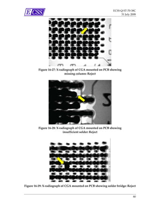
Gross defects such as missing solder ball or bridges are easily detected using
transmission X‐ray techniques. Inadequate reflow of the solder paste and open
joints are more difficult to detect, but inspecting the device from an angle can
facilitate it. This allows the operator to inspect the shape of the solder
connection as it forms onto the pad to verify that the pad is in contact with the
solder ball and that the solder is completely wetted to the pad. Inadequate
reflow of the solder paste may be seen as a jaggedness around the perimeter of
the solder balls.
For BGAs having eutectic solder balls, a tear‐drop pad design can improve the
identification of open joints or inadequate reflow [9]. If the solder paste is
properly reflowed and joined with the solder ball, the solder ball have a
distorted shape, which is easily seen in the X‐ray image. A tear‐drop pad design
can be useful also for the inspection of BGAs having high temperature balls and
for CGAs, but that has not been verified. Since the balls and columns do not
reflow for these components, the distortion of the solder joints can be expected
to be less pronounced.
Still, for thick ceramic devices, boards with a very large number of layers and
components on both side of the board, it can be impossible to inspect all solder
joints using transmission X‐ray techniques. Laminography techniques can then
be a useful tool.
X‐ray analysis is the only available non‐destructive method for the inspection
and detection of void in solder joints to area array devices. However, it is
important to use this technique with caution. Many real time X‐ray inspection
systems have an X‐ray imaging device that exhibits an aberration called
“Voltage Blooming” [5]. The result is that the size of a void is affected by the
voltage applied to the X‐ray source. If the system has this type of aberration, a
calibration is done by taking images of solder joints with voids having known
sizes.
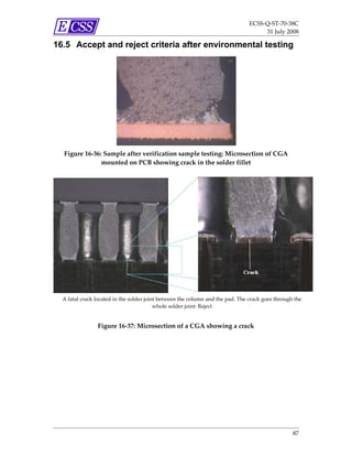
C.4.4 Microsectioning of solder joints
a. Destructive methods are used to verify the integrity of solder joints to
these devices after verification testing.
NOTE Cracks in solder joints to area array devices are
usually very difficult to detect using visual and X‐
ray inspection techniques.
b. The sample is moulded in a resin to alleviate chipping or destruction of
the sample during microsectioning.
c. The resin has an added fluorescent agent.
NOTE This facilitates the detection of fine cracks in solder
joints, but also in the PCB laminate.
107](https://image.slidesharecdn.com/ecss-q-st-70-38c-110124095254-phpapp01/85/Ecss-q-st-70-38c-107-320.jpg)
![ECSS‐Q‐ST‐70‐38C
31 July 2008
C.4.5 Dye penetrant analysis
a. Dye penetrant analysis is used as follows to analyse the integrity of the
solder joints after verification testing.
1. A low viscosity dye is applied to the sample, which penetrates any
cracks or delaminated areas.
2. The dye is dried and the device is then removed, either by prying
it away or by applying a pulling force at room temperature or
higher.
3. The presence of dye on a solder pad indicates that a crack has been
formed prior to the application of the dye. Cracks present in the
PCB laminate beneath solder pads are also be coloured with the
dye. Thus, coloured surfaces beneath solder pads that are ripped
off during the removal of the device indicate the presence of
laminate cracks after the verification testing.
NOTE For further details, see reference [5].
C.5 Verification testing
Due to the lack of stress relief on area array devices, thermo‐mechanical stresses
are more effectively transferred into the device and the PCB laminate. This can
cause cracking of conductors connecting the solder pads, of the PCB laminate
and within the device. Such cracking can be cause for rejection. Cracking of the
PCB laminate beneath solder pads improves the fatigue life of the solder joints
since it makes the joint more flexible. Therefore, it can lead to an overestimation
of the fatigue life. That is, the fatigue life can be shorter under more benign
conditions that do not cause cracking of the PCB laminate.
108](https://image.slidesharecdn.com/ecss-q-st-70-38c-110124095254-phpapp01/85/Ecss-q-st-70-38c-108-320.jpg)


![ECSS‐Q‐ST‐70‐38C
31 July 2008
Annex E (informative)
Additional information
E.1 X-Ray inspection equipment (to 6.8.7)
Various X‐ray inspection equipment is available for the non‐destructible
inspection of SMD joints that are hidden beneath packages. This includes
perpendicular transmission, angled transmission and automatic X‐ray
laminography systems.
X‐ray inspection techniques and detectable defects are described in
ESA STM‐261 [1].
E.2 Melting temperatures and choice
Table E‐1: Guide for choice of solder type
Solder type Melting range (°C) Uses
Solidus Liquidus
63 tin solder 183 183 Soldering printed circuit boards where temperature
(eutectic) limitations are critical and in applications with an
extremely short melting range. Preferred solder for surface
mount devices.
62 tin silver loaded 179 190 Soldering of terminations having silver and or silver
palladium metallization. This solder composition decreases
the scavenging of silver surfaces.
60 tin solder 183 188 Soldering electrical wire/cable harnesses or terminal
connections and for coating or pretinning metals.
96 tin silver 221 221 Can be used for special applications, such as soldering
(eutectic) terminal posts.
75 indium lead 145 162 Special solder used for low temperature soldering process
when soldering gold and gold‐plated finishes. Can be used
for cryogenic applications.
70 indium lead 165 175 For use when soldering gold and gold‐plated finishes
when impractical to degold.
50 indium lead 184 210 This solder has low gold leaching characteristic.
10 tin lead 268 290 For use in step‐soldering operations where the initial
solder joint must not be reflowed on making the second
joint (e.g. CGA columns, connections internal to devices)
115](https://image.slidesharecdn.com/ecss-q-st-70-38c-110124095254-phpapp01/85/Ecss-q-st-70-38c-115-320.jpg)
![ECSS‐Q‐ST‐70‐38C
31 July 2008
Bibliography
[1] ESA STM‐261, An Investigation into Ball Grid Array Inspection
Techniques.
[2] ESA STM‐265, Evaluation of Thermally Conductive Staking Compounds
during the Assembly of Spacecraft Electronics.
[3] ESA SP‐1173, Evaluation of Conformal Coating for Future Spacecraft
Applications.
[4] ESA STM‐266, Assessment of the Reliability of Solder Joints to Ball and
Column Array Packages for Space Applications
[5] IPC‐7095, Design and Assembly Process Implementation for BGAs, IPC,
August 2000.
[6] P.‐E. Tegehall and B. D. Dunn, Impact of Cracking Beneath Solder Pads in
Printed Board Laminate on Reliability of Solder Joints to Ceramic Ball
Grid Array Packages, ESA STM‐267, ESA Publications Division,
Noordwijk, 2003.
[7] P.‐E. Tegehall And B.D Dunn, Assessment of the Reliability of Solder
Joints to Ball And Column Grid Array Packages for Space Applications,
ESA STM‐266, ESA Publications Divisions, Noordwijk, 2003.
[8] P. Wood and H. Rupprecht, BGA and CSP Rework: What is involved? K.
Gilleo (Ed.) Area Array Packaging Handbook, McGraw‐Hill, Inc., 2001,
Chapter 19.
[9] M. Wickham, C. Hunt, D.M. Adams and B.D. Dunn, An Investigation into
Ball Grid Array Inspection Techniques, ESA STM‐261, ESA Publications
Divisions, Noordwijk, 1999.
[10] ECSS‐E‐ST‐10‐03, Space engineering — Testing.
[11] ECSS‐Q‐ST‐70‐22, Space product assurance — Control of limited shelf‐
life materials.
[12] ECSS‐Q‐ST‐70‐28, Space product assurance — Repair and modification
of printed circuit board assemblies for space use.
[13] ISO 9453, Soft solder alloys ‐ Chemical compositions and forms
116](https://image.slidesharecdn.com/ecss-q-st-70-38c-110124095254-phpapp01/85/Ecss-q-st-70-38c-116-320.jpg)


