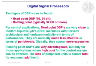
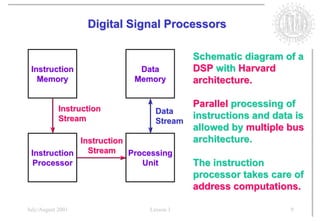
The document provides information on digital control applications using digital signal processors (DSPs) and microcontrollers (μCs) in power electronics. It discusses the advantages and disadvantages of digital control, available tools for implementation including DSPs and μCs, and features of DSPs and new DSP solutions that combine DSP capabilities with peripheral units typically found in μCs. Specific DSP solutions - the Analog Devices ADMC401 and Texas Instruments TMS320F240 - are described in detail including their core features, peripheral units, and software examples.


![Digital Signal Processors [1]
First development in the late 70’s (TMS320C10 - 1979).
Typically designed for open loop digital signal
processing e.g.:
• real time FFT calculation;
• digital filtering of sampled signals.
The market for this kind of applications is enormous
and steadily growing, including telecom and consumer
electronics.
Applications in industrial electronics (control tasks) are
rather insignificant in volume. The manifacturers offer
very few control oriented solutions.
July/August 2001 Lesson 1 7](https://image.slidesharecdn.com/lesson1-130128185005-phpapp01/85/dsp-Lesson1-7-320.jpg)
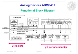
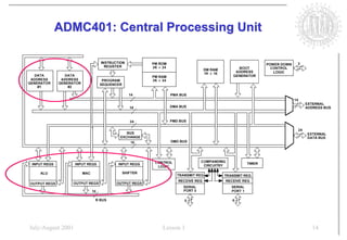
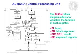
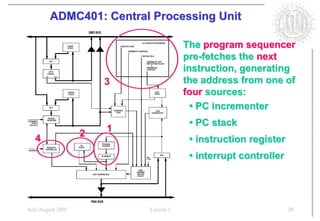
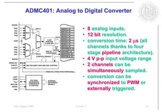
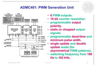
![Analog Devices ADMC401 [2]
• Fixed-point DSP core features:
♦ 26 MIPS performance;
♦ ADSP 21xx compatible;
♦ Single cycle instruction execution
(38.5 ns @ 13 MHz clock frequency);
♦ 16 bit arithmetic and logic unit;
♦ Single Cycle 16 bit X 16 bit MAC.
• Built-in peripheral units:
♦ High resolution multi-channel ADC;
♦ Three-phase 16 bit PWM generation unit;
♦ dual channel event timer unit (CAPCOM);
♦ Incremental encoder interface unit.
July/August 2001 Lesson 1 12](https://image.slidesharecdn.com/lesson1-130128185005-phpapp01/85/dsp-Lesson1-12-320.jpg)
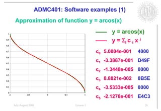
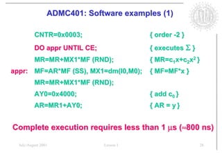
![ADMC401: Software examples (1)
.VAR/DM/RAM/SEG=USER_DM3 ACOS_COEFF[5];
.INIT ACOS_COEFF: 0xD49F, 0x0000, 0x0B5E, 0x0000, 0xE4C3;
Arcos:
AR=-AR; { invert sign x=-x }
;
M0=1; L0=0;
I0=^ACOS_COEFF; { pointer to coefficient vector }
;
MY1=AR; { writes AR to MY1. Now MY1 = x}
;
MF=AR*MY1 (SS), MX1=dm(I0,M0); {MF = x2}
MR=MX1*MY1 (RND), MX1=dm(I0,M0); {MR = c1x}
July/August 2001 Lesson 1
parallel instructions
27](https://image.slidesharecdn.com/lesson1-130128185005-phpapp01/85/dsp-Lesson1-27-320.jpg)
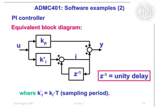
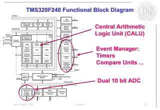
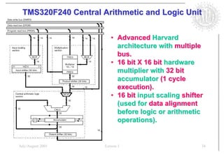
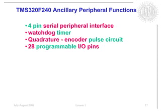
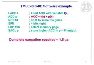
![Texas Instruments TMS320F240 [3]
• Fixed-point DSP core features:
♦ 20 MIPS performance;
♦ TMS320C25 source code compatible;
♦ Single cycle instruction execution
(50 ns @ 20 MHz CPU clock frequency);
♦ 16 bit arithmetic and logic unit;
♦ Single Cycle 16 bit X 16 bit signed product.
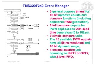
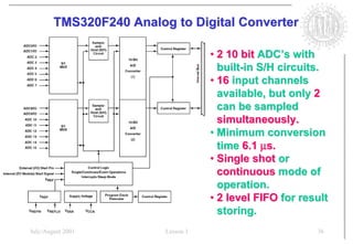
• Main built-in peripheral units:
♦ 10 bit resolution, 16 channel ADC;
♦ 12 channel 16 bit PWM generation unit;
♦ 3 16 bit general purpose timers;
♦ 4 independent capture circuits.
July/August 2001 Lesson 1 32](https://image.slidesharecdn.com/lesson1-130128185005-phpapp01/85/dsp-Lesson1-32-320.jpg)
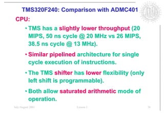
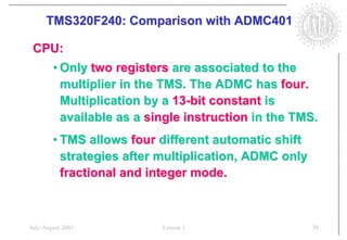
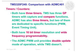
![TMS320F240: Comparison with ADMC401
Timers / Counters:
• TMS offers an embedded SVM hardware
module to automatically implement a flat-top
type of PWM modulation. This simplifies the
software [4] to some extent (T1 and T2 have
to be computed).
July/August 2001 Lesson 1 41](https://image.slidesharecdn.com/lesson1-130128185005-phpapp01/85/dsp-Lesson1-41-320.jpg)
![References
[1] P. Pirsch, “Architectures for Digital Signal Processing”, 1998,
John Wiley and Sons (ISBN 0-471-97145-6).
[2] Analog Devices Winter 1999 Designers’ Reference Manual.
[3] Texas Instruments 1999 TMS320 DSP Solutions CD-ROM.
[4] Texas Instruments, Application Report SPRA524, ”Space-Vector
PWM With TMS320C24x/F24x Using Hardware and Software
Determined Switching Patterns”.
July/August 2001 Lesson 1 47](https://image.slidesharecdn.com/lesson1-130128185005-phpapp01/85/dsp-Lesson1-47-320.jpg)