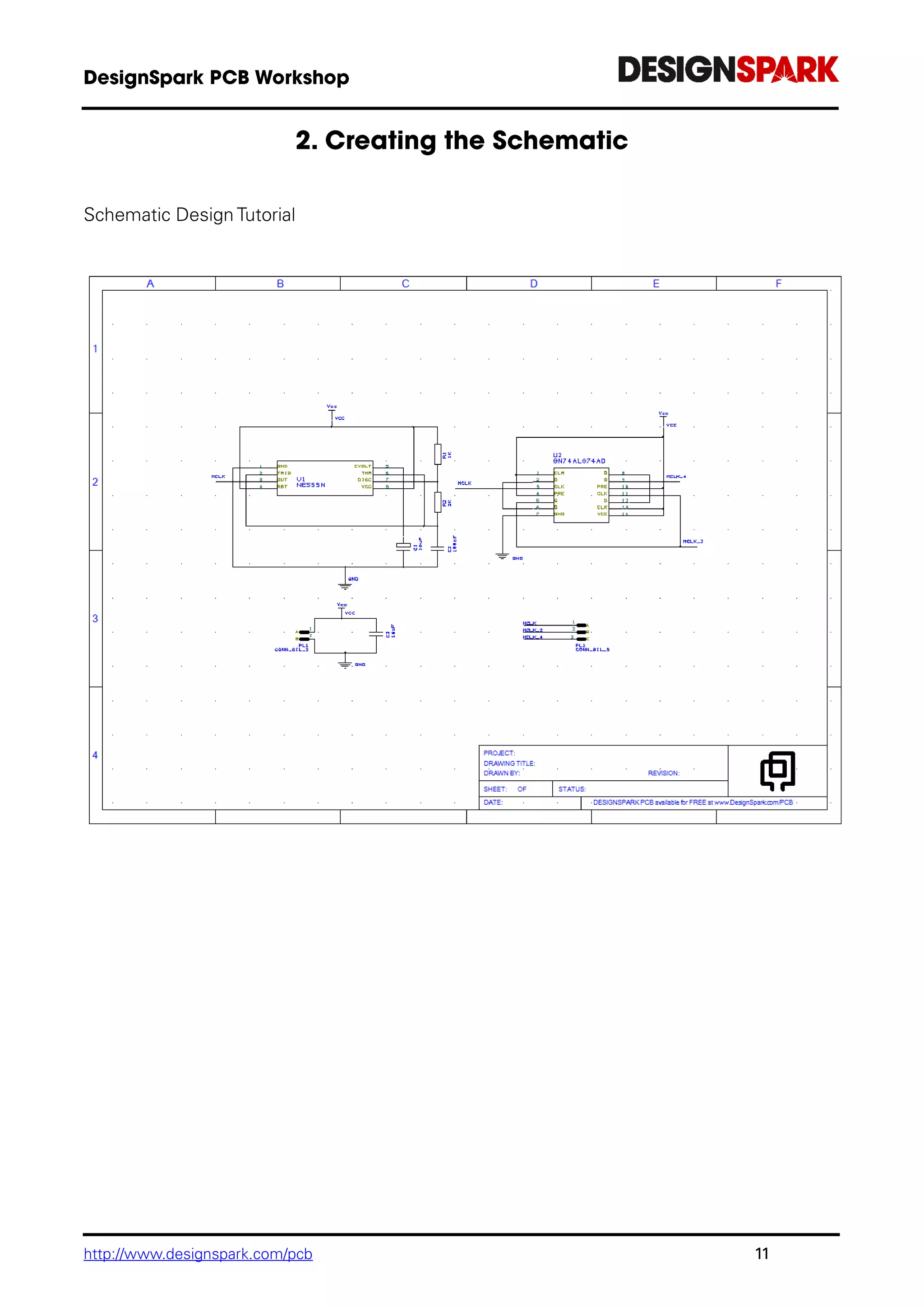
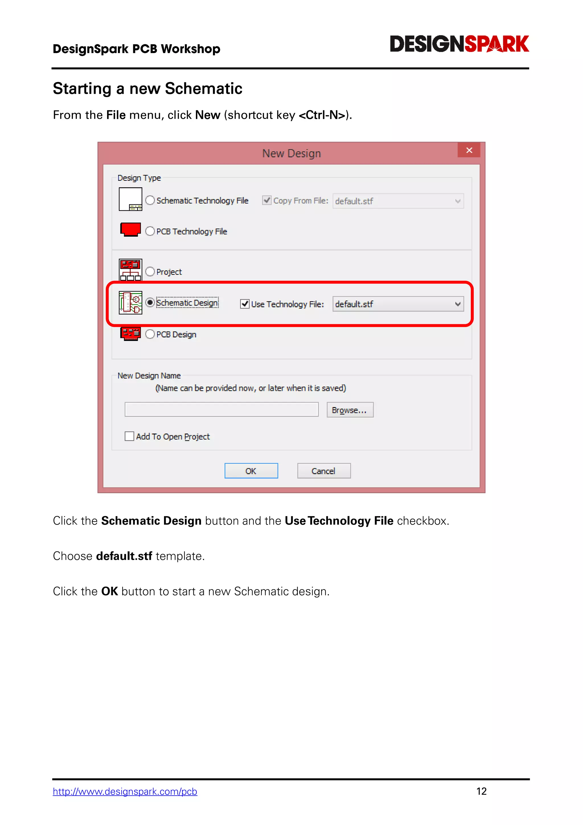
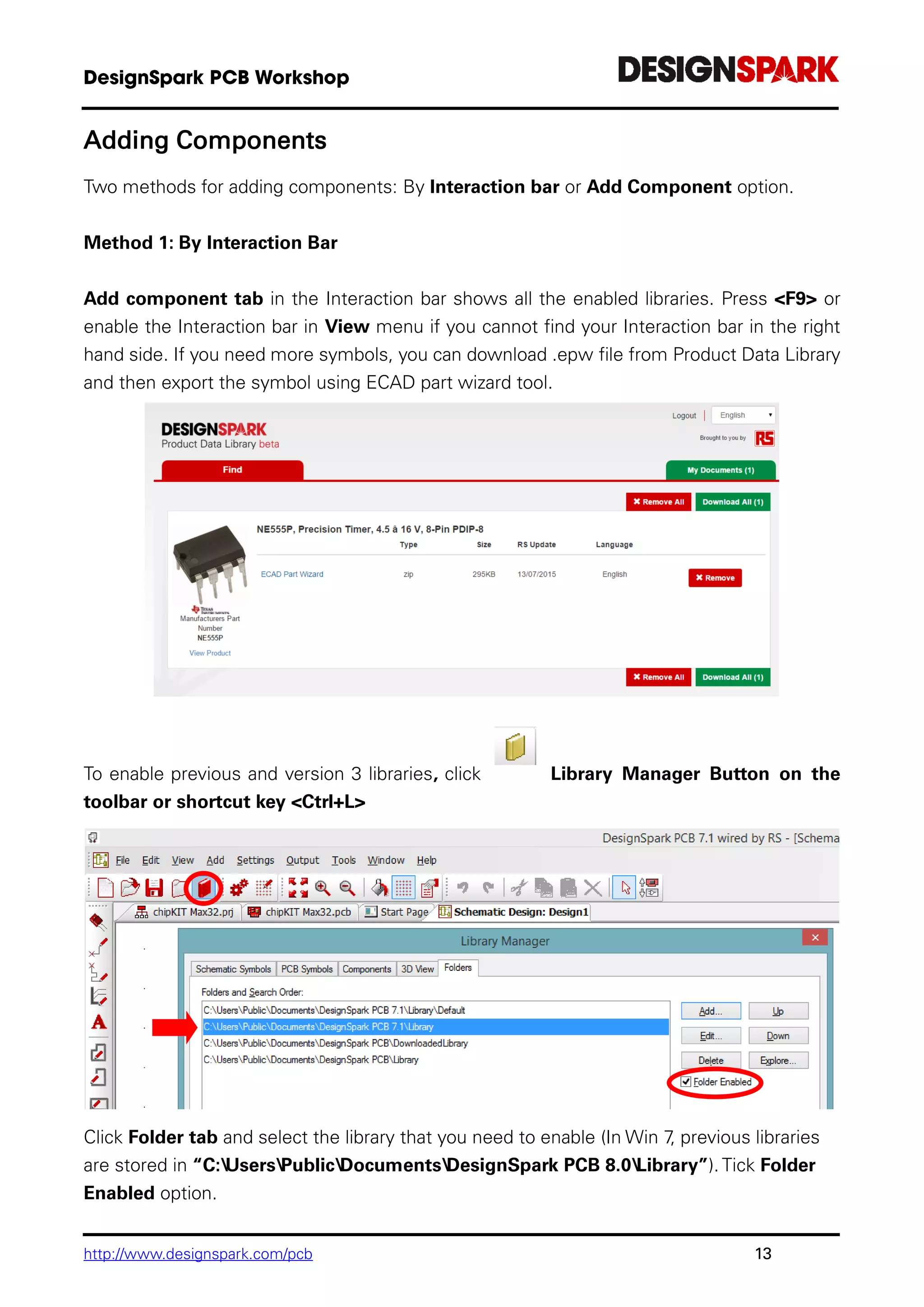
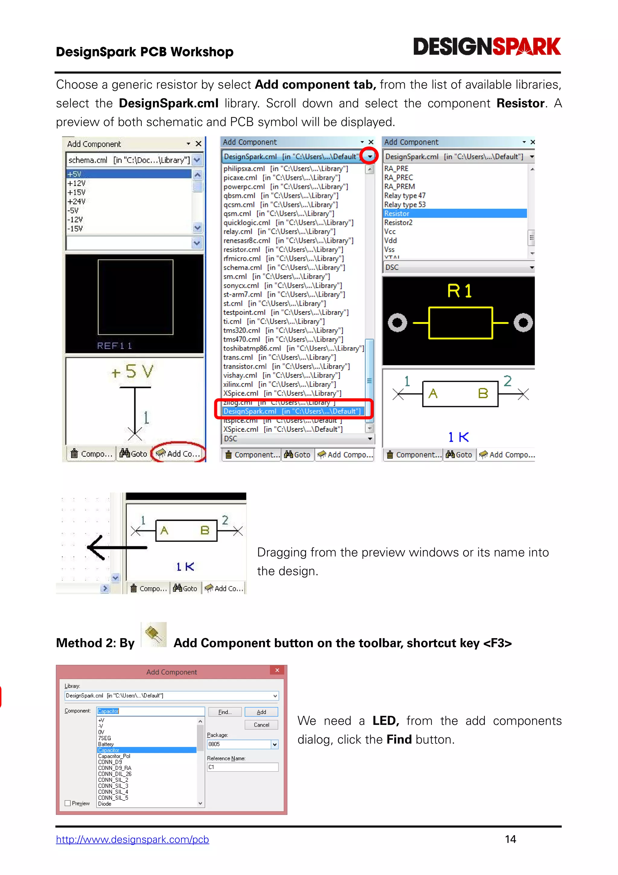
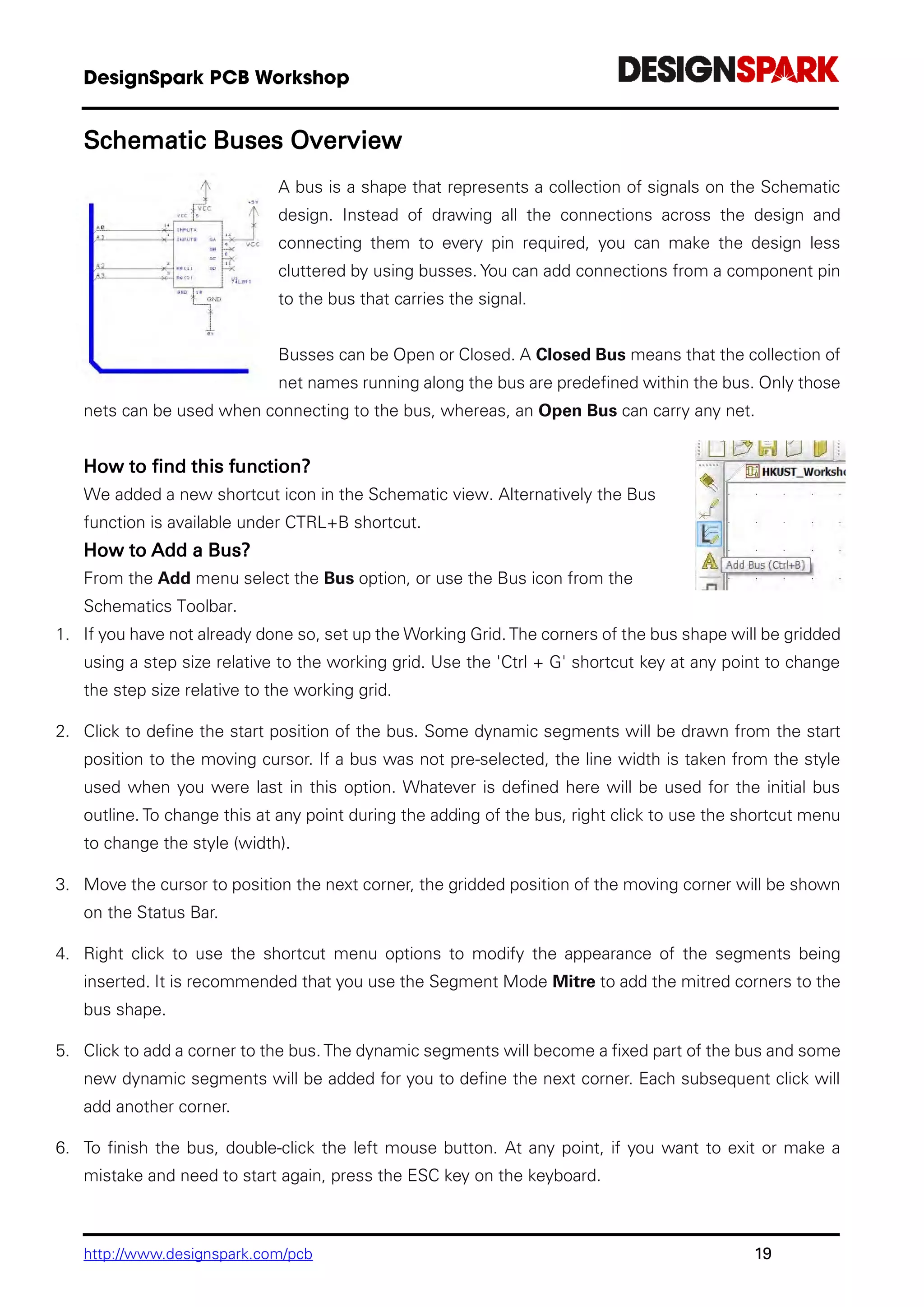
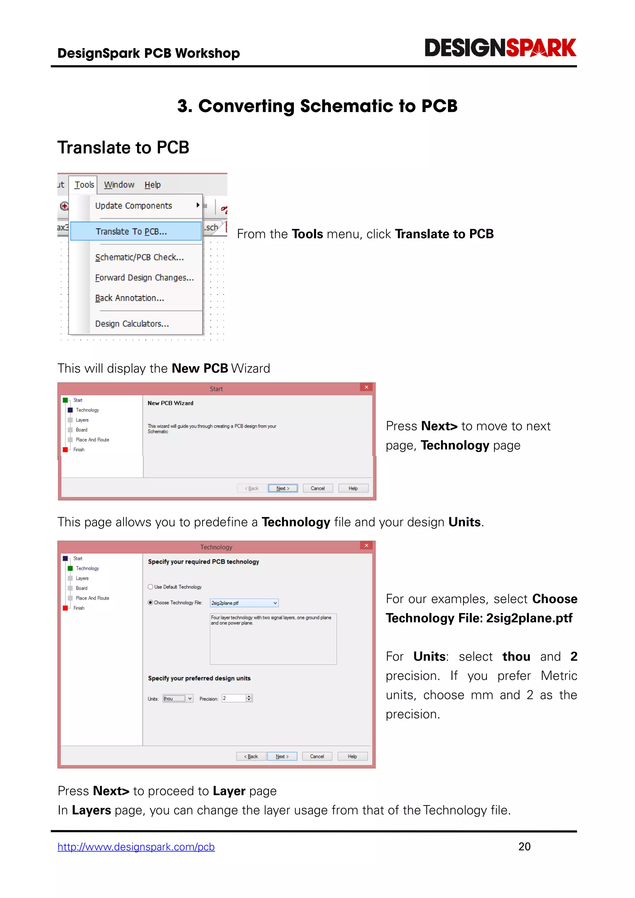
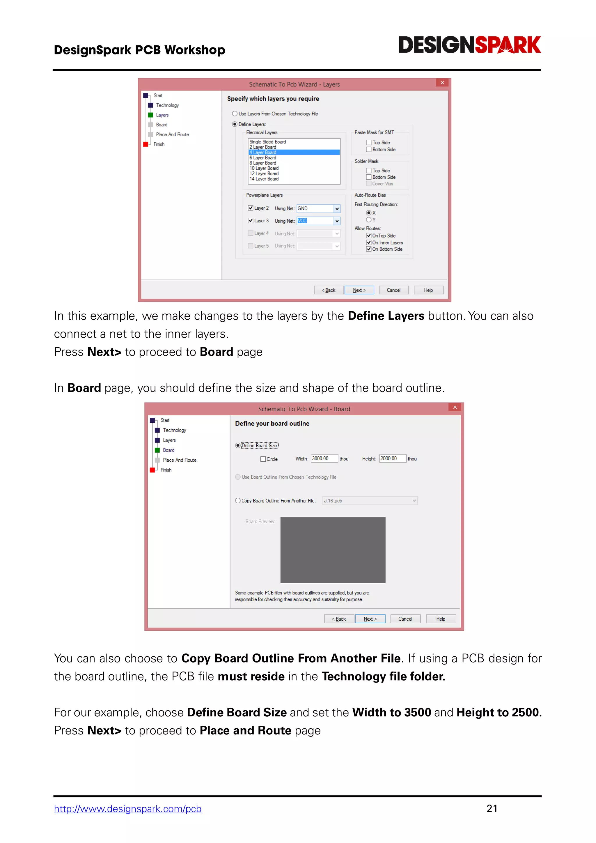
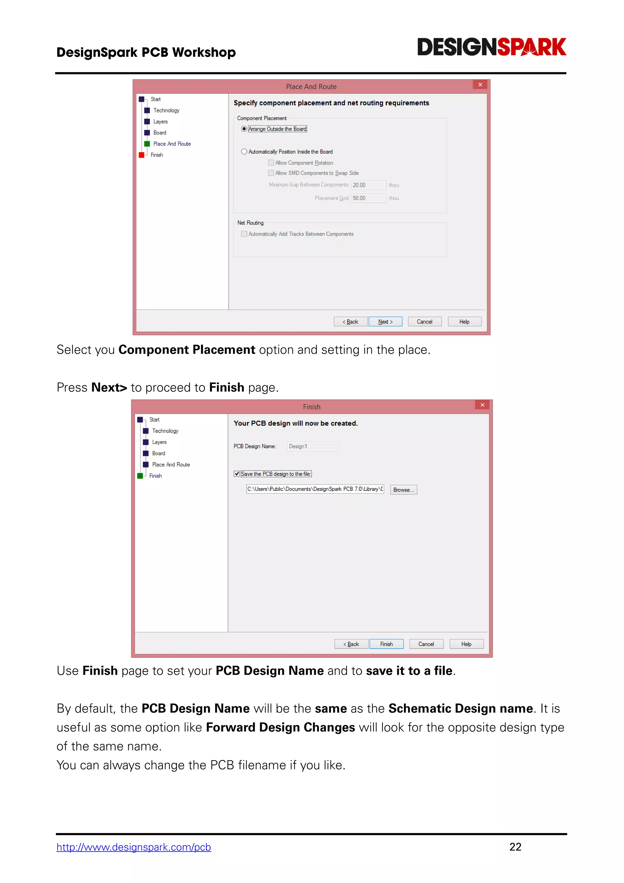
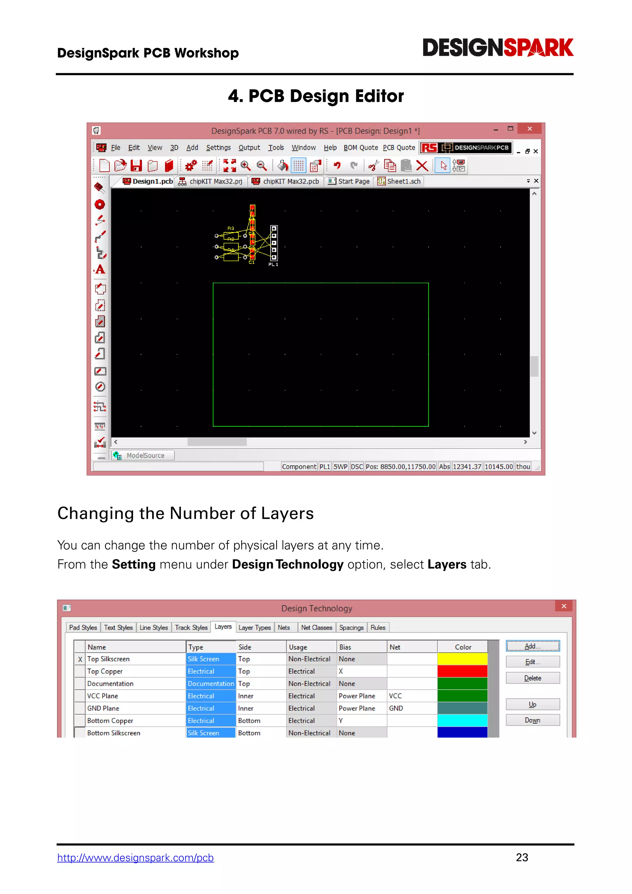
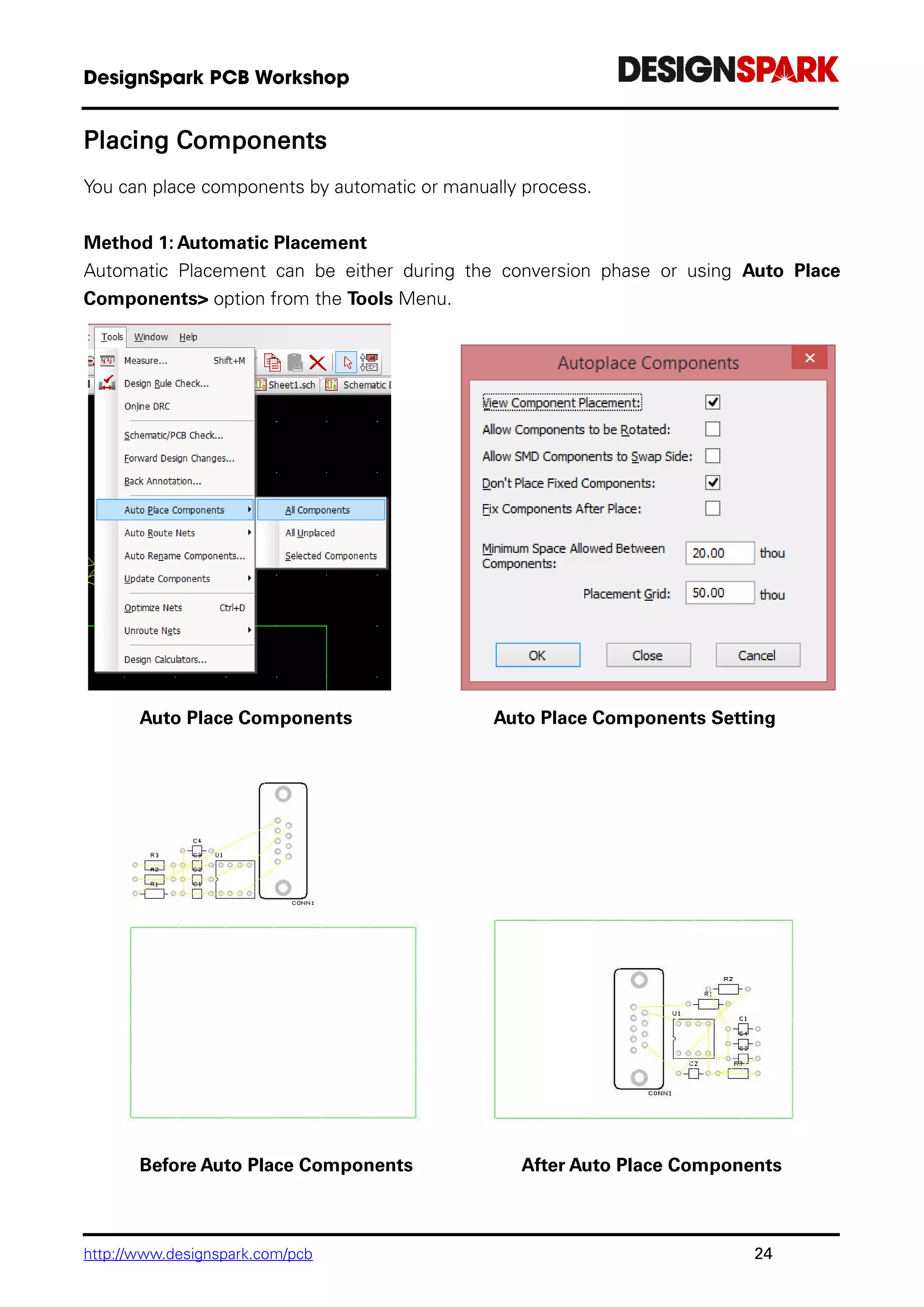
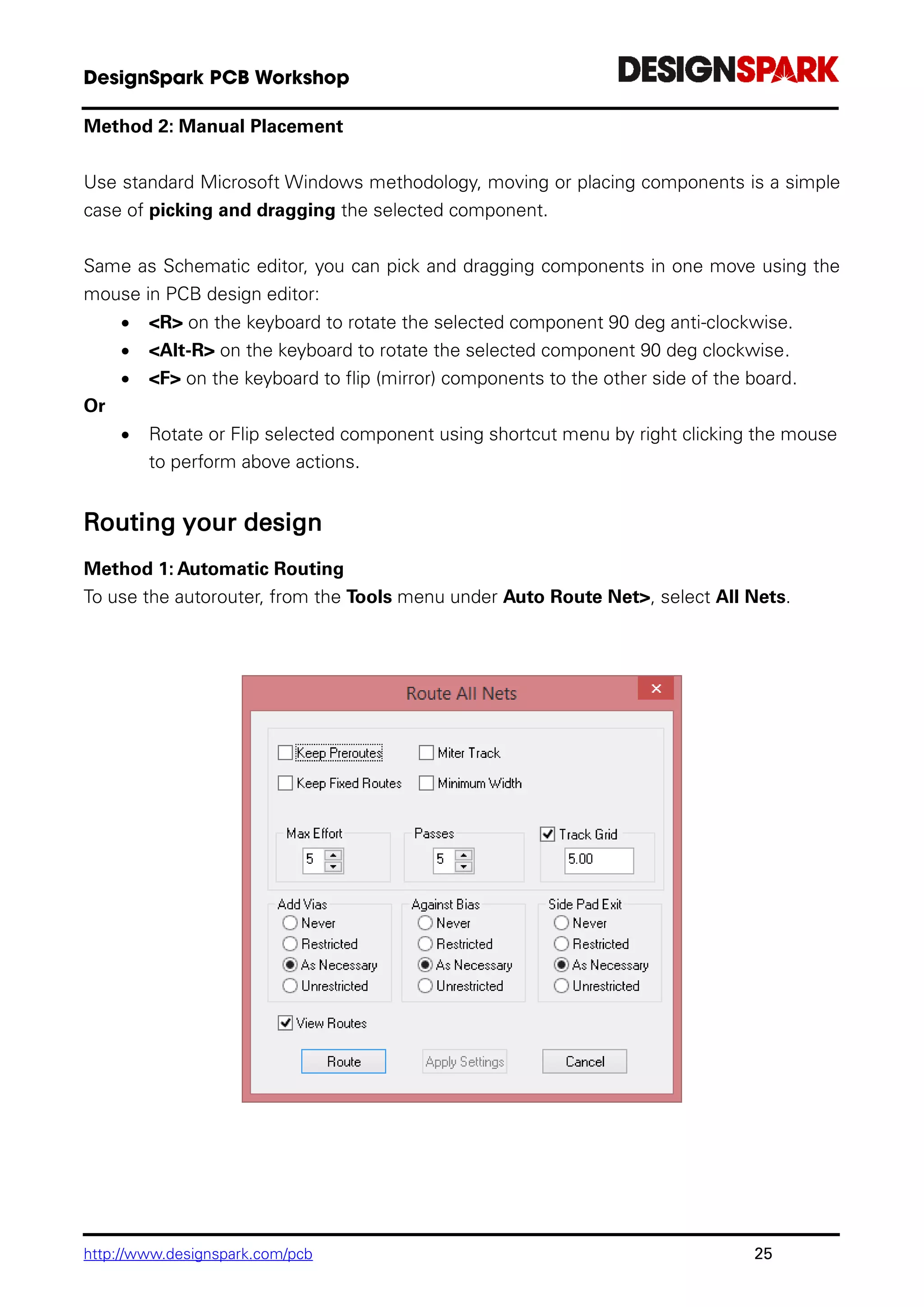
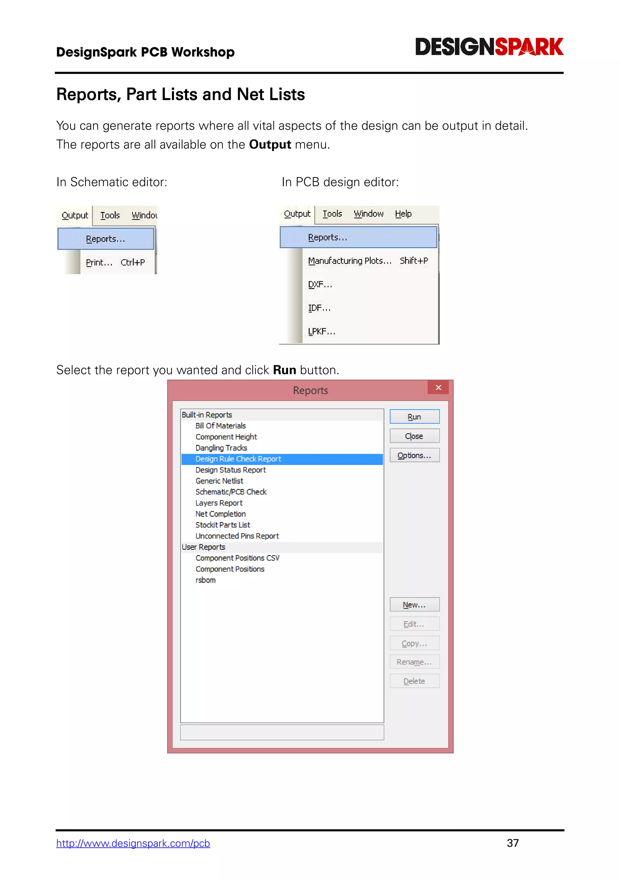
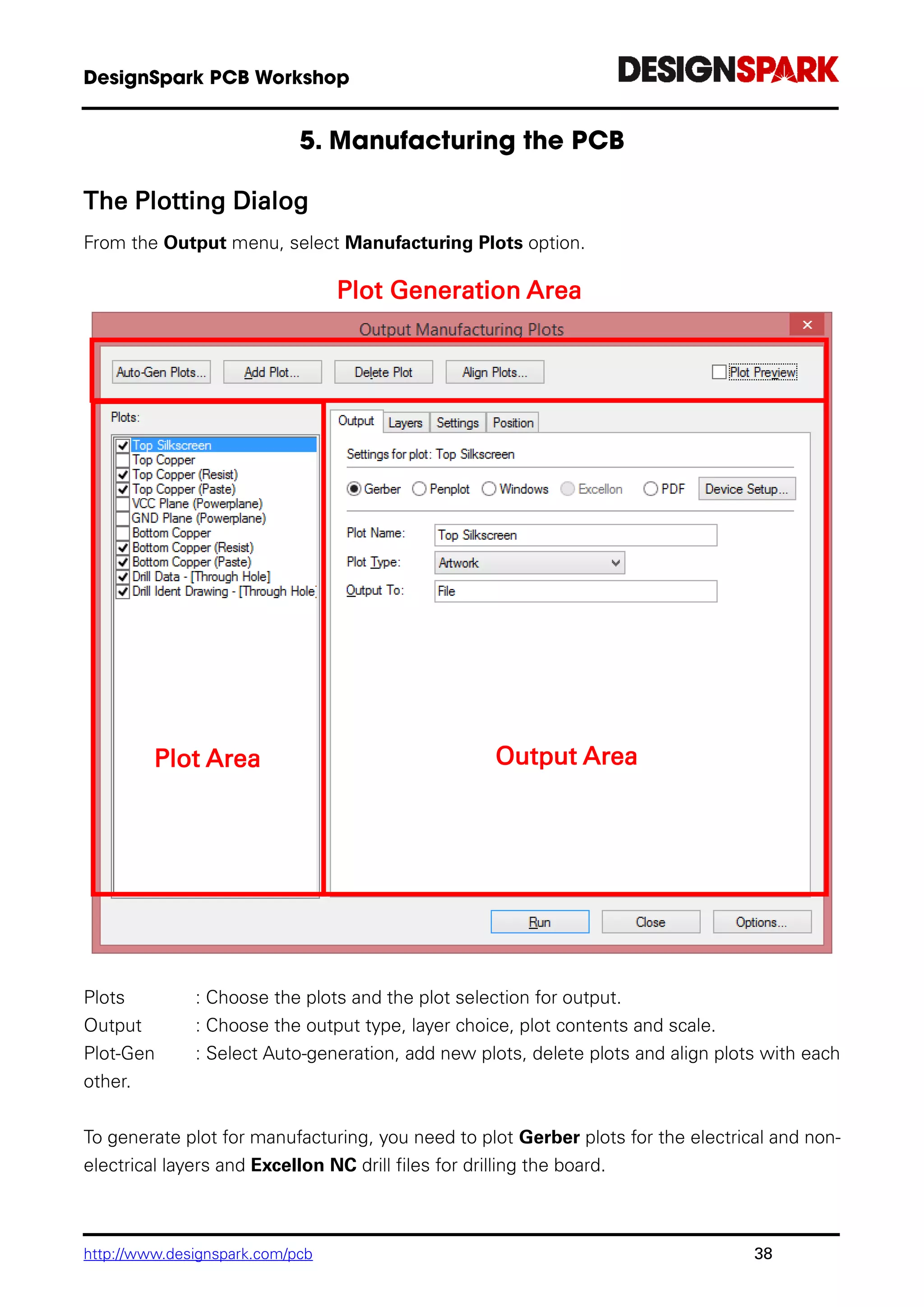
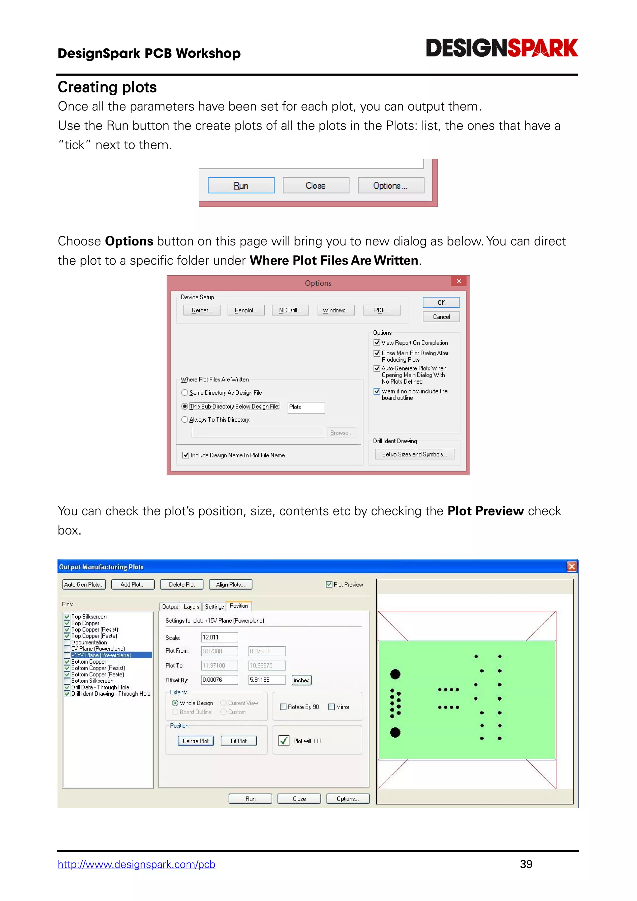
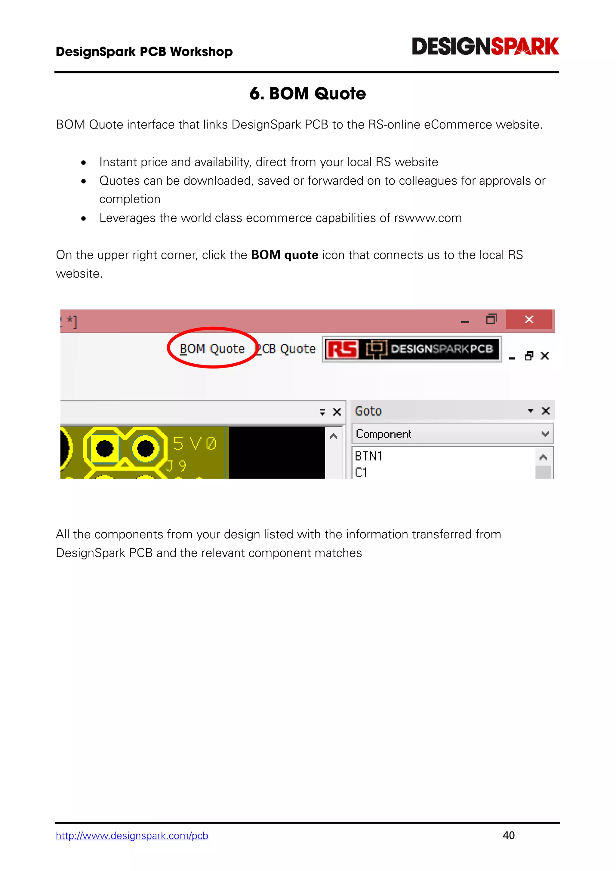
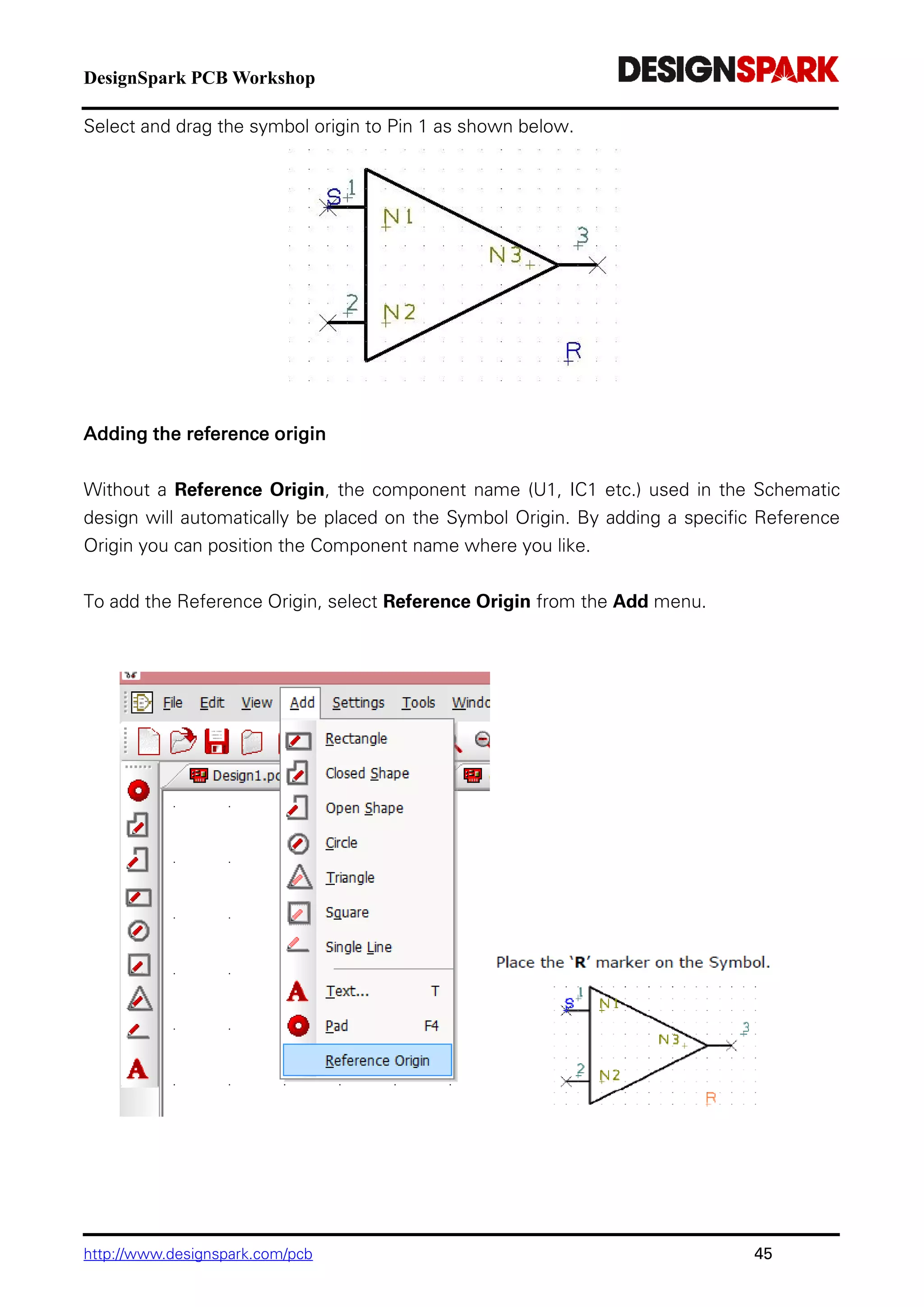
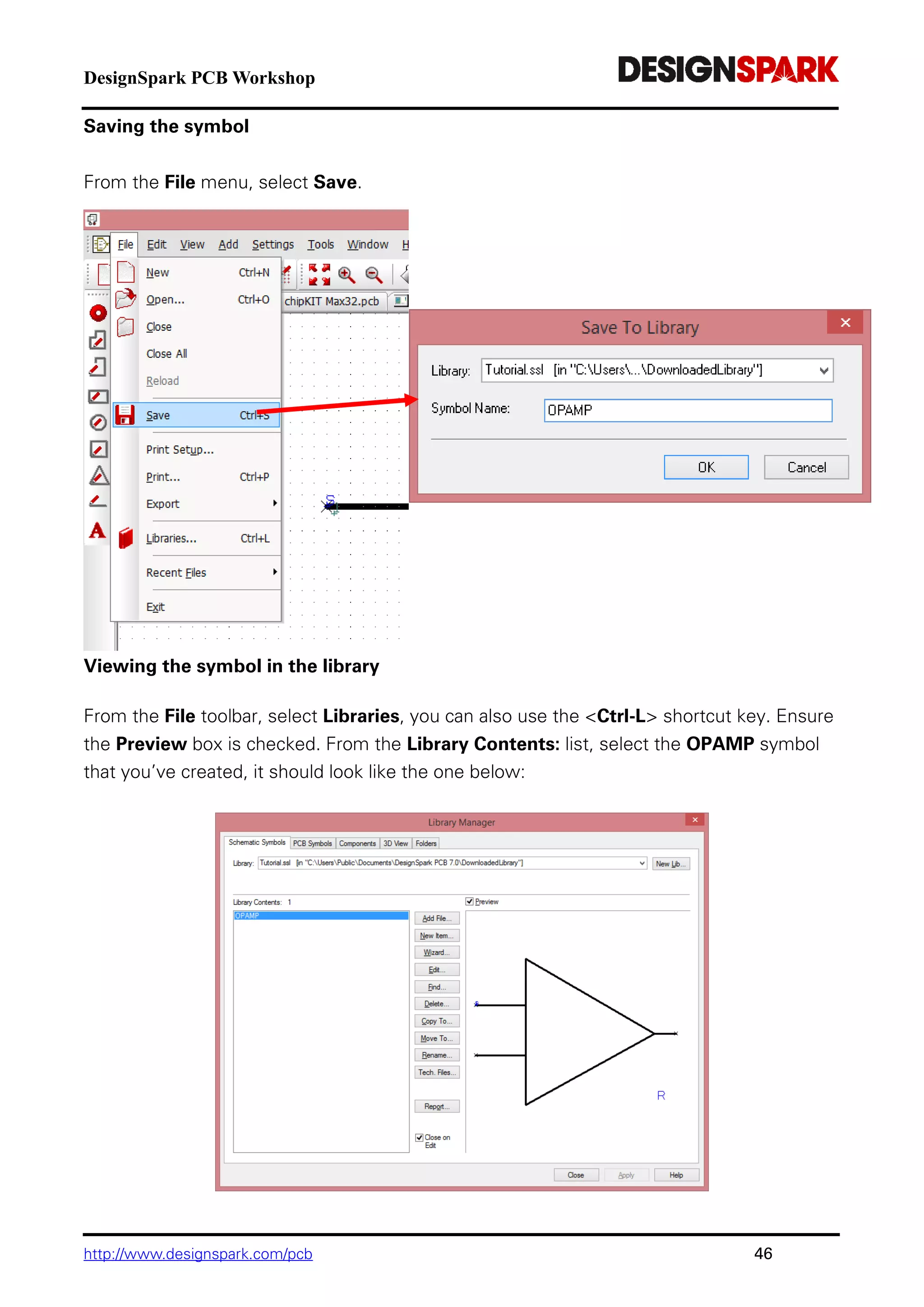
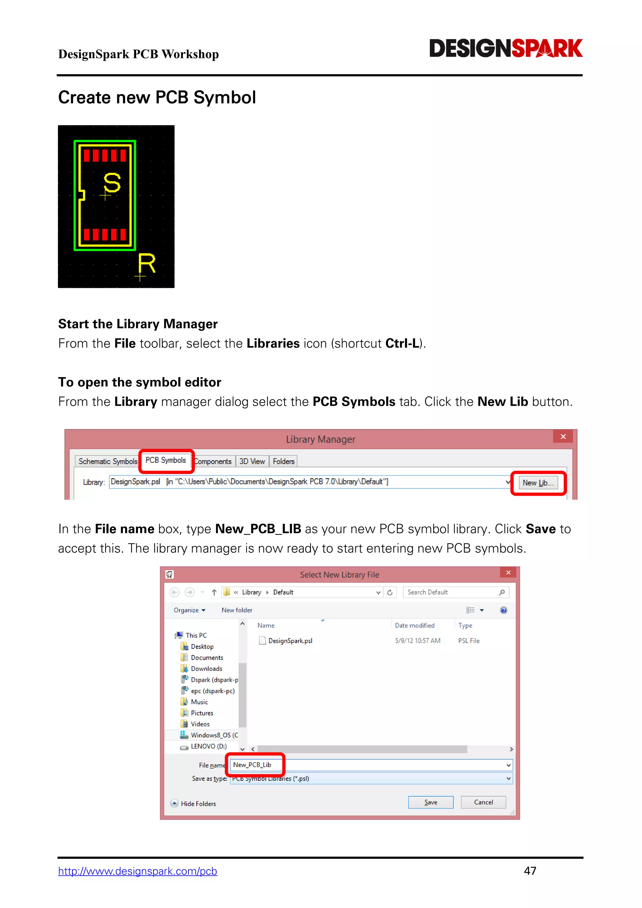
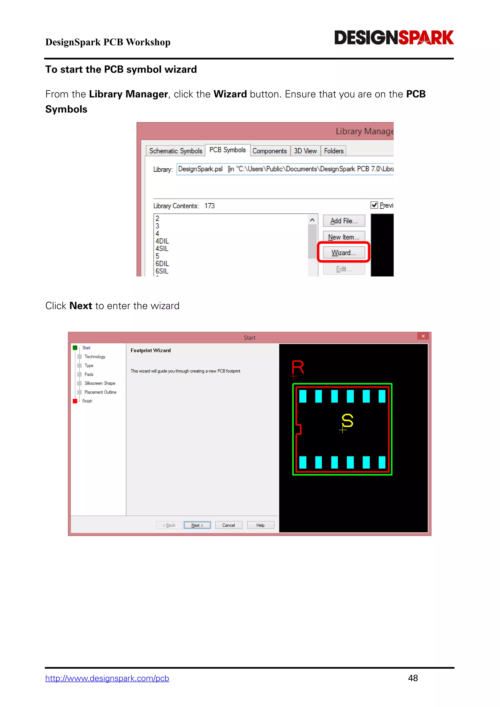
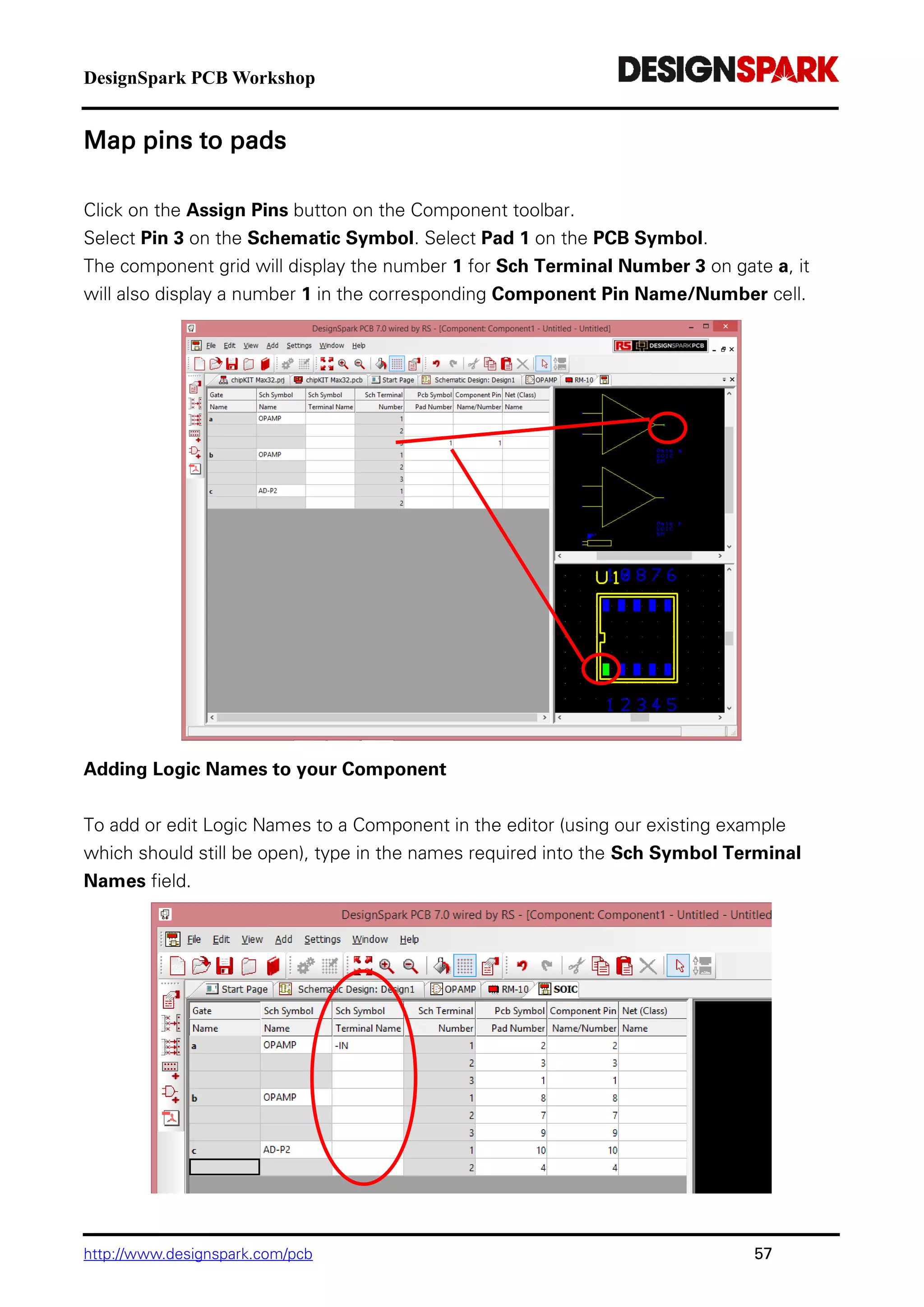
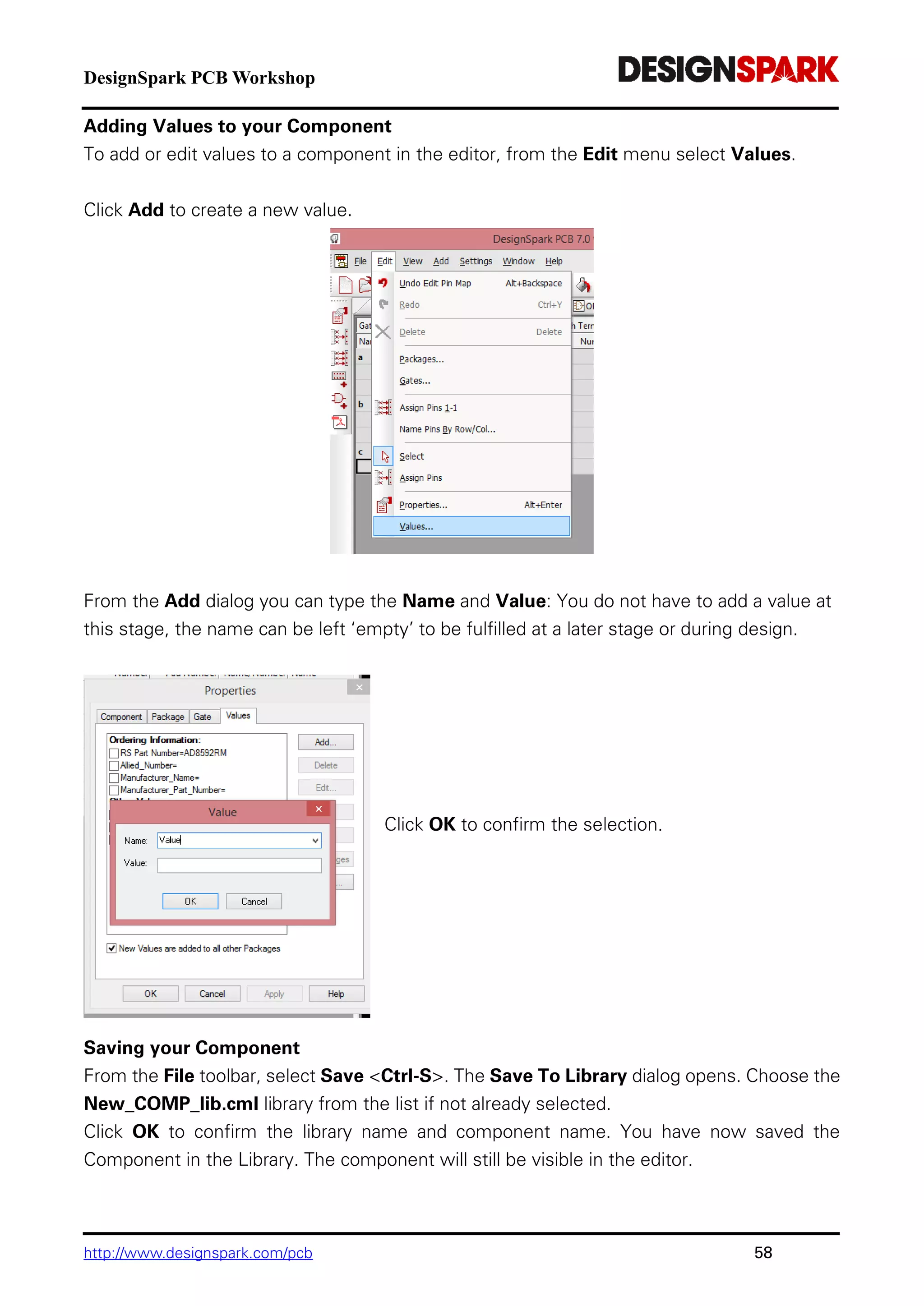
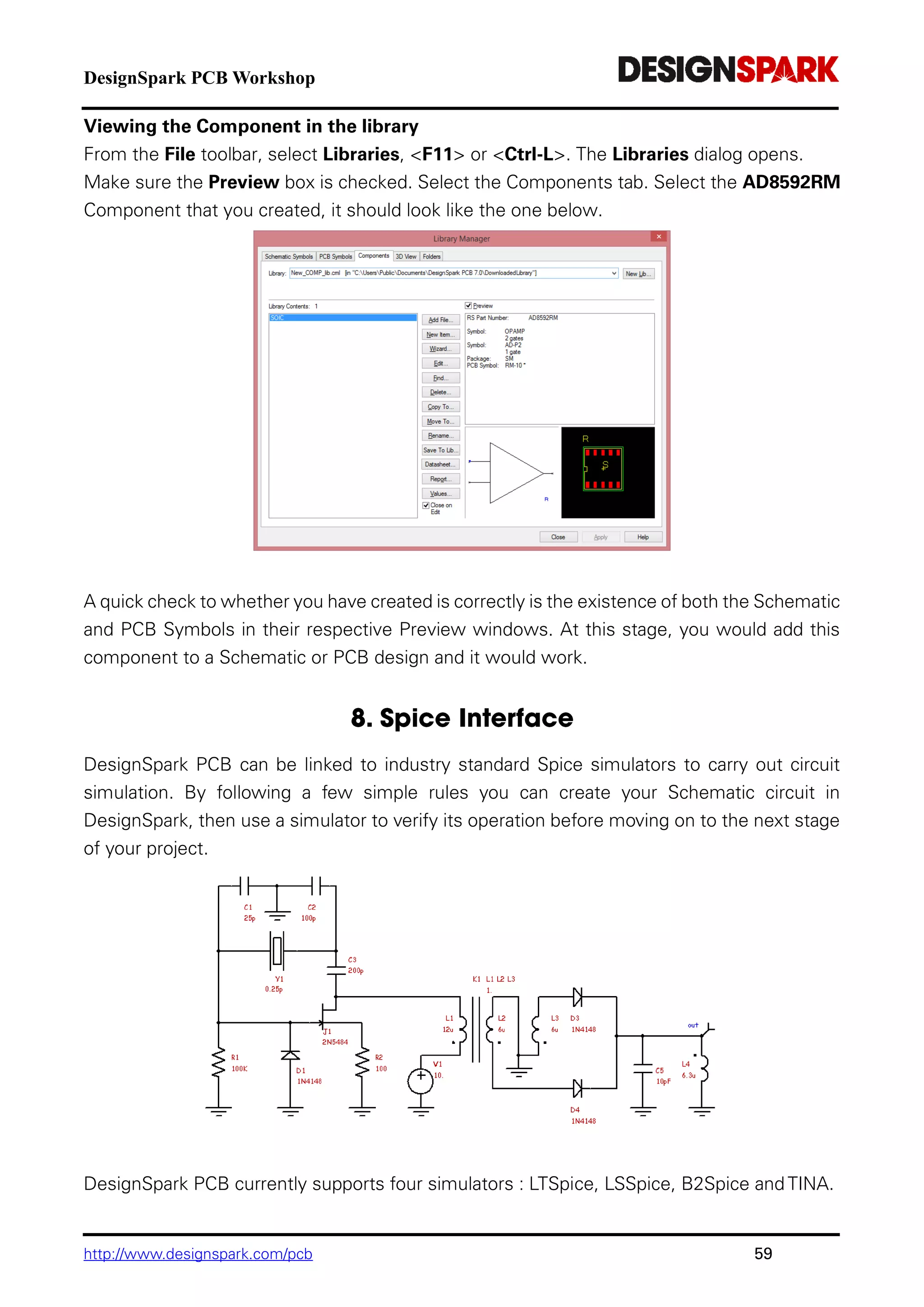
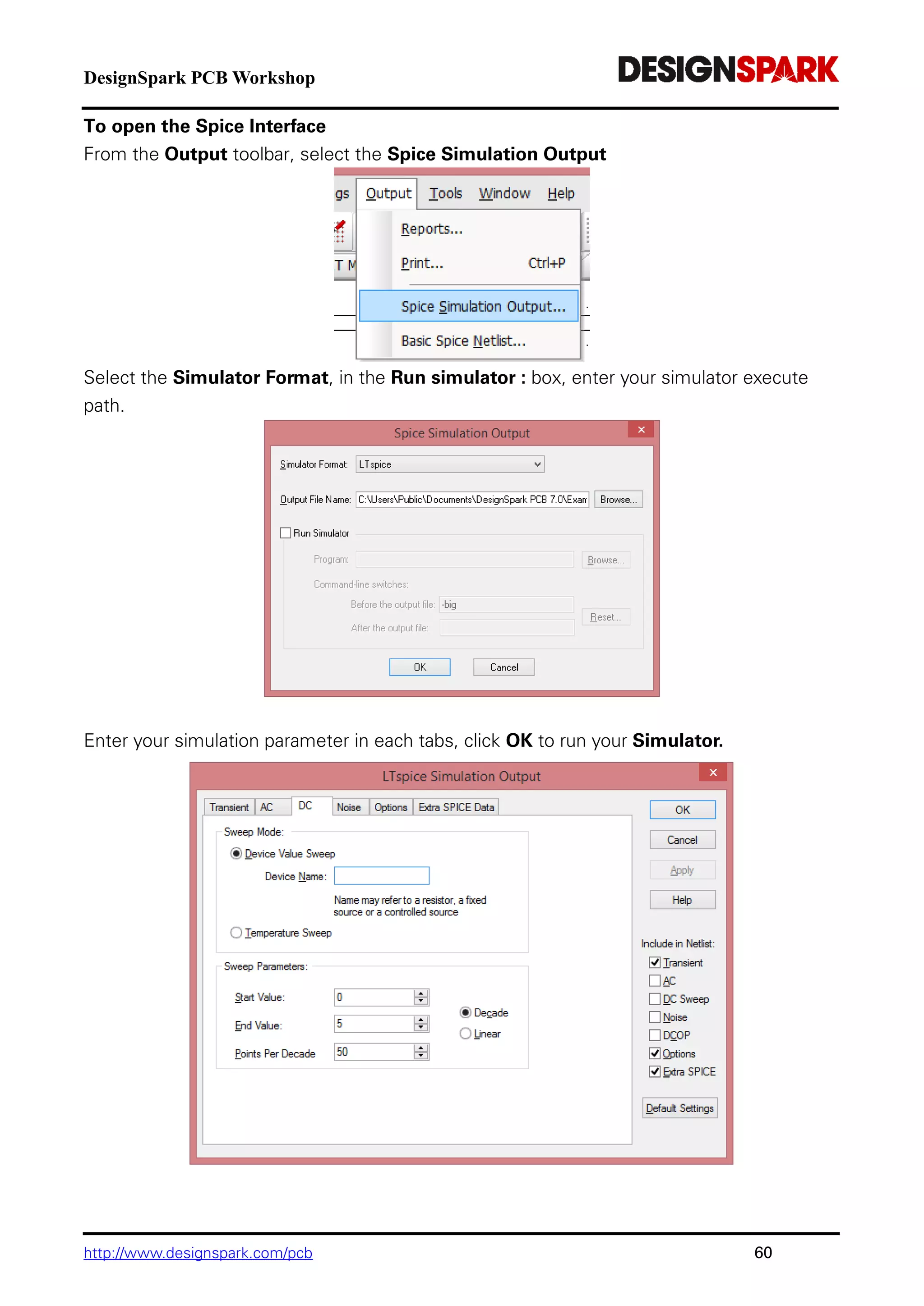
Step by step guide to teach you how to use free DesignSpark PCB software to design from schematic diagram to PCB layout and generate manufacturing output.
Gestione degli eventi indesiderati, compiti del RSPPCorrado Cigaina
infortuni, quasi infortuni, malattie professionali e danni materiali, devono essere analizzati e registrati in modo tale da evitare che simili eventi possano ripetersi. RSPP deve assistere il datore di lavoro in questo importante compito.
InduSoft Web Studio v7.1 + SP3 Best PracticesAVEVA
System integrators are tasked with meeting strict requirements for projects, and may need to develop value-added functionality for their solutions. HMI software platforms like InduSoft Web Studio can provide the framework for customer solutions, and InduSoft has made it a priority to support system integrators who use InduSoft Web Studio. Join us for a webinar in which we discuss best practices for system integrators. We will be offering advice for developing projects and efficiently, and share some of the benefits of the InduSoft Certified System Integrator program.
A- LES CONCEPTS
Comprehension du bim.
Travailler dans différentes vues.
Classement et hierarchie des éléments dans Revit.
B-L'ENVIRONNEMENT DE TRAVAIL
Page des fichiers rescents et grand R.
Le ruban.
Fenêtre des propriétés.
Explorateur du projet.
Navigation dans un modèle.(zoom, rotation et panoramique).
Selection des objets, et verouillage.
C-DEMARRAGE D'UN PROJET.
Les gabarits.
Travail collaboratif.
Configuration d'un nouveau projet.
Manipulation des niveaux.
Manipulation des files de projet.
Utilisation des cotes temporaires.
C- MODELISATION PAR OBJETS:
Ajout des murs.
Propriété et type de murs.
Utilisation des accroches.
Ajouts de poteaux et poutres.
Ajout de portes et fenêtres.
Ajout d'élements de plomberie et d'électricité.
Utilisation de la jonction entre murs.
Utilisation des contraintes.
D- LIENS, IMPORTS ET GROUPES:
Lier fichiers DWG/DXF/SKP
Création de topogrpahie d'un site à partir d'un fichier.
Création et gestion des groupes.
Création et gestion des liens Revit.
Utilisation du partage d'emplacement.
E- MODELISATION PAR ESQUISSE:
Sols., toits et plafonds.
Toit par extrusion.
Ouvertures.
F-ESCALIERS.
Edition avancée d'escalier.
Edition avancée de gardes corps.
G- EDITION AVANCEE DES MURS:
Création d'un nouveau type de murs..
Création et gestion des murs empilés.
Création et gestion des murs rideaux.
.
H- GESTION DES GRAPHISMES:
Gestion du style des objets.
Gestion du remplacement de la visibilité et du graphisme des éléments.
Création et application des gabarits de vue.
Cacher et isoler les éléments.
Cadrage de la vue.
Plage de vue et entendues.
Vue isométrique d'une selection.
Option d'affichage des graphismes.
I- PIECES:
Création et gestion des pièces.
J- NOMENCLATURE ET ETIQUETTES:
Gestion des étiquettes.
Création et gestion des nomenclatures.
Modification des nomenclatures.
Enrichissement des VCCTP par les nomenclatures.
K-ANNOTATIONS.
Textes.
Dimensions
Symboles.
Légendes.
Détails.
Définir ses annotations.
L- PARAMETRIQUE ET FAMILLES
Utilisation des paramètres en mode projet.
Concept de famille.
Création d'une famille.
Utilisation des contraintes.
Utilisation des formes solides.
M- FEUILLE, IMPRESSION, PUBLICATION:
Création d'une feuille d'impression.
Export CAO.
Publication.
Impression PDF.
N- TRUCS ET ASTUCES.
A découvrir en formation.
http://structalis.fr
EELE 5331 Digital ASIC DesignLab ManualDr. Yushi Zhou.docxtoltonkendal
EELE 5331: Digital ASIC Design
Lab Manual
Dr. Yushi Zhou
Department of Electrical Engineering
Lakehead University
Thunder Bay, Ontario, Canada
Contents
1 Introduction . . . . . . . . . . . . . . . . . . . . . . . . . . . . 2
2 MOSFET Devices and Layout Tutorial . . . . . . . . . . . . . 4
2.1 Prepare For Schematic . . . . . . . . . . . . . . . . . . 4
2.2 Perform Simulation . . . . . . . . . . . . . . . . . . . . 7
2.3 Layout . . . . . . . . . . . . . . . . . . . . . . . . . . . 11
2.4 Layout Veri�cation . . . . . . . . . . . . . . . . . . . . 17
2.5 Report . . . . . . . . . . . . . . . . . . . . . . . . . . . 25
2.6 How to understand DRC error report . . . . . . . . . . 26
3 CMOS Inverter . . . . . . . . . . . . . . . . . . . . . . . . . . 27
3.1 Design speci�cations . . . . . . . . . . . . . . . . . . . 27
3.2 Lab Procedure . . . . . . . . . . . . . . . . . . . . . . 29
3.3 Report . . . . . . . . . . . . . . . . . . . . . . . . . . . 31
1
EELE5331:Digital ASIC Design [email protected]
1 Introduction
This lab manual is an essential components of EELE5331: Digital ASIC
Design, o�ered by Dr. Yushi Zhou. The lab works consists of schematic
entry, symbol generation, pre-layout simulation, layout, physical and logic
veri�cation, extraction and post-layout simulation for the design. All the
students are required to submit individual lab report before the deadline.
All reports must be typed and professionally prepared. The content that
needs to be included in the report are given at the end of each lab. There
are total three labs, and each part will be released before the lab starts.
• Lab 1: MOSFET devices and layout tutorial
• Lab 2: CMOS Inverter
• Lab 3: CMOS Digital Logic Circuits
It should be noted that the students are not limited to the assigned lab
time, which may not be enough to complete the lab. Students are expected
to work on the lab during their free time if that case is required. You may
use remote log-in to complete the labs.
TSMC CMOS 180 nm technology process design kit (PDK) is a 1-Poly,
6-Metal technology, with a maximum supply voltage of 1.8 V for thin oxide
devices and 3.3 V for thick oxide devices. This process is suitable for design-
ing analog, digital, RF and mixed-signal circuits and systems. In this course,
all the labs are designed based upon CMOS 180 nm process. The computer-
aided design (CAD) tools that are adopted in this course are from Cadence
Design Systems for the purpose of schematic entry, simulation, implemen-
tation and veri�cation. The Cadence custom IC design platform provides
a graphical interface for various stages in the design �ow. An overview of
the design �ow and which tools are involved in each stage is shown in Fig.1.
As you may notice that there are loops, indicating iterative procedures. For
instance, if the physical layout does not pass design rules check or LVS check,
Page 2
EELE5331:Digital ASIC Design [email protected]
the modi�cation of.
Creating first project in mikroC PRO for 8051inovabrasil
Fonte: http://www.mikroe.com/downloads/get/304/1st_project_8051_c_v100.pdf [27/03/2014]
Programação de microcontroladores 8051 (MCS-51) em linguagem C.
Para baixar a versão demo do programa compilador mikroC PRO for 8051 [site da MikroElektronika]:
http://www.mikroe.com/mikroc/8051/overview/
Water scarcity is the lack of fresh water resources to meet the standard water demand. There are two type of water scarcity. One is physical. The other is economic water scarcity.
A- LES CONCEPTS
Comprehension du bim.
Travailler dans différentes vues.
Classement et hierarchie des éléments dans Revit.
B-L'ENVIRONNEMENT DE TRAVAIL
Page des fichiers rescents et grand R.
Le ruban.
Fenêtre des propriétés.
Explorateur du projet.
Navigation dans un modèle.(zoom, rotation et panoramique).
Selection des objets, et verouillage.
C-DEMARRAGE D'UN PROJET.
Les gabarits.
Travail collaboratif.
Configuration d'un nouveau projet.
Manipulation des niveaux.
Manipulation des files de projet.
Utilisation des cotes temporaires.
C- MODELISATION PAR OBJETS:
Ajout des murs.
Propriété et type de murs.
Utilisation des accroches.
Ajouts de poteaux et poutres.
Ajout de portes et fenêtres.
Ajout d'élements de plomberie et d'électricité.
Utilisation de la jonction entre murs.
Utilisation des contraintes.
D- LIENS, IMPORTS ET GROUPES:
Lier fichiers DWG/DXF/SKP
Création de topogrpahie d'un site à partir d'un fichier.
Création et gestion des groupes.
Création et gestion des liens Revit.
Utilisation du partage d'emplacement.
E- MODELISATION PAR ESQUISSE:
Sols., toits et plafonds.
Toit par extrusion.
Ouvertures.
F-ESCALIERS.
Edition avancée d'escalier.
Edition avancée de gardes corps.
G- EDITION AVANCEE DES MURS:
Création d'un nouveau type de murs..
Création et gestion des murs empilés.
Création et gestion des murs rideaux.
.
H- GESTION DES GRAPHISMES:
Gestion du style des objets.
Gestion du remplacement de la visibilité et du graphisme des éléments.
Création et application des gabarits de vue.
Cacher et isoler les éléments.
Cadrage de la vue.
Plage de vue et entendues.
Vue isométrique d'une selection.
Option d'affichage des graphismes.
I- PIECES:
Création et gestion des pièces.
J- NOMENCLATURE ET ETIQUETTES:
Gestion des étiquettes.
Création et gestion des nomenclatures.
Modification des nomenclatures.
Enrichissement des VCCTP par les nomenclatures.
K-ANNOTATIONS.
Textes.
Dimensions
Symboles.
Légendes.
Détails.
Définir ses annotations.
L- PARAMETRIQUE ET FAMILLES
Utilisation des paramètres en mode projet.
Concept de famille.
Création d'une famille.
Utilisation des contraintes.
Utilisation des formes solides.
M- FEUILLE, IMPRESSION, PUBLICATION:
Création d'une feuille d'impression.
Export CAO.
Publication.
Impression PDF.
N- TRUCS ET ASTUCES.
A découvrir en formation.
http://structalis.fr
EELE 5331 Digital ASIC DesignLab ManualDr. Yushi Zhou.docxtoltonkendal
EELE 5331: Digital ASIC Design
Lab Manual
Dr. Yushi Zhou
Department of Electrical Engineering
Lakehead University
Thunder Bay, Ontario, Canada
Contents
1 Introduction . . . . . . . . . . . . . . . . . . . . . . . . . . . . 2
2 MOSFET Devices and Layout Tutorial . . . . . . . . . . . . . 4
2.1 Prepare For Schematic . . . . . . . . . . . . . . . . . . 4
2.2 Perform Simulation . . . . . . . . . . . . . . . . . . . . 7
2.3 Layout . . . . . . . . . . . . . . . . . . . . . . . . . . . 11
2.4 Layout Veri�cation . . . . . . . . . . . . . . . . . . . . 17
2.5 Report . . . . . . . . . . . . . . . . . . . . . . . . . . . 25
2.6 How to understand DRC error report . . . . . . . . . . 26
3 CMOS Inverter . . . . . . . . . . . . . . . . . . . . . . . . . . 27
3.1 Design speci�cations . . . . . . . . . . . . . . . . . . . 27
3.2 Lab Procedure . . . . . . . . . . . . . . . . . . . . . . 29
3.3 Report . . . . . . . . . . . . . . . . . . . . . . . . . . . 31
1
EELE5331:Digital ASIC Design [email protected]
1 Introduction
This lab manual is an essential components of EELE5331: Digital ASIC
Design, o�ered by Dr. Yushi Zhou. The lab works consists of schematic
entry, symbol generation, pre-layout simulation, layout, physical and logic
veri�cation, extraction and post-layout simulation for the design. All the
students are required to submit individual lab report before the deadline.
All reports must be typed and professionally prepared. The content that
needs to be included in the report are given at the end of each lab. There
are total three labs, and each part will be released before the lab starts.
• Lab 1: MOSFET devices and layout tutorial
• Lab 2: CMOS Inverter
• Lab 3: CMOS Digital Logic Circuits
It should be noted that the students are not limited to the assigned lab
time, which may not be enough to complete the lab. Students are expected
to work on the lab during their free time if that case is required. You may
use remote log-in to complete the labs.
TSMC CMOS 180 nm technology process design kit (PDK) is a 1-Poly,
6-Metal technology, with a maximum supply voltage of 1.8 V for thin oxide
devices and 3.3 V for thick oxide devices. This process is suitable for design-
ing analog, digital, RF and mixed-signal circuits and systems. In this course,
all the labs are designed based upon CMOS 180 nm process. The computer-
aided design (CAD) tools that are adopted in this course are from Cadence
Design Systems for the purpose of schematic entry, simulation, implemen-
tation and veri�cation. The Cadence custom IC design platform provides
a graphical interface for various stages in the design �ow. An overview of
the design �ow and which tools are involved in each stage is shown in Fig.1.
As you may notice that there are loops, indicating iterative procedures. For
instance, if the physical layout does not pass design rules check or LVS check,
Page 2
EELE5331:Digital ASIC Design [email protected]
the modi�cation of.
Creating first project in mikroC PRO for 8051inovabrasil
Fonte: http://www.mikroe.com/downloads/get/304/1st_project_8051_c_v100.pdf [27/03/2014]
Programação de microcontroladores 8051 (MCS-51) em linguagem C.
Para baixar a versão demo do programa compilador mikroC PRO for 8051 [site da MikroElektronika]:
http://www.mikroe.com/mikroc/8051/overview/
Similar to DesignSpark PCB Workshop Notes 2018 (20)
Water scarcity is the lack of fresh water resources to meet the standard water demand. There are two type of water scarcity. One is physical. The other is economic water scarcity.
CFD Simulation of By-pass Flow in a HRSG module by R&R Consult.pptxR&R Consult
CFD analysis is incredibly effective at solving mysteries and improving the performance of complex systems!
Here's a great example: At a large natural gas-fired power plant, where they use waste heat to generate steam and energy, they were puzzled that their boiler wasn't producing as much steam as expected.
R&R and Tetra Engineering Group Inc. were asked to solve the issue with reduced steam production.
An inspection had shown that a significant amount of hot flue gas was bypassing the boiler tubes, where the heat was supposed to be transferred.
R&R Consult conducted a CFD analysis, which revealed that 6.3% of the flue gas was bypassing the boiler tubes without transferring heat. The analysis also showed that the flue gas was instead being directed along the sides of the boiler and between the modules that were supposed to capture the heat. This was the cause of the reduced performance.
Based on our results, Tetra Engineering installed covering plates to reduce the bypass flow. This improved the boiler's performance and increased electricity production.
It is always satisfying when we can help solve complex challenges like this. Do your systems also need a check-up or optimization? Give us a call!
Work done in cooperation with James Malloy and David Moelling from Tetra Engineering.
More examples of our work https://www.r-r-consult.dk/en/cases-en/
Overview of the fundamental roles in Hydropower generation and the components involved in wider Electrical Engineering.
This paper presents the design and construction of hydroelectric dams from the hydrologist’s survey of the valley before construction, all aspects and involved disciplines, fluid dynamics, structural engineering, generation and mains frequency regulation to the very transmission of power through the network in the United Kingdom.
Author: Robbie Edward Sayers
Collaborators and co editors: Charlie Sims and Connor Healey.
(C) 2024 Robbie E. Sayers
Saudi Arabia stands as a titan in the global energy landscape, renowned for its abundant oil and gas resources. It's the largest exporter of petroleum and holds some of the world's most significant reserves. Let's delve into the top 10 oil and gas projects shaping Saudi Arabia's energy future in 2024.
Industrial Training at Shahjalal Fertilizer Company Limited (SFCL)MdTanvirMahtab2
This presentation is about the working procedure of Shahjalal Fertilizer Company Limited (SFCL). A Govt. owned Company of Bangladesh Chemical Industries Corporation under Ministry of Industries.
Student information management system project report ii.pdfKamal Acharya
Our project explains about the student management. This project mainly explains the various actions related to student details. This project shows some ease in adding, editing and deleting the student details. It also provides a less time consuming process for viewing, adding, editing and deleting the marks of the students.
Hybrid optimization of pumped hydro system and solar- Engr. Abdul-Azeez.pdffxintegritypublishin
Advancements in technology unveil a myriad of electrical and electronic breakthroughs geared towards efficiently harnessing limited resources to meet human energy demands. The optimization of hybrid solar PV panels and pumped hydro energy supply systems plays a pivotal role in utilizing natural resources effectively. This initiative not only benefits humanity but also fosters environmental sustainability. The study investigated the design optimization of these hybrid systems, focusing on understanding solar radiation patterns, identifying geographical influences on solar radiation, formulating a mathematical model for system optimization, and determining the optimal configuration of PV panels and pumped hydro storage. Through a comparative analysis approach and eight weeks of data collection, the study addressed key research questions related to solar radiation patterns and optimal system design. The findings highlighted regions with heightened solar radiation levels, showcasing substantial potential for power generation and emphasizing the system's efficiency. Optimizing system design significantly boosted power generation, promoted renewable energy utilization, and enhanced energy storage capacity. The study underscored the benefits of optimizing hybrid solar PV panels and pumped hydro energy supply systems for sustainable energy usage. Optimizing the design of solar PV panels and pumped hydro energy supply systems as examined across diverse climatic conditions in a developing country, not only enhances power generation but also improves the integration of renewable energy sources and boosts energy storage capacities, particularly beneficial for less economically prosperous regions. Additionally, the study provides valuable insights for advancing energy research in economically viable areas. Recommendations included conducting site-specific assessments, utilizing advanced modeling tools, implementing regular maintenance protocols, and enhancing communication among system components.
5. http://www.designspark.com/pcb 5
It will bring you to below page (https://www.rs-online.com/designspark/pcb-software). Click
Download & Installation button to go to the download page.
Click the Download DSPCB 8.0 button to download the latest version of DesignSpark
PCB. Once installed the software, you can login with your DesignSpark account to use the
software or register an account if you don’t have a DesignSpark account.
6. http://www.designspark.com/pcb 6
Menu Bar Menu Toolbar Interaction Bar Window Control
Add Component tab
Find Item tab
Layers tab
(PCB only)
Properties dialog
PCB Design Editor
Status bar
8. http://www.designspark.com/pcb 8
Useful commands
Cancelling commands – clicking <ESC> button.
Generate the shortcut keys report from the Shortcut Keys option under Help menu.
If you want to define your own shortcut keys, go to Customize under Settings menu.
Define units and the precision from the Units option under Settings menu.
Define Grids from the Units option under Settings menu.
Working Grid Screen Grid
Undo - <Ctrl-Z> and <Alt-backspace>.
Redo - <Ctrl-Y>.
9. http://www.designspark.com/pcb 9
Snapping to Grid – Change snap mode setting by <Ctrl-G>.
Shortcut Menu – by the right hand mouse button <right-click>
during an operation.
Properties of items – can be viewed by selecting the item and
clicking on the Properties option from the shortcut menu, or
by shortcut key <Alt-Enter>.
Status bar – at the bottom of the design window. Display useful information about the
design item selected.
10. http://www.designspark.com/pcb 10
Dockable Windows and Browsers
The interaction Bar is available through the View menu and Interaction Bar <F9> or by
right clicking the mouse over one of the toolbar or menu bar.
Interaction Bar
You can access Layers (in PCB only), Component Bin (in
Schematics only), and Goto and Add Component options.
12. http://www.designspark.com/pcb 12
Starting a new Schematic
From the File menu, click New (shortcut key <Ctrl-N>).
Click the Schematic Design button and the UseTechnology File checkbox.
Choose default.stf template.
Click the OK button to start a new Schematic design.
13. http://www.designspark.com/pcb 13
Adding Components
Two methods for adding components: By Interaction bar or Add Component option.
Method 1: By Interaction Bar
Add component tab in the Interaction bar shows all the enabled libraries. Press <F9> or
enable the Interaction bar in View menu if you cannot find your Interaction bar in the right
hand side. If you need more symbols, you can download .epw file from Product Data Library
and then export the symbol using ECAD part wizard tool.
To enable previous and version 3 libraries, click Library Manager Button on the
toolbar or shortcut key <Ctrl+L>
Click Folder tab and select the library that you need to enable (In Win 7, previous libraries
are stored in “C:UsersPublicDocumentsDesignSpark PCB 8.0Library”). Tick Folder
Enabled option.
14. http://www.designspark.com/pcb 14
Choose a generic resistor by select Add component tab, from the list of available libraries,
select the DesignSpark.cml library. Scroll down and select the component Resistor. A
preview of both schematic and PCB symbol will be displayed.
Dragging from the preview windows or its name into
the design.
Method 2: By Add Component button on the toolbar, shortcut key <F3>
We need a LED, from the add components
dialog, click the Find button.
15. http://www.designspark.com/pcb 15
For Name, choose Contains from drop down list, type LED in text entry. Click Find button.
Select LED from the list and click Close button.
You can add the component to design by double-click or preview it in Add component
dialog, then following by an Add button.
You can also find the LED from DesignSpark library in the interaction bar.
16. http://www.designspark.com/pcb 16
Pan & Zoom in the design
<A> on the keyboard or from general toolbar to View All.
<Z> on the keyboard or from general toolbar to Zoom in.
<U> on the keyboard or from general toolbar to Zoom out.
Copy & paste of components
Select a component, e.g. Resistor R1, in the design. Press <Ctrl-C> keys at the same time
to copy it. Press <Ctrl-V> to paste a copy of the resistor into the design. An identical copy
of resistor had been made and is renaming to a new reference (e.g. R2).
Edit component Values
Double-click on the value field of (1K) on R1, the Component tab of the Properties dialog
is displayed.
17. http://www.designspark.com/pcb 17
Bill of Material list:
Ref Component Value Qty Library
Schematic
Symbol
Desc Label
R1 R 1K 1 Designspark.cml R Resistor 1
R2 R 2K 1 Designspark.cml R Resistor 2
LED1 C 10uF 1 Designspark.cml Capacitor_Pol Capacitor 3
LED2 C 100nF 1 Designspark.cml Capacitor Capacitor 4
BAT1 C 10uF 1 Designspark.cml Capacitor Capacitor 5
PL1 NE555N 1 st.cml NE555N Timer 6
18. http://www.designspark.com/pcb 18
Placing Components
Picking and dragging components in one move using the mouse.
<R> on the keyboard to rotate the selected component 90 deg anti-clockwise.
<Alt-R> on the keyboard to rotate the selected component 90 deg clockwise.
<F> on the keyboard to flip the selected component.
Or
Rotate or Flip selected component using shortcut menu by right clicking the
mouse.
Adding Connections
Three possible ways to add connections:
Using Add Connection option from the Add menu or form the Schematic Toolbar.
Double-clicking on a component pin to start a new connection.
“Dragging” off an unconnected component pin to start a new connection.
Connecting Net without Physical Connections
First, double-click on a component pin to start and draw an open connection. Then, right
click and select Finish Here. The connection would be pink in color.
Click on the pink connection, then right click and select Display Net Name. Net name
would be displayed. Double click the net name to change it. For example, change the net
name to MCLK.
19. http://www.designspark.com/pcb 19
Schematic Buses Overview
A bus is a shape that represents a collection of signals on the Schematic
design. Instead of drawing all the connections across the design and
connecting them to every pin required, you can make the design less
cluttered by using busses. You can add connections from a component pin
to the bus that carries the signal.
Busses can be Open or Closed. A Closed Bus means that the collection of
net names running along the bus are predefined within the bus. Only those
nets can be used when connecting to the bus, whereas, an Open Bus can carry any net.
How to find this function?
We added a new shortcut icon in the Schematic view. Alternatively the Bus
function is available under CTRL+B shortcut.
How to Add a Bus?
From the Add menu select the Bus option, or use the Bus icon from the
Schematics Toolbar.
1. If you have not already done so, set up the Working Grid. The corners of the bus shape will be gridded
using a step size relative to the working grid. Use the 'Ctrl + G' shortcut key at any point to change
the step size relative to the working grid.
2. Click to define the start position of the bus. Some dynamic segments will be drawn from the start
position to the moving cursor. If a bus was not pre-selected, the line width is taken from the style
used when you were last in this option. Whatever is defined here will be used for the initial bus
outline. To change this at any point during the adding of the bus, right click to use the shortcut menu
to change the style (width).
3. Move the cursor to position the next corner, the gridded position of the moving corner will be shown
on the Status Bar.
4. Right click to use the shortcut menu options to modify the appearance of the segments being
inserted. It is recommended that you use the Segment Mode Mitre to add the mitred corners to the
bus shape.
5. Click to add a corner to the bus. The dynamic segments will become a fixed part of the bus and some
new dynamic segments will be added for you to define the next corner. Each subsequent click will
add another corner.
6. To finish the bus, double-click the left mouse button. At any point, if you want to exit or make a
mistake and need to start again, press the ESC key on the keyboard.
20. http://www.designspark.com/pcb 20
Translate to PCB
From the Tools menu, click Translate to PCB
This will display the New PCB Wizard
Press Next> to move to next
page, Technology page
This page allows you to predefine a Technology file and your design Units.
For our examples, select Choose
Technology File: 2sig2plane.ptf
For Units: select thou and 2
precision. If you prefer Metric
units, choose mm and 2 as the
precision.
Press Next> to proceed to Layer page
In Layers page, you can change the layer usage from that of the Technology file.
21. http://www.designspark.com/pcb 21
In this example, we make changes to the layers by the Define Layers button. You can also
connect a net to the inner layers.
Press Next> to proceed to Board page
In Board page, you should define the size and shape of the board outline.
You can also choose to Copy Board Outline From Another File. If using a PCB design for
the board outline, the PCB file must reside in the Technology file folder.
For our example, choose Define Board Size and set the Width to 3500 and Height to 2500.
Press Next> to proceed to Place and Route page
22. http://www.designspark.com/pcb 22
Select you Component Placement option and setting in the place.
Press Next> to proceed to Finish page.
Use Finish page to set your PCB Design Name and to save it to a file.
By default, the PCB Design Name will be the same as the Schematic Design name. It is
useful as some option like Forward Design Changes will look for the opposite design type
of the same name.
You can always change the PCB filename if you like.
23. http://www.designspark.com/pcb 23
Changing the Number of Layers
You can change the number of physical layers at any time.
From the Setting menu under DesignTechnology option, select Layers tab.
24. http://www.designspark.com/pcb 24
Placing Components
You can place components by automatic or manually process.
Method 1: Automatic Placement
Automatic Placement can be either during the conversion phase or using Auto Place
Components> option from the Tools Menu.
Auto Place Components Auto Place Components Setting
Before Auto Place Components After Auto Place Components
25. http://www.designspark.com/pcb 25
Method 2: Manual Placement
Use standard Microsoft Windows methodology, moving or placing components is a simple
case of picking and dragging the selected component.
Same as Schematic editor, you can pick and dragging components in one move using the
mouse in PCB design editor:
<R> on the keyboard to rotate the selected component 90 deg anti-clockwise.
<Alt-R> on the keyboard to rotate the selected component 90 deg clockwise.
<F> on the keyboard to flip (mirror) components to the other side of the board.
Or
Rotate or Flip selected component using shortcut menu by right clicking the mouse
to perform above actions.
Routing your design
Method 1: Automatic Routing
To use the autorouter, from the Tools menu under Auto Route Net>, select All Nets.
26. http://www.designspark.com/pcb 26
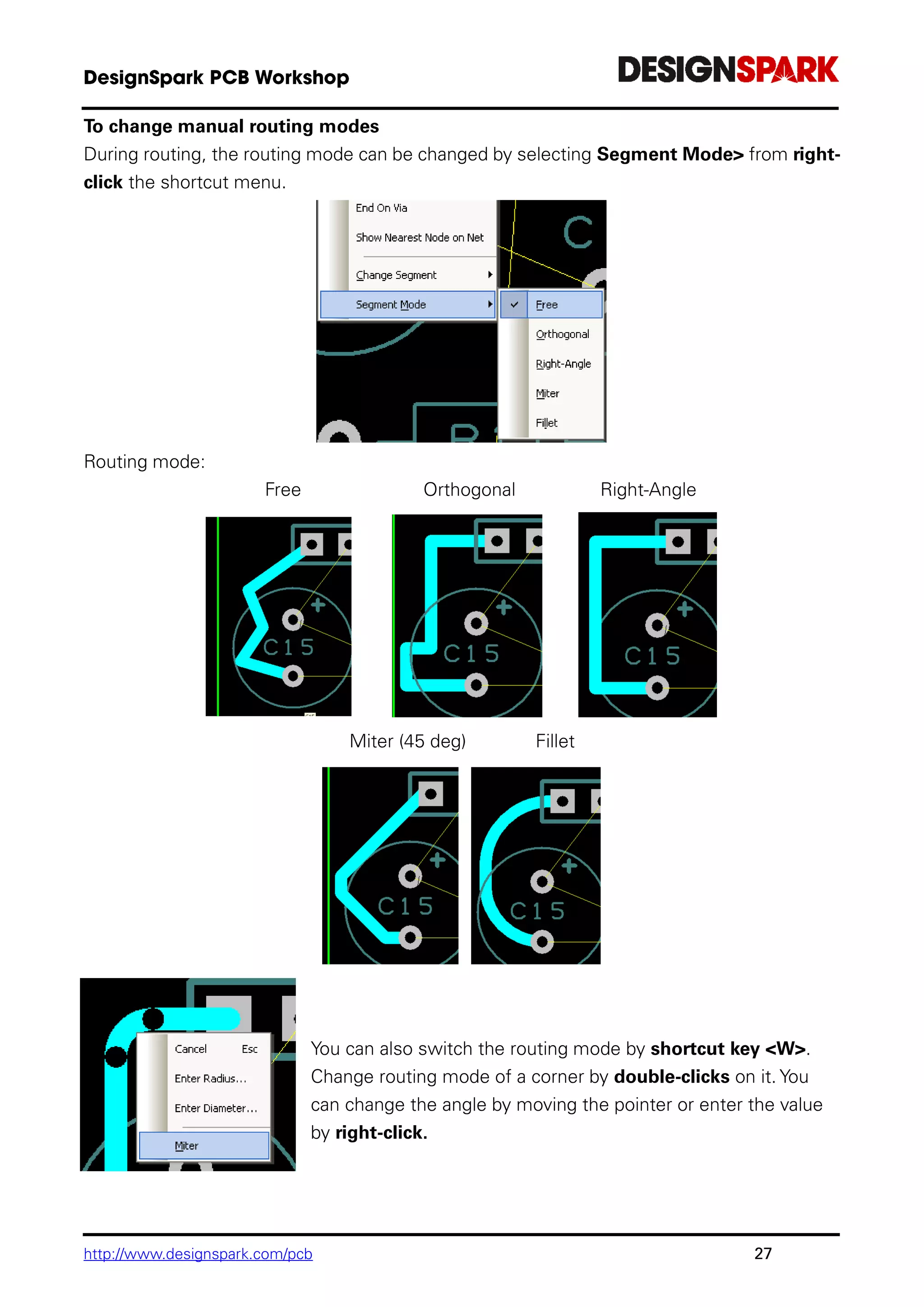
Enable MiterTrack in autorouter by check the box [MiterTrack].
Another dialog window will pop out to let you select the MITRE shape (Curved, any angle
or the default 45 deg) and specified the MITRE size.
Unrouting the design
The Unroute Nets> option is available on the Tools menu.
To unroute all nets, from Tools menu under Unroute Nets>, select All Nets.
You can always restore the routes using Undo<Ctrl-Z>.
Method 2: Manual Routing
Start routing track manually by double-click on the connection.
Single-Click, once editing, this will insert a corner to the change routing direction.
<L> followed by <Enter> will enable a layer change to the opposite side of the design. This
can be used during editing, or afterwards on selection of a track.
27. http://www.designspark.com/pcb 27
To change manual routing modes
During routing, the routing mode can be changed by selecting Segment Mode> from right-
click the shortcut menu.
Routing mode:
Free Orthogonal Right-Angle
Miter (45 deg) Fillet
You can also switch the routing mode by shortcut key <W>.
Change routing mode of a corner by double-clicks on it. You
can change the angle by moving the pointer or enter the value
by right-click.
28. http://www.designspark.com/pcb 28
To add via
When we have a close look at PCB board, you can easily notice these small holes, they are
via. The usage of such holes is to connect different layers.
When routing, we may meet the condition that we want two wires which located on
different layers to be connected together. Here we will need via.
First double-clicks on the pad to add connection.
Then left click once on the blank area, the wire we drew
before will be “locked”.
Then, change layer of the wire (L + enter).
We can see that via has been added automatically.
Wire on lower
layer
Via
Wire on upper
layer
Board
29. http://www.designspark.com/pcb 29
Delete vs Unroute
What should we do if we want to make some modification of the existing wire (an already
connected wire)? Sometimes we may follow the common sense, just select the wire and
Delete, however it is easy to make mistakes using such method if we are not careful
enough.
What is the difference between Delete and
Unroute? We will illustrate here.
For example, this is a connected wire. We want to
change it.
If we directly select the wire and Delete, you may
find the yellow instruction wire disappear. If you are
not careful enough, you may ignore the connection
and lead to unconnected net.
If we select the wire, then select Tools->
Unroute Nets->Selected Nets. After deleting
the old wire, the yellow instruction wire will
appear again to instruct you to connect the nets,
which may avoid some potential mistakes.
30. http://www.designspark.com/pcb 30
Some RoutingTips:
1. Refer to the schematic, place all the components wisely before starting to route. A good
layout may largely reduce your routing work and reduce the number of via. So we may refer
to the schematic for a clever placement. Eg. Some components with lots of common
connections can be placed closer in order to minimize the length of wires.
2. Consider the practical soldering requirement. We should not forget that designing a PCB
is for practical usage at final stage. So we should consider some practical issues. Eg. The
layout should be easy for soldering. For some full hole components, we should not place
other components too close to the hole. The size of the board, the position of screw holes
should all meet practical requirement.
3. Be careful about the width of the wire. Especially when you are dealing with the circuit
having large current. Wider wire can afford larger current. So the power wire or the wire for
motor will normally be wider.
The relationship between wire width and max current has been attached for your
reference.
Width(mm) Current(A)
0.2 0.5
0.3 0.75
0.5 1.25
1.25 2.5
2.5 4
5 7
8.12 10
4. Try to reduce the number of via, especially when you are dealing with signal wire. Via
will create extra delay for the signal due to parasitic effect. So we should avoid layer changing
when routing the signal wires so as to reduce the number of via.
5. It is acceptable for low frequency signal line to have 90 degree turn. But if you are dealing
with high frequency signals try to avoid having sharp corners when routing due to some
electromagnetic emission issues.
31. http://www.designspark.com/pcb 31
Cross Probe Overview
Cross Probe allows the user to simply click on the component in either view, which will then
immediately take them to the component in the counterpart view; the function works either
way from PCB to schematic or vice versa. This feature allows you to probe and locate items
in a known design. This enables better integration of design data between each stage of the
design process.
How to use Cross Probe
Cross Probe function is available from the Main Menu>Edit>Cross Probe or from the Cross
Probe Icon on Right-hand Toolbar. The shortcut key is <Shift X>. Cross probing is only
available in the PCB or Schematic design editors.
To use this option, a toolbar icon is available to put the application into the Cross Probe
'mode' prior to probing. There is also an entry on the Edit menu called Cross Probe which
selects the cross probe mode. Once this is selected the designs can be cross probed.
For more information about this function, please refer to this link: http://bit.ly/1tMbM1P
32. http://www.designspark.com/pcb 32
Pouring Copper into Area
Why copper pouring?
Copper pour is pouring copper into the blank area which don’t have wires or pads.
Copper pour is extremely useful for POWER-DND-separate board. By copper pouring, we
create a ground plane, which makes the area connected to GND larger, in this way we can
shield more noise. In our daily life, PCB working environment usually exists lots of
electronic signals. So it is necessary to use some method to reduce the noise. Pour copper
make the system connected to GND with larger area, when noises enter the system, they
are more likely to be imported to GND. This also applies to the noises produced inside the
system. Besides, copper may help heat dissipation.
However, copper pour may works like patch antenna, which may produce noise under
certain condition. Furthermore, too thick copper makes heat dissipation too fast, which lead
to the difficulty of soldering.
All in all, copper pour is not necessary for every design, it should be decided by the certain
condition.
33. http://www.designspark.com/pcb 33
To create a copper pour area, from the Add menu, select Copper Power Area> Rectangle.
Other pour area options are available.
1 Define copper pour area menu 2 Select pour copper from
shortcut
3 Select net associated (if any) 4 Poured copper had obeyed the spacing rule
Define the spacing when pour copper
You can change the spacing between the pour copper area and the pad, track and via, etc.
We change the space through Design Technology (Shift + T or General Toolbar), choose
Spacing in the Design Technology window.
34. http://www.designspark.com/pcb 34
Pour Keepout
There may exists some area we don’t what copper to be poured into such area. We can
define pour keepout area.
First, we add a Copper Pour Area which is exactly the same as what we did for pour
copper. Right click on the selected area, choose Properties. Tick the Pour Keepout. See
the figure below.
35. http://www.designspark.com/pcb 35
Checking the Design Integrity
To check the designs
You can use the Schematics/PCB Check option on the Tools menu at any time.
To bring Schematic Change into the PCB
Run Forward Design Changes option from the Tools menu will “push” Schematic
changes into PCB design.
To back annotate name changes to the Schematic
Using Back Annotation option from the Tools menu can pass back the change
made in PCB back to the Schematic.
36. http://www.designspark.com/pcb 36
Design Rule Checking
To run Design Rule Check, select the Design Rule Check button option from the toolbar.
To locate DRC error markers, using
Goto browser on the Interaction
bar by pressing the <F9> key.
Viewing Power Plane Layer
From the View menu, select Powerplane> option, Select Show.
Select the layer required, e.g. GND plane.
If GND layer is selected, the plane will like this:
37. http://www.designspark.com/pcb 37
Reports, Part Lists and Net Lists
You can generate reports where all vital aspects of the design can be output in detail.
The reports are all available on the Output menu.
In Schematic editor: In PCB design editor:
Select the report you wanted and click Run button.
38. http://www.designspark.com/pcb 38
The Plotting Dialog
From the Output menu, select Manufacturing Plots option.
Plots : Choose the plots and the plot selection for output.
Output : Choose the output type, layer choice, plot contents and scale.
Plot-Gen : Select Auto-generation, add new plots, delete plots and align plots with each
other.
To generate plot for manufacturing, you need to plot Gerber plots for the electrical and non-
electrical layers and Excellon NC drill files for drilling the board.
Plot Generation Area
Plot Area Output Area
39. http://www.designspark.com/pcb 39
Creating plots
Once all the parameters have been set for each plot, you can output them.
Use the Run button the create plots of all the plots in the Plots: list, the ones that have a
“tick” next to them.
Choose Options button on this page will bring you to new dialog as below. You can direct
the plot to a specific folder under Where Plot Files Are Written.
You can check the plot’s position, size, contents etc by checking the Plot Preview check
box.
40. http://www.designspark.com/pcb 40
BOM Quote interface that links DesignSpark PCB to the RS-online eCommerce website.
Instant price and availability, direct from your local RS website
Quotes can be downloaded, saved or forwarded on to colleagues for approvals or
completion
Leverages the world class ecommerce capabilities of rswww.com
On the upper right corner, click the BOM quote icon that connects us to the local RS
website.
All the components from your design listed with the information transferred from
DesignSpark PCB and the relevant component matches
41. http://www.designspark.com/pcb 41
Scrolling down to the bottom, you can download
the bill of materials, email it to a friend or a
colleague, or go directly to the order pad and
purchase our components by click Add Accepted
Items to Shopping Cart on the bottom right
corne
42. DesignSpark PCB Workshop
http://www.designspark.com/pcb 42
The libraries are made up of three individual libraries. There is a Component library made-up
of elements from the Schematic Symbol library and the PCB Symbol (footprint) library.
Library Manager is used to create and manage all your libraries.
43. DesignSpark PCB Workshop
http://www.designspark.com/pcb 43
Create new Schematic Symbol
To open the library manager
From the File toolbar, select the Libraries icon (shortcut Ctrl+L).
To open the symbol editor
From the Library Manager dialog, select the Schematic Symbols tab. Click New Lib and
type name Tutorial. This will be the name of your new library.
To create new schematic symbol, click New item.
44. DesignSpark PCB Workshop
http://www.designspark.com/pcb 44
Draw symbol using Add Closed Shape Icon
Draw lines using Add Shape Single Line Icon
Adding Pins using Add Pad Icon
Information on the pins
Each Pin contains three pieces of information:
- the big cross marking the shape and location of the pin
- the Pin Number (1, 2, 3 etc.)
- the pin name position marker, N1, N2, N3 etc. which marks the location of the pin name
when used on the Component in the design
Moving the symbol origin
The Symbol origin is the Symbol’s reference point used when moving it in the Schematic
design (the small ‘S’ marker, usually on Pin 1 of the symbol.
45. DesignSpark PCB Workshop
http://www.designspark.com/pcb 45
Select and drag the symbol origin to Pin 1 as shown below.
Adding the reference origin
Without a Reference Origin, the component name (U1, IC1 etc.) used in the Schematic
design will automatically be placed on the Symbol Origin. By adding a specific Reference
Origin you can position the Component name where you like.
To add the Reference Origin, select Reference Origin from the Add menu.
46. DesignSpark PCB Workshop
http://www.designspark.com/pcb 46
Saving the symbol
From the File menu, select Save.
Viewing the symbol in the library
From the File toolbar, select Libraries, you can also use the <Ctrl-L> shortcut key. Ensure
the Preview box is checked. From the Library Contents: list, select the OPAMP symbol
that you’ve created, it should look like the one below:
47. DesignSpark PCB Workshop
http://www.designspark.com/pcb 47
Create new PCB Symbol
Start the Library Manager
From the File toolbar, select the Libraries icon (shortcut Ctrl-L).
To open the symbol editor
From the Library manager dialog select the PCB Symbols tab. Click the New Lib button.
In the File name box, type New_PCB_LIB as your new PCB symbol library. Click Save to
accept this. The library manager is now ready to start entering new PCB symbols.
49. DesignSpark PCB Workshop
http://www.designspark.com/pcb 49
Click Next> to move on. Choose a possible Technology file and the Units to be used.
Click Next> to move on. Choose the footprint you wish to create.
You can select the Origin and Component Name Position in this window.
Click Next> to move on. The Pads page is used to define the overall footprint layout.
This is probably the most important page of the wizard. The default page setup is shown
below, we need to change the parameters defined here.
50. DesignSpark PCB Workshop
http://www.designspark.com/pcb 50
The Pad Count should be set to a Total of 10, use the spinner or type in the number.
You must type in the name of the pad style that will get saved once you’ve edited the
dimensions.
Use Rec 65 30 for this tutorial example.
You can now define the position for Pin 1 to be the bottom left corner, to Hide Pin numbers
and the Pin Numbering to be Counter-clockwise.
Click Next> to move on. You should now define the Silkscreen outline.
Select Top Silkscreen in the Layer: drop down box.
The only parameter to change here is the Notch At End value, change this to 0.50
51. DesignSpark PCB Workshop
http://www.designspark.com/pcb 51
Click Next> to move on. We will use the placement shape and add it to the Top Assembly
layer. Select this layer from the drop down list.
Click Next> to move on. In the Footprint Name: box, type RM-10.
Check the Save the footprint to the library box.
Select your New_PCB_Lib.psl library from the drop down list.
Leave the Edit the footprint now check box unchecked.
Click Finish to complete the footprint creation.
52. DesignSpark PCB Workshop
http://www.designspark.com/pcb 52
Viewing the symbol in the library
Now that the symbol has been created and saved, let’s view it in the library manager.
Click <Ctrl-S> to save the footprint.
From the Libraries button on the File toolbar, select Libraries, shortcut key <F11>.
Select the newly created footprint from the contents list (RM-10). Check the Preview box
if not already selected so you can view the footprint. You can also edit it from here as well.
53. DesignSpark PCB Workshop
http://www.designspark.com/pcb 53
Create new Component Symbol
Using the Component Editor
This tutorial uses the Schematic Symbol and PCB Symbol (Footprint) created in the
previous sections, but equally applies to creating a component using other Schematic
Symbols and PCB Symbols.
To open the Component editor
On the File toolbar click Libraries <F11> or <Ctrl-L>.
To open the symbol editor
From the Library manager dialog select the Components tab. Click the New Lib button.
In the File name box, type New_COMP_lib as your new component library. Click Save to
accept this. The library manager is now ready to start entering new components.
54. DesignSpark PCB Workshop
http://www.designspark.com/pcb 54
Click on New Item
The New Component dialog opens.
There are 8 pieces of information required:
In the Component: box type the component name AD8592RM
In the Package: box, type SOIC, this identifies the package type, multiple package
types can be used for selecting alternative footprints. This doesn’t appear in the list
until you type it in.
In the Default Reference: box type U. This will be the component name used in
the actual design
(U1, IC1, R1, C1 etc.)
For Schematic Symbol, ensure that the library is set to New_sch_lib.psl.
Select your Schematic Symbol previously created OPAMP from the list.
The dialog will automatically show Pins: as 3 (3 pins on the gate created) and
Gates: as 1. Change the Gates: to 2.
55. DesignSpark PCB Workshop
http://www.designspark.com/pcb 55
For PCB Symbol, ensure that the library is set to New_COMP_lib.ssl. Select your
PCB Symbol previously created RM-10.
Once it does, click OK to continue. The Component Editor opens showing the items
added from the New Component dialog.
56. DesignSpark PCB Workshop
http://www.designspark.com/pcb 56
Adding an extra gate
We need to add a power gate to the component.
Right click anywhere in the component grid. From the list, select Edit Gates.
From the Gates dialog, select the Add button. Notice your existing 2x OPAMP gates are
already
shown in the list as gates a & b.
From the Library: list select the AD.ssl library.
Scroll down the Name: list and select the AD-P2 gate symbol. Ensure that you only have 1
selected
in the Add 1 Gates box. Click the Add button.
The Power gate will appear at the bottom of the list. Click OK to add it to the component.
57. DesignSpark PCB Workshop
http://www.designspark.com/pcb 57
Map pins to pads
Click on the Assign Pins button on the Component toolbar.
Select Pin 3 on the Schematic Symbol. Select Pad 1 on the PCB Symbol.
The component grid will display the number 1 for Sch Terminal Number 3 on gate a, it
will also display a number 1 in the corresponding Component Pin Name/Number cell.
Adding Logic Names to your Component
To add or edit Logic Names to a Component in the editor (using our existing example
which should still be open), type in the names required into the Sch Symbol Terminal
Names field.
58. DesignSpark PCB Workshop
http://www.designspark.com/pcb 58
Adding Values to your Component
To add or edit values to a component in the editor, from the Edit menu select Values.
Click Add to create a new value.
From the Add dialog you can type the Name and Value: You do not have to add a value at
this stage, the name can be left ‘empty’ to be fulfilled at a later stage or during design.
Click OK to confirm the selection.
Saving your Component
From the File toolbar, select Save <Ctrl-S>. The Save To Library dialog opens. Choose the
New_COMP_lib.cml library from the list if not already selected.
Click OK to confirm the library name and component name. You have now saved the
Component in the Library. The component will still be visible in the editor.
59. DesignSpark PCB Workshop
http://www.designspark.com/pcb 59
Viewing the Component in the library
From the File toolbar, select Libraries, <F11> or <Ctrl-L>. The Libraries dialog opens.
Make sure the Preview box is checked. Select the Components tab. Select the AD8592RM
Component that you created, it should look like the one below.
A quick check to whether you have created is correctly is the existence of both the Schematic
and PCB Symbols in their respective Preview windows. At this stage, you would add this
component to a Schematic or PCB design and it would work.
DesignSpark PCB can be linked to industry standard Spice simulators to carry out circuit
simulation. By following a few simple rules you can create your Schematic circuit in
DesignSpark, then use a simulator to verify its operation before moving on to the next stage
of your project.
DesignSpark PCB currently supports four simulators : LTSpice, LSSpice, B2Spice and TINA.
60. DesignSpark PCB Workshop
http://www.designspark.com/pcb 60
To open the Spice Interface
From the Output toolbar, select the Spice Simulation Output
Select the Simulator Format, in the Run simulator : box, enter your simulator execute
path.
Enter your simulation parameter in each tabs, click OK to run your Simulator.
62. DesignSpark PCB Workshop
http://www.designspark.com/pcb 62
You can select tracks or vias in your design and perform basic electrical calculations on
them such as:
width of a track required for a given current
impedance of a selected track
optimum copper density to use
approximate temperature rise on a track
resistance of a via given its physical characteristics
These useful calculators produce approximations of actual circuit performance to aid your
decision process in completing a successful layout.
To open the Design Calculators,
From the Tools toolbar, select the Design Calculators
You can use the Design Calculators to perform basic electrical calculations.
63. DesignSpark PCB Workshop
http://www.designspark.com/pcb 63
1. DesignSpark PCBTutorials (Pre-installed with DSPCB V4)
Forums
https://designspark.zendesk.com/hc/en-us/community/topics/200624545-DesignSpark-PCB-
Discussion
Tutorials and Support Centre
https://designspark.zendesk.com/hc/en-us/categories/201145765
Catalogue of Reference Designs
https://www.rs-online.com/designspark/reference-designs
Sparkfun Libraries including libraries of Arduino shields
http://bit.ly/15rEZox
Shared libraries in DesignSpark
http://www.neatinfo.com/designspark/
http://www.designspark.com/pcb
http://www.facebook.com/DesignSparkRS (Eng)
https://www.facebook.com/DSChinese (中文)
http://weibo.com/designsparkcn
http://www.youtube.com/user/DesignSpark
http://www.youtube.com/user/DesignSparkHK (HK Cantonese Channel)
http://www.tudou.com
http://i.youku.com/designsparkcn
64. DesignSpark PCB Workshop
http://www.designspark.com/pcb 64
Label Ref Component Value Qty Library
Schematic
Symbol
Desc
1 R1 R 1K 1 Designspark.cml R Resistor
2 R2 R 2K 1 Designspark.cml R Resistor
3 C1 C 10uF 1 Designspark.cml Capacitor_Pol Capacitor
4 C2 C 100nF 1 Designspark.cml Capacitor Capacitor
5 C3 C 10uF 1 Designspark.cml Capacitor Capacitor
6 U1 NE555N 1 st.cml NE555N Timer
7 U2 SN74ALS74AD 1 ti.cml SN74ALS74AD Flip Flop
8 PL1 Connectors 1 Designspark.cml CONN_SIL_2 2 pin header
9 PL2 Connectors 1 Designspark.cml CONN_SIL_3 3 pin header
10 Vcc Symbol 3 Designspark.cml Vcc Power
11 GND Symbol 3 Designspark.cml GND Power
12 MCLK 3 MCLK Net name
13 MCLK_2 2 MCLK_2 Net name
14 MCLK_4 2 MCLK_4 Net name
1
2
3
4
5
6
7
8 9
10
11
12
13
14