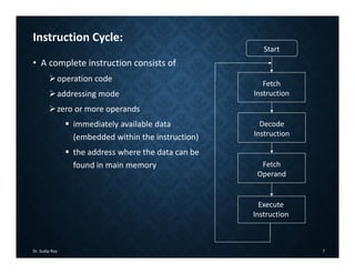
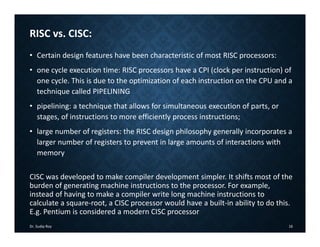
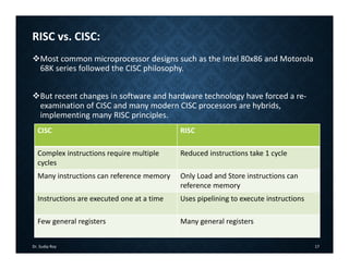
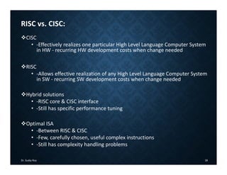
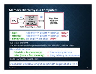
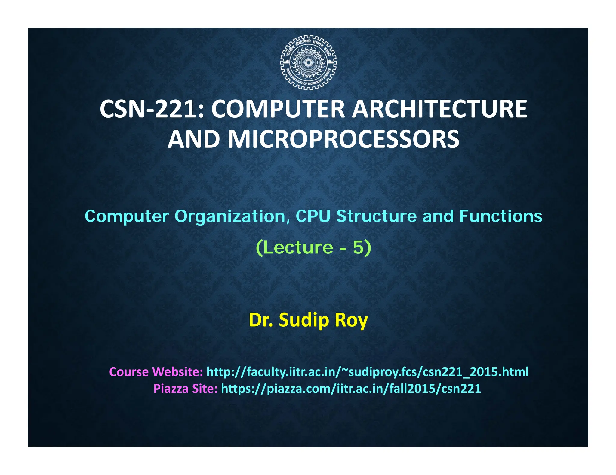
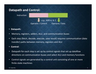
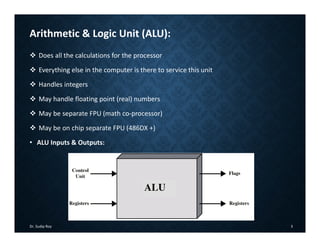
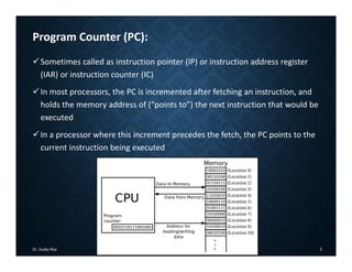
Dr. Sudip Roy's course CSN-221 covers computer architecture and microprocessors, focusing on datapath and control, instruction cycles, and the differences between RISC and CISC architectures. Key components like the ALU, instruction set architecture, and memory hierarchy are discussed, along with the operation of control units and the importance of efficient circuit design. The document outlines the evolution of microprocessor design philosophies, emphasizing the need for optimized instruction execution through techniques like pipelining.

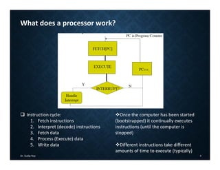
![Example: Instruction Execution
• MULT x, y, product
1. Fetch the instruction code from Memory[PC]
2. Decode the instruction. This reveals that it's a multiply instruction, and that
the operands are memory locations x, y, and product.
3. Fetch x and y from memory.
4. Multiply x and y, storing the result in a CPU register.
5. Save the result from the CPU to memory location product.
Dr. Sudip Roy 6](https://image.slidesharecdn.com/csn221lec5-240625145904-be99b335/85/CSN221_Lec_5-pdf-Computer-Organization-CPU-Structure-and-Functions-6-320.jpg)