The document discusses how computers represent data digitally using binary numbers. It explains that computers use groups of 8 bits called bytes to store each character, number, or symbol. The ASCII table assigns a unique 8-bit binary number to each character, allowing all text, numbers, and punctuation to be stored and processed as digital data composed of bytes consisting of 0s and 1s. Programs and files on computers are also represented using this system, with file extensions helping identify different data types.
![KarbosGuide.com. Module 1a. About data.
With our electric switches, we can write 0 or 1. We can now start our data processing!
The PC is filled with these switches (in the form of transistors). There are literally millions of those in the
electronic components. Each represents either a 0 or a 1, so we can process data with millions of 0s and
1s.
Please click the banners to support our work!
Bits
[top]
Each 0 or 1 is called a bit. Bit is an abbreviation of the expression BInary digiT. It is called binary, since
it is derived from the binary number system:
0 1 bit
http://www.karbosguide.com/hardware/module1a1.htm (2 of 5)7/27/2004 4:05:11 AM](https://image.slidesharecdn.com/computerhardware-michaelkarbo-121118154249-phpapp01/75/Computer-hardware-michael-karbo-2-2048.jpg)
![KarbosGuide.com. Module 1a. About data.
1 1 bit
0110 4 bit
01101011 8 bit
The binary number system
[top]
The binary number system is made up of digits, just like our common decimal system (10 digit system).
But, while the decimal system uses digits 0 through 9, the binary system only uses digits 0 and 1.
If you are interested in understanding the binary number system, then here is a brief course. See if you
can follow the system. See how numbers are constructed in the binary system, using only 0s and 1s:
Numbers, as known in the Same numbers in binary
decimal-system system
0 0
1 1
2 10
3 11
4 100
5 101
6 110
7 111
8 1000
Digital data
[top]
http://www.karbosguide.com/hardware/module1a1.htm (3 of 5)7/27/2004 4:05:11 AM](https://image.slidesharecdn.com/computerhardware-michaelkarbo-121118154249-phpapp01/75/Computer-hardware-michael-karbo-3-2048.jpg)
![KarbosGuide.com. Module 1a. About data.
We have seen that the PC appears capable of handling data, if it can receive them as 0s and 1s. This
data format is called digital. If we can translate our daily data from their analog format to digital format,
they will appear as chains of 0s and 1s, then the PC can handle them.
So, we must be able to digitize our data. Pour text, sounds, and pictures into a funnel, from where they
emerge as 0s and 1s:
Let us see how this can be accomplished.
q Next page
q Previous page
Learn more [top]
Read more about the boot process and system bus in Module 2b
Read more about I/O buses in module 2c
Read more about the motherboard chip set in module 2d
Read more about RAM in module 2e
Read about EIDE in module 5b
[Main page] [Contact] [Karbo's Dictionary] [The Software Guides]
http://www.karbosguide.com/hardware/module1a1.htm (4 of 5)7/27/2004 4:05:11 AM](https://image.slidesharecdn.com/computerhardware-michaelkarbo-121118154249-phpapp01/75/Computer-hardware-michael-karbo-4-2048.jpg)
![KarbosGuide.com. Module 1a. About data.
"translation:"
Character Bit pattern Byte Character Bit pattern Byte
number number
A 01000001 65 ¼ 10111100 188
B 01000010 66 . 00101110 46
C 01000011 67 : 00111010 58
a 01100001 97 $ 00100100 36
b 01100010 98 01011100 92
o 01101111 111 ~ 01111110 126
p 01110000 112 1 00110001 49
q 01110001 113 2 00110010 50
r 01110010 114 9 00111001 57
x 01111000 120 © 10101001 169
y 01111001 121 > 00111110 62
z 01111010 122 ‰ 10001001 137
When you write the word "summer", you write 6 letters. If the computer has to process that
word, it will be digitized to 6 bytes. In other words, the word summer occupies 6 bytes in the
PC RAM, when you type it, and 6 bytes on the hard disk, if you save it.
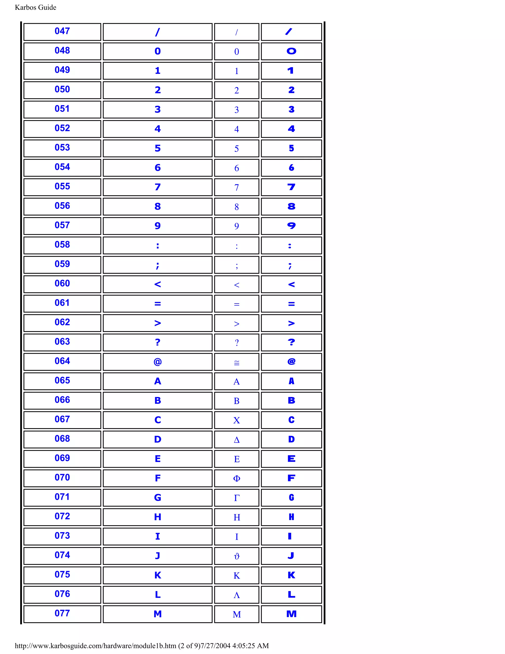
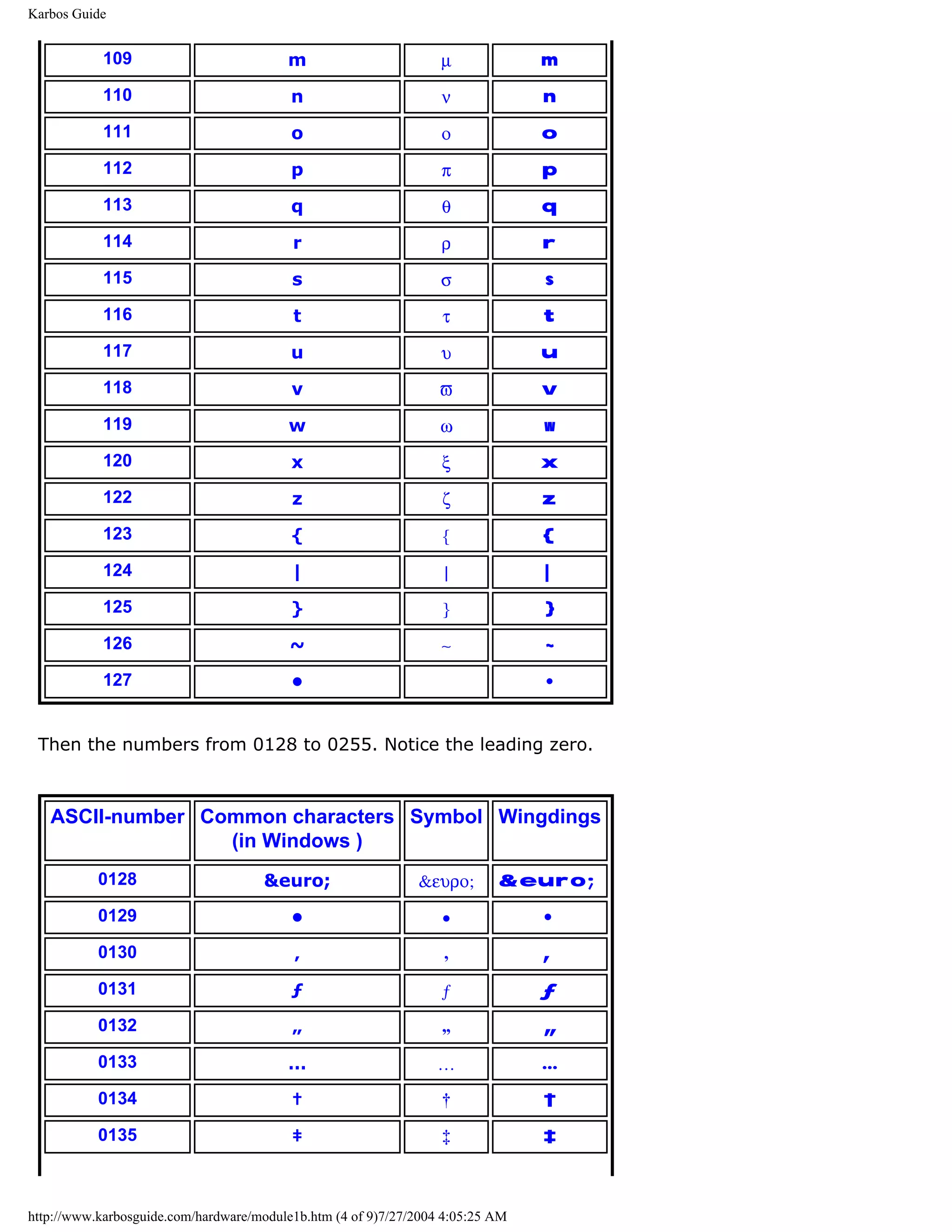
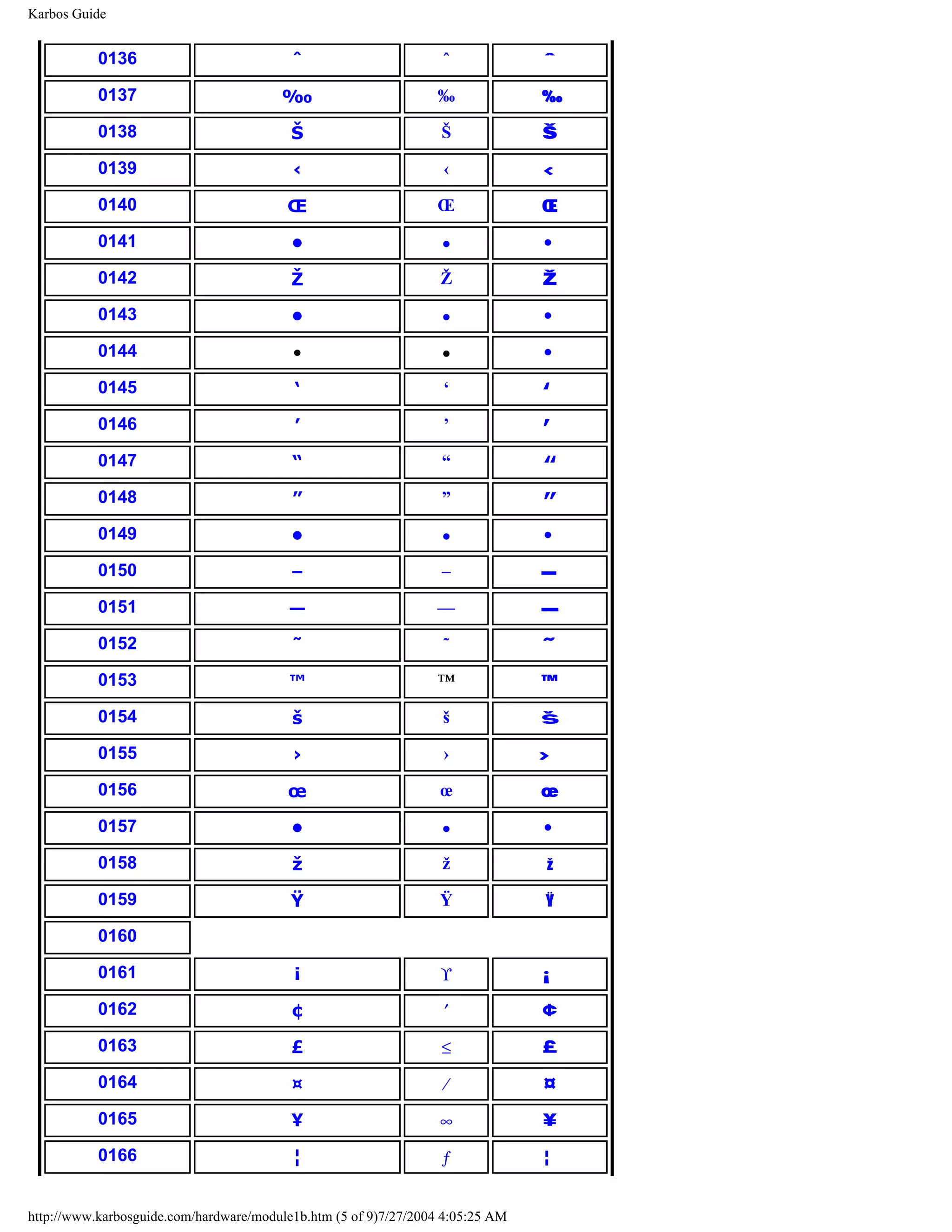
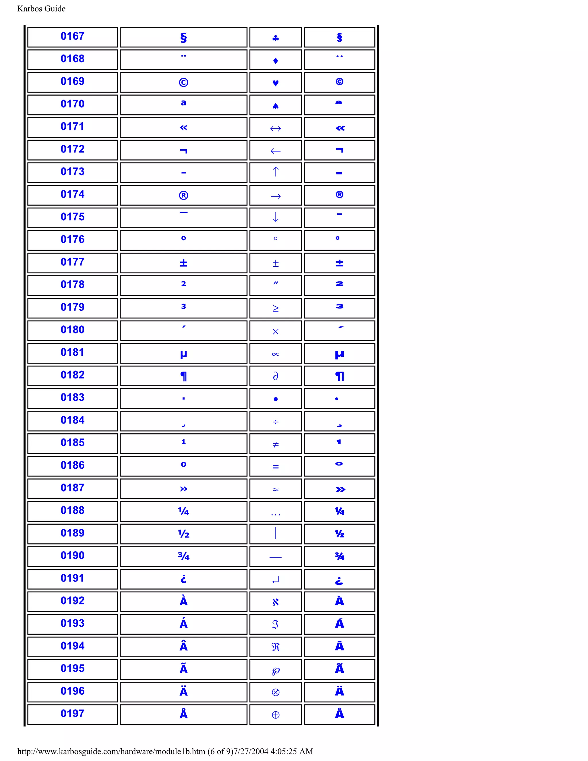
ASCII
[top]
ASCII means American Standard Code for Information Interchange. It is an industry
standard, which assigns letters, numbers, and other characters within the 256 slots available
in the 8 bit code.
http://www.karbosguide.com/hardware/module1a2.htm (2 of 5)7/27/2004 4:05:22 AM](https://image.slidesharecdn.com/computerhardware-michaelkarbo-121118154249-phpapp01/75/Computer-hardware-michael-karbo-7-2048.jpg)
![KarbosGuide.com. Module 1a. About data.
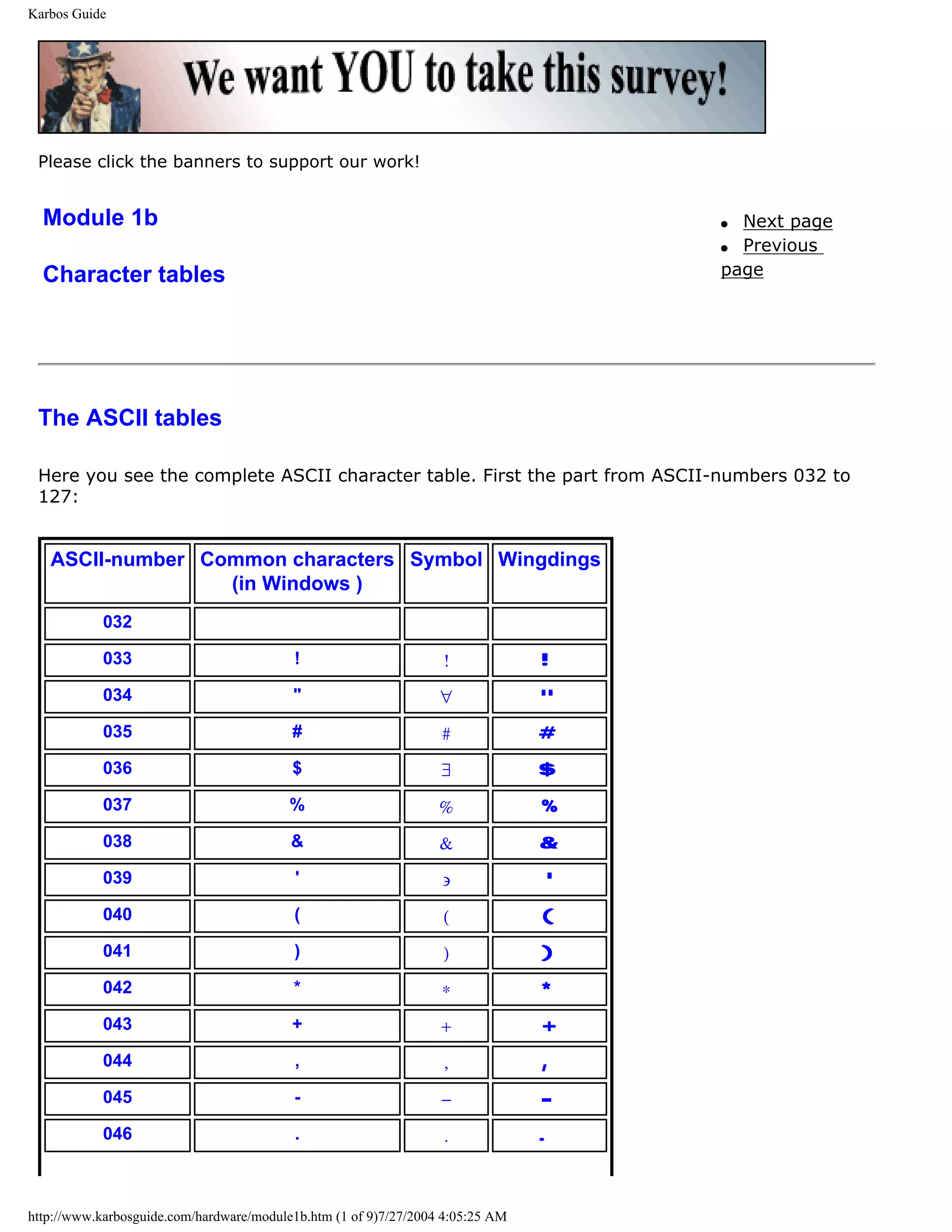
The ASCII table is divided in 3 sections:
q Non printable system codes between 0 and 31.
q "Lower ASCII" between 32 and 127. This part of the table originates from older, American
systems, which worked on 7 bit character tables. Foreign letters, like Ø and Ü were not
available then.
q "Higher ASCII" between 128 and 255. This part is programmable, in that you can
exchange characters, based on which language you want to write in. Foreign letters are
placed in this part.
Learn more about the ASCII table in Module 1b
An example
Let us imagine a stream of bits sent from the keyboard to the computer. When you type,
streams of 8 bits are sent to the computer. Let us look at a series of bits:
001100010011001000110011
Bits are combined into bytes (each 8 bits). These 24 bits are interpreted as three bytes. Let
us read them as bytes: 00110001, 00110010, and 00110011.
When we convert these byte binary numbers to decimal numbers, you will see that they read
as 49, 50, and 51 in decimal numbers. To interpret these numbers, we have to look at the
ASCII table. You will find that you have typed the numbers 1, 2, and 3.
About text and code
[top]
Now we have seen the PCs user data, which are always digitized. But there are many
different kinds of data in the PC. You can differentiate between 2 fundamental types of data:
q Program code, which is data, that allows the PC to function.
q User data, like text, graphics, sound.
The fact is, that the CPU must have instructions to function. You can read more about this in
the review of the CPU in module 3a. An instruction is a string of data, of 0s and 1s. The CPU
is designed to recognize these instructions, which arrive together with the user input data to
http://www.karbosguide.com/hardware/module1a2.htm (3 of 5)7/27/2004 4:05:22 AM](https://image.slidesharecdn.com/computerhardware-michaelkarbo-121118154249-phpapp01/75/Computer-hardware-michael-karbo-8-2048.jpg)
![KarbosGuide.com. Module 1a. About data.
be processed.
The program code is thus a collection of instructions, which are executed one by one, when
the program runs. Each time you click the mouse, or hit a key on the keyboard, instructions
are sent from your software (program) to the CPU, telling it what to do next.
User data are those data, which tells the software how to respond. The letters, illustrations,
home pages, etc., which you and I produce, are created with appropriate software.
Files
[top]
Both program code and user data are saved as files on the hard disk. Often, you can
recognize the type of file by its suffix. Here are some examples:
Content File name
Program code START.EXE, WIN.COM, HELP.DLL, VMM32.VXD
User data LETTER.DOC, HOUSE.BMP, INDEX.HTM
This is written as an introduction to naming files. The file name suffix determines how the PC
will handle the file. You can read about this subject in some of my books, e.g. "DOS - teach
yourself" (only available in Europe.
q Next page
q Previous page
Learn more [top]
Read more about the boot process and system bus in Module 2b
Read more about I/O buses in module 2c
Read more about the motherboard chip set in module 2d
Read more about RAM in module 2e
http://www.karbosguide.com/hardware/module1a2.htm (4 of 5)7/27/2004 4:05:22 AM](https://image.slidesharecdn.com/computerhardware-michaelkarbo-121118154249-phpapp01/75/Computer-hardware-michael-karbo-9-2048.jpg)
![KarbosGuide.com. Module 1a. About data.
Read about EIDE in module 5b
[Main page] [Contact] [Karbo's Dictionary] [The Software Guides]
Copyright (c) 1996-2001 by Michael B. Karbo. www.karbosguide.com.
http://www.karbosguide.com/hardware/module1a2.htm (5 of 5)7/27/2004 4:05:22 AM](https://image.slidesharecdn.com/computerhardware-michaelkarbo-121118154249-phpapp01/75/Computer-hardware-michael-karbo-10-2048.jpg)
![Karbos Guide
078 N Ν N
079 O Ο O
080 P Π P
081 Q Θ Q
082 R Ρ R
083 S Σ S
084 T Τ T
085 U Υ U
086 V ς V
087 W Ω W
088 X Ξ X
089 Y Ψ Y
090 Z Ζ Z
091 [ [ [
092 ∴
093 ] ] ]
094 ^ ⊥ ^
095 _ _ _
096 ` `
097 a α a
098 b β b
099 c χ c
100 d δ d
101 e ε e
102 f φ f
103 g γ g
104 h η h
105 i ι i
106 j ϕ j
107 k κ k
108 l λ l
http://www.karbosguide.com/hardware/module1b.htm (3 of 9)7/27/2004 4:05:25 AM](https://image.slidesharecdn.com/computerhardware-michaelkarbo-121118154249-phpapp01/75/Computer-hardware-michael-karbo-13-2048.jpg)
![Karbos Guide
Learn more [top]
Read module 5a about expansion cards, where we evaluate the I/O buses from the port side.
Read module 5b about AGP and module 5c about Firewire.
Read module 7a about monitors, and 7b on graphics card.
Read module 7c about sound cards, and 7d on digital sound and music.
[Main page] [Contact] [Karbo's Dictionary] [The Software Guides]
Copyright (c) 1996-2001 by Michael B. Karbo. www.karbosguide.com.
http://www.karbosguide.com/hardware/module1b.htm (9 of 9)7/27/2004 4:05:25 AM](https://image.slidesharecdn.com/computerhardware-michaelkarbo-121118154249-phpapp01/75/Computer-hardware-michael-karbo-19-2048.jpg)
![An illustrated Guide to Motherboards
Please click the banners to support our work!
The PC's success [top]
The PC came out in 1981. In less than 20 years, it has totally changed our means of communicating. When the PC was
introduced by IBM, it was just one of many different micro data processors. However, the PC caught on. In 5-7 years,
it conquered the market. From being an IBM compatible PC, it became the standard.
If we look at early PCs, they are characterized by a number of features. Those were instrumental in creating the PC
success.
q The PC was from the start standardized and had an open architecture.
q It was well documented and had great possibilities for expansion.
q It was inexpensive, simple and robust (definitely not advanced).
The PC started as IBM's baby. It was their design, built over an Intel processor (8088) and fitted to Microsoft's simple
operating system MS-DOS.
Since the design was well documented, other companies entered the market. They could produce functionable copies
(clones) of the central system software (BIOS). The central ISA bus was not patented. Slowly, a myriad of companies
developed, manufacturing IBM compatible PCs and components for them.
The Clone was born. A clone is a copy of a machine. A machine, which can do precisely the same as the original (read
Big Blue - IBM). Some of the components (for example the hard disk) may be identical to the original. However, the
Clone has another name (Compaq, Olivetti, etc.), or it has no name at all. This is the case with "the real clones."
Today, we differentiate between:
q Brand names, PCs from IBM, Compaq, AST, etc. Companies which are so big, so they develop their own hardware
components.
q Clones, which are built from standard components. Anyone can make a clone.
Since the basic technology is shared by all PCs, I will start with a review of that.
The PC construction
[top]
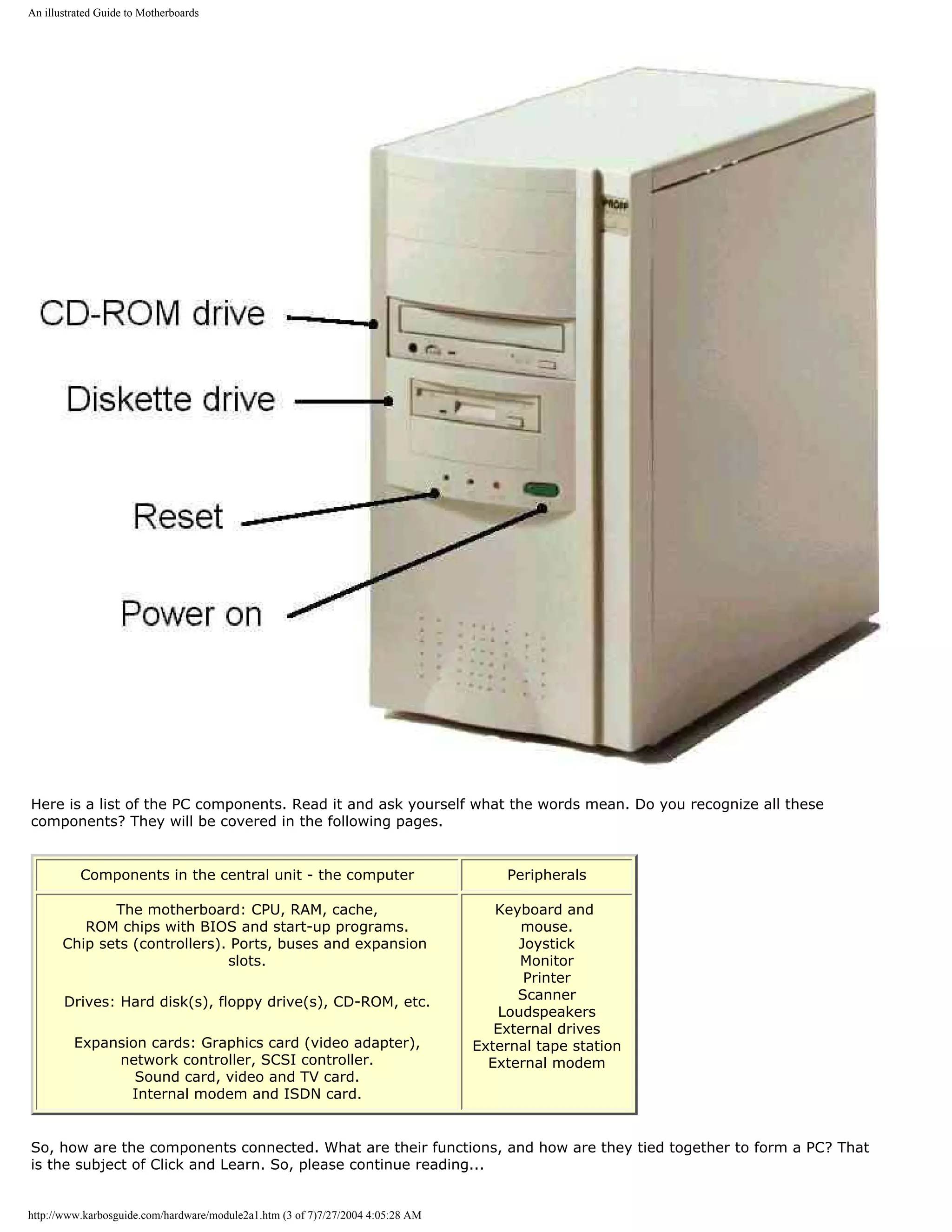
The PC consists of a central unit (referred to as the computer) and various peripherals. The computer is a box, which
contains most of the working electronics. It is connected with cables to the peripherals.
On these pages, I will show you the computer and its components. Here is a picture of the computer:
http://www.karbosguide.com/hardware/module2a1.htm (2 of 7)7/27/2004 4:05:28 AM](https://image.slidesharecdn.com/computerhardware-michaelkarbo-121118154249-phpapp01/75/Computer-hardware-michael-karbo-21-2048.jpg)
![An illustrated Guide to Motherboards
The von Neumann Model of the PC
[top]
Computers have their roots 300 years back in history. Mathematicians and philosophers like Pascal, Leibnitz, Babbage
and Boole made the foundation with their theoretical works. Only in the second half of this century was electronic
science sufficiently developed to make practical use of their theories.
The modern PC has roots that go back to the USA in the 1940s. Among the many scientists, I like to remember John
von Neumann (1903-57). He was a mathematician, born in Hungary. We can still use his computer design today. He
broke computer hardware down in five primary parts:
q CPU
q Input
q Output
q Working memory
q Permanent memory
Actually, von Neumann was the first to design a computer with a working memory (what we today call RAM). If we
apply his model to current PCs, it will look like this:
http://www.karbosguide.com/hardware/module2a1.htm (4 of 7)7/27/2004 4:05:28 AM](https://image.slidesharecdn.com/computerhardware-michaelkarbo-121118154249-phpapp01/75/Computer-hardware-michael-karbo-23-2048.jpg)
![An illustrated Guide to Motherboards
All these subjects will be covered.
Data exchange - the motherboard
[top]
The ROM chips contain instructions, which are specific for that particular motherboard. Those programs and
instructions will remain in the PC throughout its life; usually they are not altered.
Primarily the ROM code holds start-up instructions. In fact there are several different programs inside the start-up
instructions, but for most users, they are all woven together. You can differentiate between:
q POST (Power On Self Test)
q The Setup instructions, which connect with the CMOS instructions
q BIOS instructions, which connect with the various hardware peripherals
q The Boot instructions, which call the operating system (DOS, OS/2, or Windows )
All these instructions are in ROM chips, and they are activated one by one during start-up. Let us look at each part.
The suppliers of system software
[top]
All PCs have instructions in ROM chips on the motherboard. The ROM chips are supplied by specialty software
manufacturers, who make BIOS chips. The primary suppliers are:
q Phoenix
q AMI ( American Megatrends )
q Award
You can read the name of your BIOS chip during start-up. You can also see the chip on the system board. Here is a
picture (slightly blurred) of an Award ROM chip:
http://www.karbosguide.com/hardware/module2a1.htm (5 of 7)7/27/2004 4:05:28 AM](https://image.slidesharecdn.com/computerhardware-michaelkarbo-121118154249-phpapp01/75/Computer-hardware-michael-karbo-24-2048.jpg)
![An illustrated Guide to Motherboards
Here is an AMI chip with BIOS and start-up instructions:
Let us look at the different components inside the ROM chip.
q Next page
q Previous page
Learn more [top]
Read more about the boot process and system bus in Module 2b
Read more about I/O buses in module 2c
Read more about the motherboard chip set in module 2d
Read more about RAM in module 2e
Read about EIDE in module 5b
I also recommend two books for further studies. Gunnar Forst: "PC Principles", from MIT is excellent. Also "The Winn
L. Rosch Hardware Bible" from Brady covers the same subjects. Also "PC Intern" from Abacus is fine.
Links to BIOS information:
Mr BIOS FAQ
http://www.karbosguide.com/hardware/module2a1.htm (6 of 7)7/27/2004 4:05:28 AM](https://image.slidesharecdn.com/computerhardware-michaelkarbo-121118154249-phpapp01/75/Computer-hardware-michael-karbo-25-2048.jpg)
![An illustrated Guide to Motherboards
[Main page] [Contact] [Karbo's Dictionary] [The Software Guides]
Copyright (c) 1996-2001 by Michael B. Karbo. www.karbosguide.com.
http://www.karbosguide.com/hardware/module2a1.htm (7 of 7)7/27/2004 4:05:28 AM](https://image.slidesharecdn.com/computerhardware-michaelkarbo-121118154249-phpapp01/75/Computer-hardware-michael-karbo-26-2048.jpg)
![An illustrated Guide to Motherboards
Please click the banners to support our work!
Click & Learn. Module 2a.2
The system software on the motherboard
The contents:
q The Setup program q Next page
q The POST q Previous page
q The CMOS RAM
q Opening the Setup program
Articles written
by Michael B. Karbo
The Setup programs [top]
There are three elements in the start-up part of the ROM chip:
q The Initializing routine, which sets up the BIOS functions. The adapter ROM is integrated. A
table covering all the BIOS programs is constructed. This is often called the interrupt vectors.
q The POST (the test programs)
q The disk bootstrap loader, which calls upon the operating system.
http://www.karbosguide.com/hardware/module2a2.htm (1 of 7)7/27/2004 4:05:35 AM](https://image.slidesharecdn.com/computerhardware-michaelkarbo-121118154249-phpapp01/75/Computer-hardware-michael-karbo-27-2048.jpg)
![An illustrated Guide to Motherboards
These programs are stored in the ROM chip, and they are activated one by one during the PC start-
up.
The POST
Power On Self Test is the first instruction executed during start-up. It checks the PC components
and that everything works. You can recognize it during the RAM test, which occurs as soon as you
turn power on.
You may follow the checks being executed in this order, as the information are gathered:
1) Information about the graphics adapter
2) Information about the BIOS (name, version)
3) Information about the RAM (being counted)
As users, we have only limited ability to manipulate the POST instructions. But certain system
boards enable the user to order a quick system check. Some enable the user to disable the RAM
test, thereby shortening the duration of the POST. The duration of the POST can vary considerably
in different PCs. On the IBM PC 300 computer, it is very slow. But you can disrupt it by pressing
[Esc].
Error messages
If POST detects errors in the system, it will write error messages on the screen. If the monitor is
not ready, or if the error is in the video card, it will also sound a pattern of beeps (for example 3
short and one long) to identify the error to the user. If you want to know more of the beeps, you
can find explanations on the Award, AMI and Phoenix web sites. For instance you will receive error
messages if the keyboard is not connected or if something is wrong with the cabling to the floppy
drive.
POST also reads those user data, which are found in the CMOS. This is discussed in the following
chapter.
The bootstrap loader
The last part of the BIOS execution at start-up is the bootstrap loader. It is a tiny program, which
only has one task: to find the bootsector on a disk (hard disk, floppy or another boot-drive).
The DOS Boot Record (DBR) also holds a media descriptor as well as information on the OS
version. Please read module 6a4 on this issue. You can use DiskEdit (included in the "Norton
Utilities") to read view the contents of the boot sector.
http://www.karbosguide.com/hardware/module2a2.htm (2 of 7)7/27/2004 4:05:35 AM](https://image.slidesharecdn.com/computerhardware-michaelkarbo-121118154249-phpapp01/75/Computer-hardware-michael-karbo-28-2048.jpg)
![An illustrated Guide to Motherboards
When the disk holds no boot strap routine, you get an error message like "Non-system disk,
replace with system disk and press any key".
The bootstrap loader is the last step in BIOS execution during start-up. It hands over the control to
the bootstrap routine found on the boot disk. The OS is being loaded.
CMOS RAM [top]
CMOS stands for Complementary Metal Oxide Semiconductor. In PC’s there is a small amount of
memory in a special CMOS RAM chip. The data is maintained with electric power from a small
battery.
CMOS is only a medium for storage. It could be used for any type of data. Here, it holds important
system data, values to be used during the start process. These information take up maybe 100 or
http://www.karbosguide.com/hardware/module2a2.htm (3 of 7)7/27/2004 4:05:35 AM](https://image.slidesharecdn.com/computerhardware-michaelkarbo-121118154249-phpapp01/75/Computer-hardware-michael-karbo-29-2048.jpg)
![An illustrated Guide to Motherboards
The configuration of CMOS data
The PC must be configured, be supplied with this information. That is done in the factory or store,
where it is assembled. This information is stored in CMOS, where they stay. CMOS data only need
to be updated, when different or additional hardware components are installed. This could be a
different type hard disk or floppy disks or an new RAM type. Often the user can do this him/herself.
Other data in CMOS contain various user options . This is data, which you can write to CMOS. For
example, you can adjust date and time, which the PC then adjusts every second. You can also
choose between different system parameters. Maybe you want a short system check instead of a
long one. Or if you want the PC to try to boot from hard disk C before trying floppy disk A, or vice
versa. These options can be written to CMOS.
Many of the options are of no interest to the ordinary user. These are options, which regard
controller chips on the motherboard, which can be configured in different ways. Ordinarily, there is
no need to make such changes. The motherboard manufacturer has already selected the optimal
configurations. They recommend in their manuals, that you do not change these default settings.
We can conclude, that CMOS data are essential system data, which are vital for operation of the
PC. Their special feature is, that they are user adjustable. Adjustments to CMOS are made during
start-up.
Opening the Setup program
[top]
You communicate with the BIOS programs and the CMOS memory through the so-called Setup
program. This gives us a very simple user interface to configuring the PC with these vital data.
Typically you reach the Setup program by pressing [Delete] immediately after you power up the
PC. That brings you to a choice of setup menus. You leave Setup by pressing [Esc], and choose "Y"
to restart the PC with the new settings. Generally, you should not change these settings, unless
http://www.karbosguide.com/hardware/module2a2.htm (5 of 7)7/27/2004 4:05:35 AM](https://image.slidesharecdn.com/computerhardware-michaelkarbo-121118154249-phpapp01/75/Computer-hardware-michael-karbo-31-2048.jpg)
![An illustrated Guide to Motherboards
you know precisely what you are doing.
Here you see the start menu of the American Megatrends BIOS Setup program, which has a kind of
graphical user interface. You are supposed to use the mouse:
q Next page
q Previous page
Learn more [top]
Read more about the boot process and system bus in Module 2b
Read more about I/O buses in module 2c
Read more about the motherboard chip set in module 2d
Read more about RAM in module 2e
Read about EIDE in module 5b
http://www.karbosguide.com/hardware/module2a2.htm (6 of 7)7/27/2004 4:05:35 AM](https://image.slidesharecdn.com/computerhardware-michaelkarbo-121118154249-phpapp01/75/Computer-hardware-michael-karbo-32-2048.jpg)
![An illustrated Guide to Motherboards
I also recommend two books for further studies. Gunnar Forst: "PC Principals", from MIT is
excellent. Also "The Winn L. Rosch Hardware Bible" from Brady covers the same subjects. Also "PC
Intern" from Abacus is fine.
Links to BIOS information:
BIOS Guide
Mr BIOS FAQ
[Main page] [Contact] [Karbo's Dictionary] [The Software Guides]
Copyright (c) 1996-2001 by Michael B. Karbo. www.karbosguide.com.
http://www.karbosguide.com/hardware/module2a2.htm (7 of 7)7/27/2004 4:05:35 AM](https://image.slidesharecdn.com/computerhardware-michaelkarbo-121118154249-phpapp01/75/Computer-hardware-michael-karbo-33-2048.jpg)
![An illustrated Guide to Motherboards
What can I use the Setup program for? [top]
The Setup program can do many things for you. However, be careful. You should not change any values
within the menus, unless you know what you are doing. Otherwise your PC may not function properly.
You have to enter Setup, if you install a different type or additional disk drive in your PC. Certain BIOSs
will also need adjustment of its settings, if a CDROM drive is installed on one of the EIDE channels.
The Standard values
The standard values in the CMOS Setup are used to configure:
q The date and time.
q The keyboard.
q The display.
q The diskette drive.
q EIDE units number 1-4 (typically hard disks and CD-ROM-drive).
The values for date and time are stored in the CMOS RAM. You can always change them, from Setup or
from DOS, Windows or any other OS.
The keyboard - obviously it has to be there. But it is possible to configure the PC to work without a
keyboard. Otherwise the PC will error if the keyboard is missing.
The display is always VGA. From older times the Setup gives you options as EGA, CGA and MDA. You
won't need them!
Diskette drive has to be selected. You can choose to have A: or B: or both. Each drive can be of five
http://www.karbosguide.com/hardware/module2a3.htm (2 of 6)7/27/2004 4:05:47 AM](https://image.slidesharecdn.com/computerhardware-michaelkarbo-121118154249-phpapp01/75/Computer-hardware-michael-karbo-35-2048.jpg)
![An illustrated Guide to Motherboards
types or more. You probably have the 1.44 MB floppy drive. You choose among the options using [PgUp]
and [PgDn]. Modern super floppies like Zip and LS120 are not to be installed as diskette drives, they are
EIDE units.
The hard disk is the most important unit to install in this part of the Setup. With the modern
motherboards and the EIDE drives you may experience an automatic configuration during the Auto
detect . In other situations you have to run the auto detect yourself. With older drives, you have to
enter all the CHS-values for the drive (number of cylinders, heads and sectors.
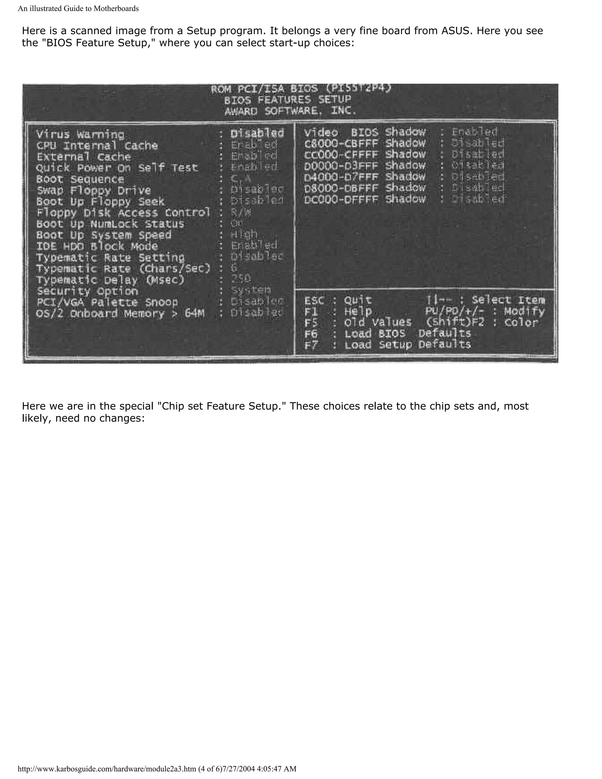
The BIOS Feature Setup
The Feature Setup is the next layer in the CMOS setup. Here you can choose among options like:
q Quick execution of POST (a good thing).
q Choice of boot device EIDE/SCSI. If you have both types of hard drives, which one is to be booted?
q The boot sequence.
q ....
Modifying the boot sequence
You can change the boot sequence from A:, C: to C:, A:. That means, that the PC will not try to boot
from any diskette in the A drive. This will protect you from certain virus attacks from the boot sector.
Also, the boot process will not be blocked by any diskette in the A drive. If you need to boot from A-
drive (for example, if you want to install Windows 98), you have to enter Setup again, and change the
boot sequence to A:, C:. That is no problem.
Power Management
You also use the Setup program to regulate the power management , which is the power saving
features in the motherboard. For example, you can make the CPU shut down after one minute of no
activity. There are plenty of settings available in this area. The power management functions found on
the PC’s motherboard will cooperate with the operating system. Especially Windows 98 is very good at
using the power management.
Password Protection
You can protect the Setup program with a password. This is used widely in schools, where the teachers
do not want the little nerds to make changes in the setup. Please remember the password (write it down
in the motherboard manual). If you forget it you have to remove the battery from the motherboard.
Then all user input to the CMOS is erased - including the password.
[top]
Images from the Setup program
http://www.karbosguide.com/hardware/module2a3.htm (3 of 6)7/27/2004 4:05:47 AM](https://image.slidesharecdn.com/computerhardware-michaelkarbo-121118154249-phpapp01/75/Computer-hardware-michael-karbo-36-2048.jpg)
![An illustrated Guide to Motherboards
q Next page
q Previous page
Learn more [top]
Module 2b. About the boot process and system bus
Read more about I/O buses in module 2c
Read more about the motherboard chip set in module 2d
Read more about RAM in module 2e
Read about EIDE in module 5b
I also recommend two books for further studies. Gunnar Forst: "PC Principals", from MIT is excellent.
Also "The Winn L. Rosch Hardware Bible" from Brady covers the same subjects. Also "PC Intern" from
Abacus is fine.
Links to BIOS information:
http://www.karbosguide.com/hardware/module2a3.htm (5 of 6)7/27/2004 4:05:47 AM](https://image.slidesharecdn.com/computerhardware-michaelkarbo-121118154249-phpapp01/75/Computer-hardware-michael-karbo-38-2048.jpg)
![An illustrated Guide to Motherboards
BIOS Guide
Mr BIOS FAQ
[Main page] [Contact] [Karbo's Dictionary] [The Windows 98 pages]
Copyright (c) 1996-2001 by Michael B. Karbo. www.karbosguide.com.
http://www.karbosguide.com/hardware/module2a3.htm (6 of 6)7/27/2004 4:05:47 AM](https://image.slidesharecdn.com/computerhardware-michaelkarbo-121118154249-phpapp01/75/Computer-hardware-michael-karbo-39-2048.jpg)
![An illustrated Guide to Motherboards
KarbosGuide.com. Module 2a.4.
The system software of hardware
The contents:
q Next page
q Previous page
The BIOS in adapter ROM
[top]
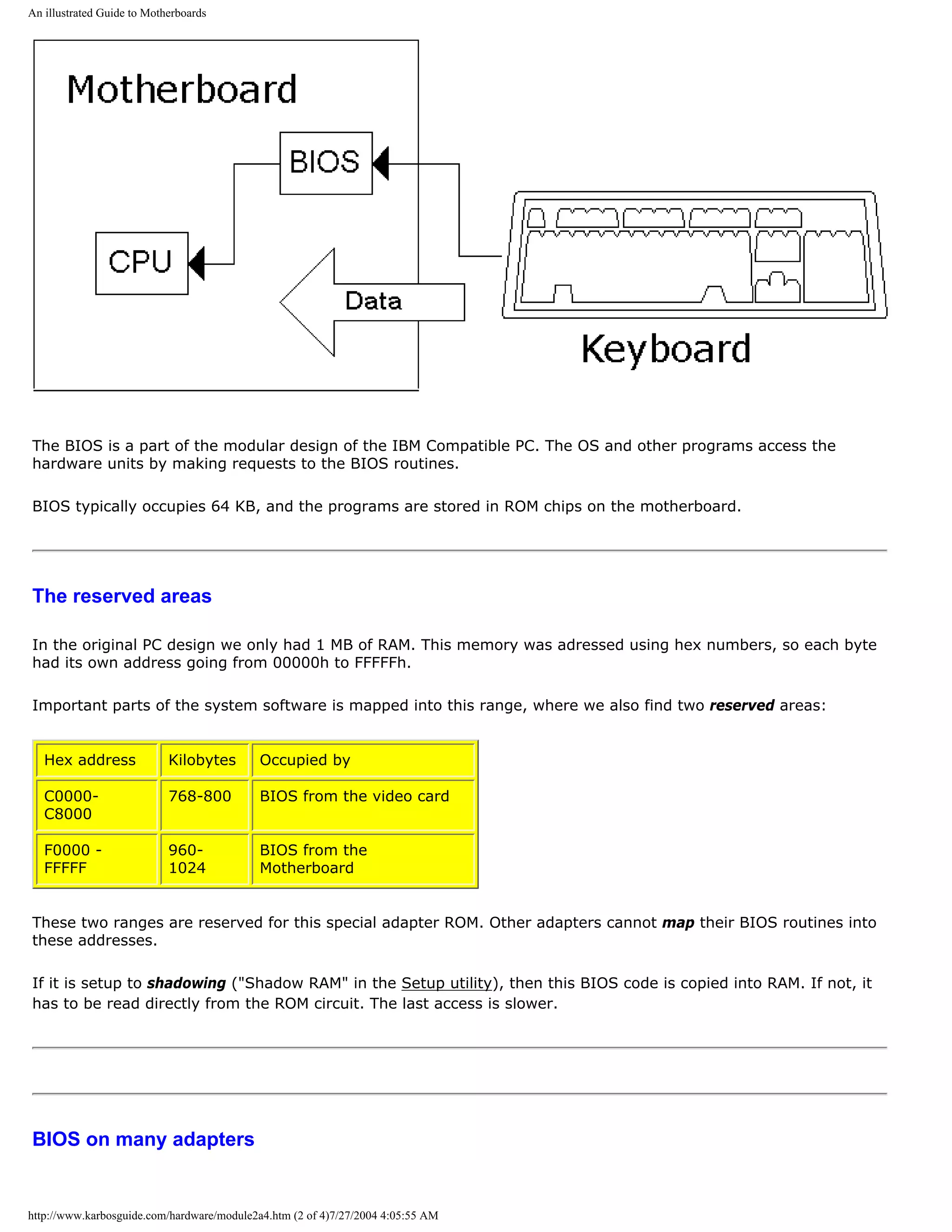
During the start-up process the BIOS programs are read from the ROM circuits. BIOS stands for Basic Input
Output System and it is small program routines which controls specific hardware units.
For instance you have a BIOS routine which reads the keyboard:
http://www.karbosguide.com/hardware/module2a4.htm (1 of 4)7/27/2004 4:05:55 AM](https://image.slidesharecdn.com/computerhardware-michaelkarbo-121118154249-phpapp01/75/Computer-hardware-michael-karbo-40-2048.jpg)
![An illustrated Guide to Motherboards
There are BIOS codes on many adapters (expansion cards). The adapters are external hardware, which are
connected to and “integrated” with the motherboard during the hardware configuration and internalizing.
The adapters hold their own BIOS code making them functional. This BIOS must be included during the
configuration. Therefore, the adapter ROM is read during start-up, and the program code is “woven” together
with other BIOS programs and the CMOS data. It is all written into RAM, where it is ready for the operating
system, as you can see here:
The BIOS routines are not always in use. They can be regarded as basic program layers in the PC, giving it a
simple functionality.
Many programs routinely bypass BIOS. In that case, they "write direct to hardware", as we say. Windows
contains program files, which can be written directly to all kinds of hardware - bypassing BIOS routines. One
example is the COM ports. If you use the BIOS routines connected with them, you can transmit only at max.
9600 baud on the modem. That is insufficient. Therefore, Windows will assume control over the COM port.
BIOS update
BIOS programs can be updated . The modern motherboard has the BIOS instructions in flash ROM, which can be
updated. You can get new BIOS software from your supplier or on the Internet, which can be read onto the
motherboard. The loading is a special process, where you might need to change a jumper switch on the
motherboard. Usually, you do not need to do this, but it is a nice available option.
ATX motherboards [top]
The latest PC electronic standard is called ATX. It consists of a new type motherboard with a specific physical
design like the traditional board (30.5 cm X 19 cm). However the board has been shifted 90 degrees for a better
http://www.karbosguide.com/hardware/module2a4.htm (3 of 4)7/27/2004 4:05:55 AM](https://image.slidesharecdn.com/computerhardware-michaelkarbo-121118154249-phpapp01/75/Computer-hardware-michael-karbo-42-2048.jpg)
![An illustrated Guide to Motherboards
placing of the units.
The I/O connectors COM1, COM2 and LPT, keyboard, mouse and USB are mounted directly on the motherboard.
The ATX board requires specifically designed chassises with an I/O access opening measuring 1¾ by 6¼ inch.
ATX is designed by Intel, but has gained general acceptance.
The ATX motherboard is more ”intelligent” than the ordinary type. In a few years, it will be wide spread. It
includes advanced control facilities, where the BIOS program continually checks the CPU temperature and
voltages, the cooling fans RPM, etc. If over heating occurs, the PC will shut down automatically. The PC can also
be turned on by for example modem signals, since the power supply is controlled by the motherboard. The on/off
button will turn the PC "down" without turning it completely off.
If you want a PC designed for the future, the ATX layout is what you should go for.
q Next page
q Previous page
Learn more [top]
Module 2b. About the boot process and system bus
Read more about I/O buses in module 2c
Read more about the motherboard chip set in module 2d
Read more about RAM in module 2e
Read about EIDE in module 5b
I also recommend two books for further studies. Gunnar Forst: "PC Principals", from MIT is excellent. Also "The
Winn L. Rosch Hardware Bible" from Brady covers the same subjects. Also "PC Intern" from Abacus is fine.
Links to BIOS information:
BIOS Guide
Mr BIOS FAQ
[Main page] [Contact] [Karbo's Dictionary] [The Windows 98 pages]
Copyright (c) 1996-2001 by Michael B. Karbo. www.karbosguide.com.
http://www.karbosguide.com/hardware/module2a4.htm (4 of 4)7/27/2004 4:05:55 AM](https://image.slidesharecdn.com/computerhardware-michaelkarbo-121118154249-phpapp01/75/Computer-hardware-michael-karbo-43-2048.jpg)
![An illustrated Guide to the PC System BUS
KarbosGuide.com. Module 2b1.
About the System Bus
In this module, you can read about the following subjects, which add to our tour of the PC:
q The boot process q Next page
q Data on the motherboard q Previous page
The boot process [top]
The last step in the PC start-up is reading the operating system. The start-up program is instructed to
find the Master Boot Record. This is located in the very first sector on either hard disk (C) or floppy
drive A. From the MBR it reads the boot-strap which points to the location of the startup files of the
Operating System.
By default, the PC will look for a boot sector in floppy drive A. That is why the PC "drops dead" if there is
a different diskette in A drive. If there is no diskette in A drive, the start-up program will search for the
boot sector on hard drive C. When the boot sector is found, a small program segment (boot-strap) is
read from there. The boot-strap then takes over control of the PC. The start-up program has done its
job. Now DOS, Windows , or another operating system takes control.
Read more about boot sectors, etc. in module 6a, which deals with file systems.
Here is an illustration of the start-up process:
http://www.karbosguide.com/hardware/module2b1.htm (1 of 4)7/27/2004 4:05:57 AM](https://image.slidesharecdn.com/computerhardware-michaelkarbo-121118154249-phpapp01/75/Computer-hardware-michael-karbo-44-2048.jpg)
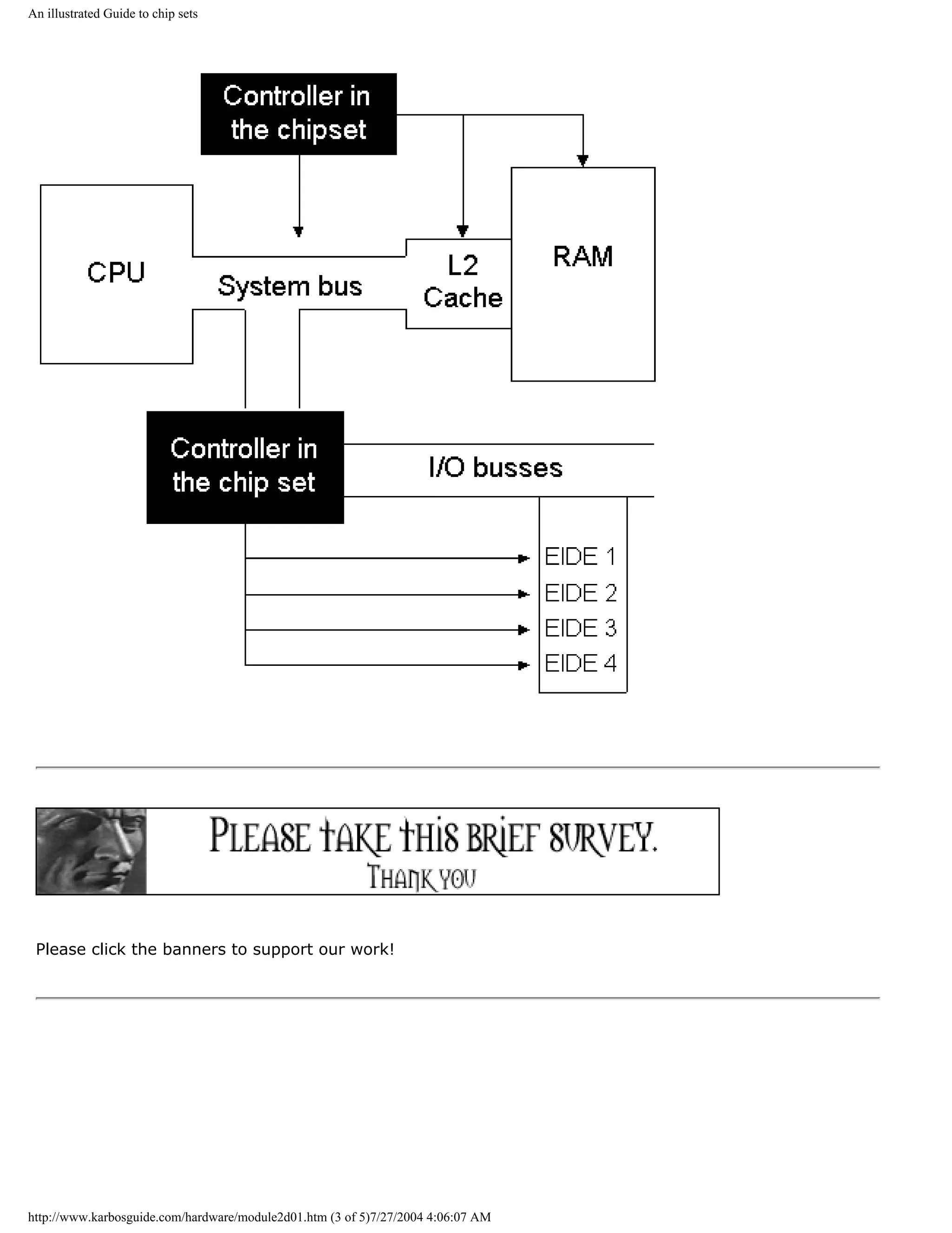
![An illustrated Guide to the PC System BUS
The data flow on the motherboard
[top]
On the motherboard, you will find the CPU, which is the "brain" of the PC and the buses. The buses are
the nerve system of the motherboard. They connect the CPU to all the other components. There are at
least three buses, which you can see below. You can read more about those on the following pages.
The buses are the PC's expressways. They are "wires" on the circuit board, which transmit data between
different components.
One "wire" can move one bit at a time. In the following text, we start from a typical Pentium board. We
will look at buses, chip sets and CPUs. Here is an illustration of some of the motherboard "logic." You
can print it:
http://www.karbosguide.com/hardware/module2b1.htm (2 of 4)7/27/2004 4:05:57 AM](https://image.slidesharecdn.com/computerhardware-michaelkarbo-121118154249-phpapp01/75/Computer-hardware-michael-karbo-45-2048.jpg)
![An illustrated Guide to the PC System BUS
q Next page
q Previous page
Learn more [top]
Read more about the motherboards chip set in module 2d
Read more about RAM in module 2e
[Main page] [Contact] [Karbo's Dictionary] [The Software Guides]
http://www.karbosguide.com/hardware/module2b1.htm (3 of 4)7/27/2004 4:05:57 AM](https://image.slidesharecdn.com/computerhardware-michaelkarbo-121118154249-phpapp01/75/Computer-hardware-michael-karbo-46-2048.jpg)
![An illustrated Guide to the PC System BUS
KarbosGuide.com. Module 2b2.
About the System Bus
In this module, you can read about the following subjects, which add to our tour of the PC:
q PC buses, an intro q Next page
q The system bus q Previous page
q 66 MHz bus
q 100 MHz bus
Introduction to the PC buses
[top]
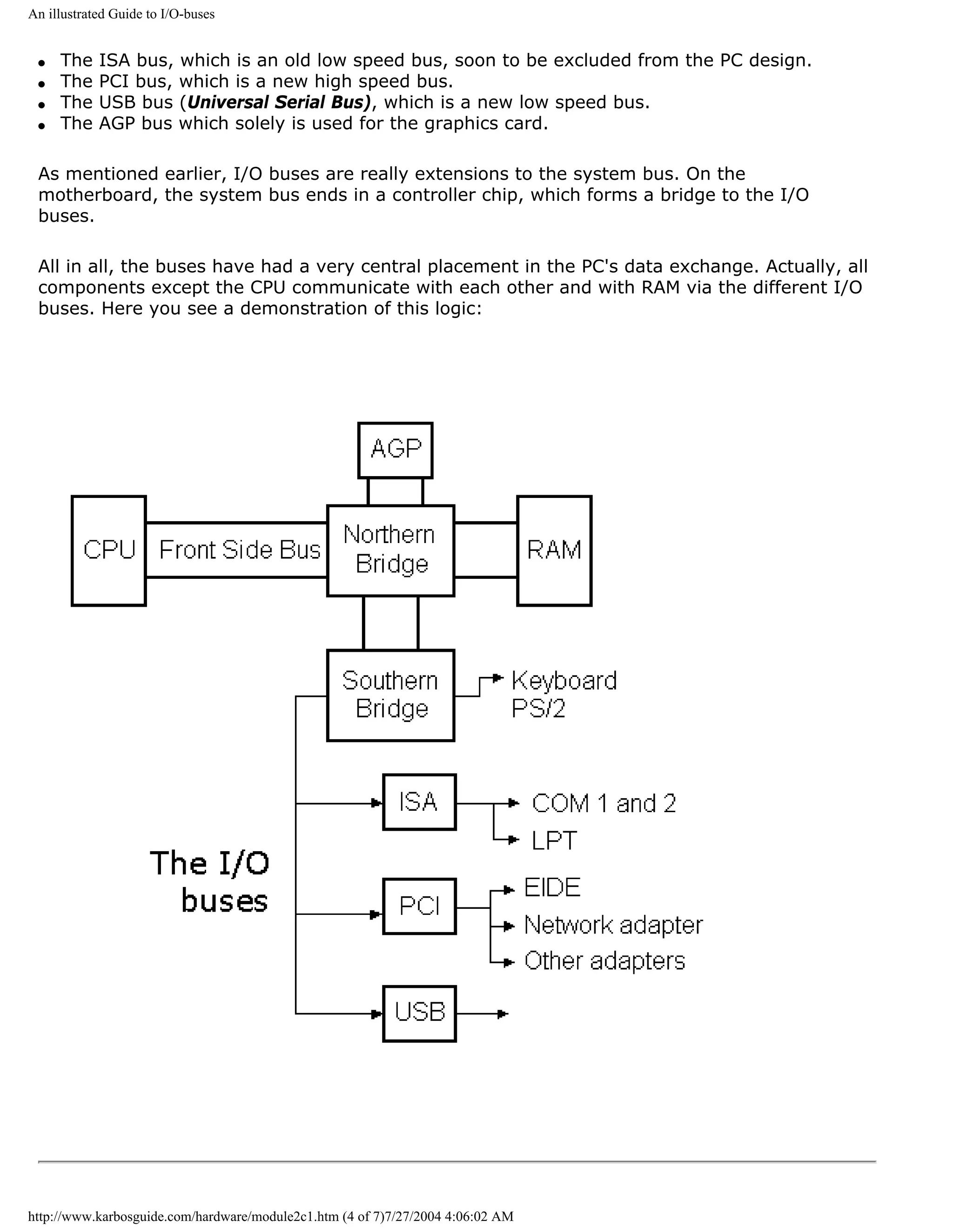
The PC receives and sends its data from and to buses. They can be divided into:
q The system bus, which connects the CPU with RAM
q I/O buses, which connect the CPU with other components.
http://www.karbosguide.com/hardware/module2b2.htm (1 of 6)7/27/2004 4:05:59 AM](https://image.slidesharecdn.com/computerhardware-michaelkarbo-121118154249-phpapp01/75/Computer-hardware-michael-karbo-48-2048.jpg)
![An illustrated Guide to the PC System BUS
The point is, that the system bus is the central bus. Actually, it
connects to the I/O buses, as you can see in this illustration. It is not
completely correct, since the architecture is much more complex, but
it shows the important point, that the I/O-buses usually derive from
the system bus:
You see the central system bus, which connects the CPU with RAM. A bridge connects the I/O
buses with the system bus and on to RAM. The bridge is part of the PC chip set, which will be
covered in module 2c.
3 different I/O buses
[top]
The I/O buses move data. They connect all I/O devices with the CPU and RAM. I/O devices
are those components, which can receive or send data (disk drives, monitor, keyboard, etc. ).
In a modern Pentium driven PC, there are two or three different I/O buses:
q The ISA bus, which is oldest, simplest, and slowest bus.
q The PCI bus, which is the fastest and most powerful bus.
q The USB bus, which is the newest bus. It may in the long run replace the ISA bus.
The three I/O buses will be described later. Here, we will take a closer look at the PC's
http://www.karbosguide.com/hardware/module2b2.htm (2 of 6)7/27/2004 4:05:59 AM](https://image.slidesharecdn.com/computerhardware-michaelkarbo-121118154249-phpapp01/75/Computer-hardware-michael-karbo-49-2048.jpg)
![An illustrated Guide to the PC System BUS
fundamental bus, from which the others are branches from.
The system bus
[top]
The system bus connects the CPU with RAM and maybe a buffer memory (L2-cache). The
system bus is the central bus. Other buses branch off from it.
The system bus is on the motherboard. It is designed to match a specific type of CPU.
Processor technology determines dimensioning of the system bus. At the same time, it has
taken much technological development to speed up "traffic" on the motherboard. The faster
the system bus gets, the faster the remainder of the electronic components must be..
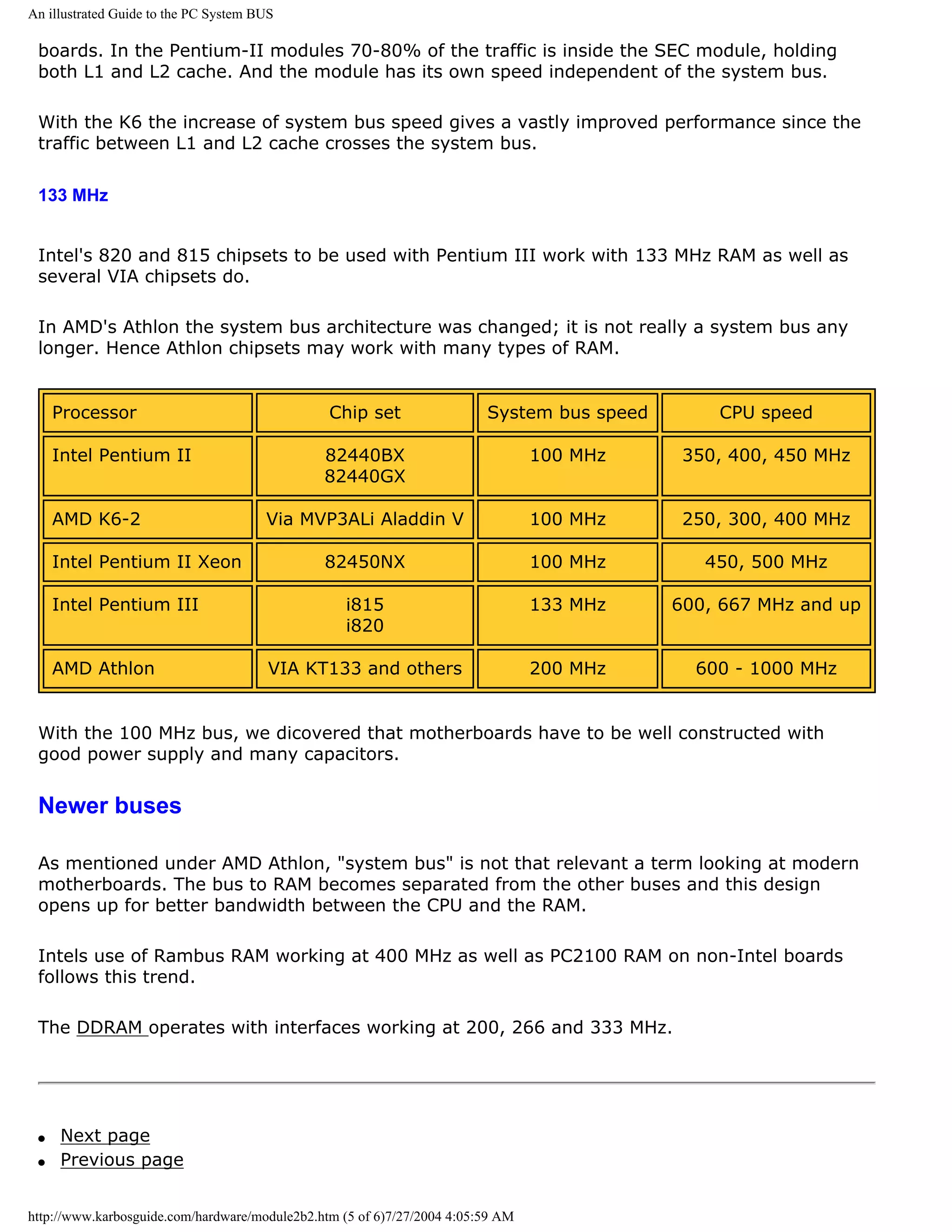
The following three tables show different CPUs and their system buses:
Older CPUs System bus width System bus
speed
8088 8 bit 4.77 MHz
8086 16 bit 8 MHz
80286-12 16 bit 12 MHz
80386SX-16 16 bit 16 MHz
80386DX-25 32 bit 25 MHz
We see, that system bus speed follows the CPU's speed limitation. First at the fourth
generation CPU 80486DX2-50 are doubled clock speeds utilized. That gives the CPU a higher
internal clock frequency. The external clock frequency, used in the system bus, is only half of
the internal frequency:
CPUs in the 80486 family System bus width System bus
speed
80486SX-25 32 bit 25 MHz
80486DX-33 32 bit 33 MHz
80486DX2-50 32 bit 25 MHz
80486DX-50 32 bit 50 MHz
http://www.karbosguide.com/hardware/module2b2.htm (3 of 6)7/27/2004 4:05:59 AM](https://image.slidesharecdn.com/computerhardware-michaelkarbo-121118154249-phpapp01/75/Computer-hardware-michael-karbo-50-2048.jpg)
![An illustrated Guide to the PC System BUS
80486DX2-66 32 bit 33 MHz
80486DX4-100 32 bit 40 MHz
5X86-133 32 bit 33 MHz
66 MHz bus
[top]
For a long time all Pentium based computers ran at 60 or 66 MHz on the system bus, which is
64 bit wide:
CPUs in the System bus width System bus
Pentium family speed
Intel P60 64 bit 60 MHz
Intel P100 64 bit 66 MHz
Cyrix 6X86 P133+ 64 bit 55 MHz
AMD K5-133 64 bit 66 MHz
Intel P150 64 bit 60 MHz
Intel P166 64 bit 66 MHz
Cyrix 6X86 P166+ 64 bit 66 MHz
Pentium Pro 200 64 bit 66 MHz
Cyrix 6X86 P200+ 64 bit 75 MHz
Pentium II 64 bit 66 MHz
100 MHz bus
The speed of the system bus has increased in 1998. Using PC100 SDRAM a speed of 100 MHz
is well proven and the use of RDRAM will give us much higher speeds.
However the rise from 66 MHz to 100 MHz has the greatest impact on Socket 7 CPUs and
http://www.karbosguide.com/hardware/module2b2.htm (4 of 6)7/27/2004 4:05:59 AM](https://image.slidesharecdn.com/computerhardware-michaelkarbo-121118154249-phpapp01/75/Computer-hardware-michael-karbo-51-2048.jpg)
![An illustrated Guide to the PC System BUS
Learn more [top]
Read more about the motherboards chip set in module 2d
Read more about RAM in module 2e
[Main page] [Contact] [Karbo's Dictionary] [The Software Guides]
Copyright (c) 1996-2001 by Michael B. Karbo. www.karbosguide.com.
http://www.karbosguide.com/hardware/module2b2.htm (6 of 6)7/27/2004 4:05:59 AM](https://image.slidesharecdn.com/computerhardware-michaelkarbo-121118154249-phpapp01/75/Computer-hardware-michael-karbo-53-2048.jpg)
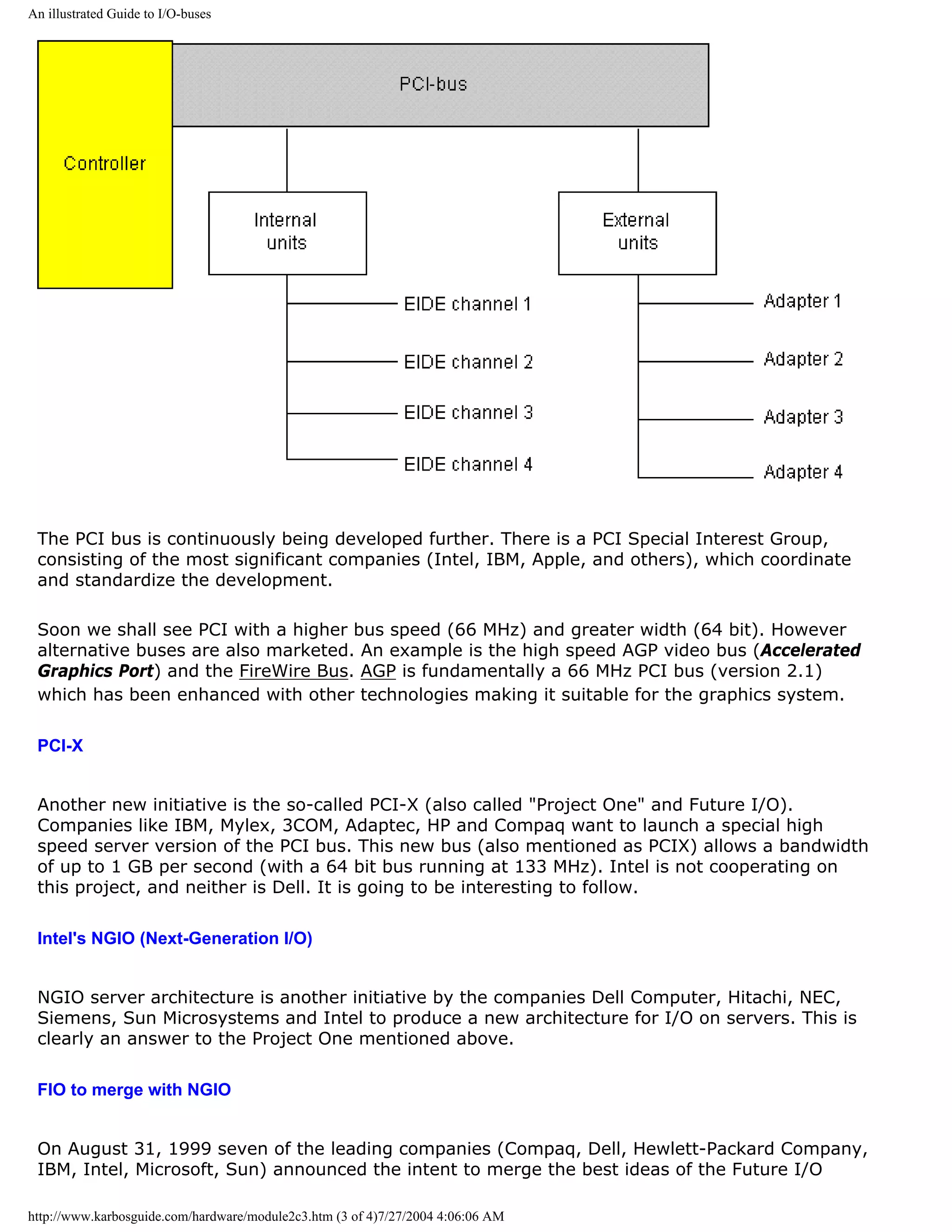
![An illustrated Guide to I/O-buses
Introduction to the I/O buses [top]
We have seen before, that the PC's buses are the fundamental data
"highways" on the system board. The "first" bus is the system bus,
which connects the CPU with RAM. In older designs it was a local bus.
In newer designs this bus is called the front side bus (FSB).
The typical local bus has a speed and width depending on the type
CPU installed on the motherboard. Typically, the system bus will be
64 bits wide and run at 66, 100 or 133 MHz. These high speeds create
electrical noises and other problems. Therefore, the speed must be
reduced for data reaching the expansion cards and other more
peripheral components.
Very few expansion cards can operate at more than 40 MHz. Then the electronics shut down.
The chips can just not react faster. Therefore, the PC has additional buses.
Originally only one bus
However, the first PCs had only one bus, which was common for the CPU, RAM and I/O
components:
The older first and second generation CPUs ran at relatively low clock frequencies, and all
system components could keep up with those speeds.
RAM on adapters
Among other things, that allowed additional RAM to be installed in expansion slots in the PC,
http://www.karbosguide.com/hardware/module2c1.htm (2 of 7)7/27/2004 4:06:02 AM](https://image.slidesharecdn.com/computerhardware-michaelkarbo-121118154249-phpapp01/75/Computer-hardware-michael-karbo-55-2048.jpg)
![An illustrated Guide to I/O-buses
by installing an adapter in a vacant expansion slot. An adapter, where RAM was mounted:
This setup would be unthinkable today. However it is truely a local bus. All units are united
on one bus using the same clock.
First in 1987, Compaq figured out how to separate system bus from I/O bus, so they could
run at different speeds. This multi-bus architecture has been industry standard ever since.
Modern PCs also have more than one I/O bus.
What does an I/O bus do?
[top]
I/O buses connect the CPU to all other components, except RAM. Data are moved on the
buses from one component to another, and data from other components to the CPU and RAM.
The I/O buses differ from the system bus in speed. Their speed will always be lower than the
system bus speed. Over the years, different I/O buses have been developed. On modern PCs,
you will usually find four buses:
http://www.karbosguide.com/hardware/module2c1.htm (3 of 7)7/27/2004 4:06:02 AM](https://image.slidesharecdn.com/computerhardware-michaelkarbo-121118154249-phpapp01/75/Computer-hardware-michael-karbo-56-2048.jpg)
![An illustrated Guide to I/O-buses
The physical aspects of the I/O buses
[top]
Physically, the I/O bus consists of tracks on the printed circuit board. These tracks are used
as:
q Data tracks, which each can move one bit at a time
q Address tracks, which identify where data should be sent to
q Other tracks for clock ticks, voltage, verification signals, etc.
When data are sent on the bus, they must be supplied with a receiver. Therefore, each device
on the bus has an address. Similarly, the RAM is divided in sections, each having its address.
Prior to sending data, a number is sent on the address track, to identify where the data
should be sent to.
The bus width
The number of data tracks determine the data transfer capacity. The ISA bus is slow, partly
because it only has 16 data tracks. The modern PCs send 32 bits per clock tick. On the ISA
bus, 32 bits must be divided in two packages of 16 bits. This delays the data transfer.
Another I/O bus concept is wait states.
Wait states
Wait states are small pauses. If an ISA adapter cannot keep up with the incoming data flow,
its controller sends wait states to the CPU. Those are signals to the CPU to "hold on for a
sec." A wait state is a wasted clock tick. The CPU skips a clock tick, when not occupied. Thus
the old and slow ISA adapter can significantly reduce the operating speed of a modern
computer.
Another aspect is the IRQ signals, which the components use to attract attention from the
CPU. That and the concepts DMA and bus mastering, are described in module 5, which deals
with adapters.
Technical and historical background for the I/
O buses [top]
In modern PCs you only find the PCI and ISA buses (besides USB, which we do not know
http://www.karbosguide.com/hardware/module2c1.htm (5 of 7)7/27/2004 4:06:02 AM](https://image.slidesharecdn.com/computerhardware-michaelkarbo-121118154249-phpapp01/75/Computer-hardware-michael-karbo-58-2048.jpg)
![An illustrated Guide to I/O-buses
much about yet). But, over the years, there have been other buses. Here is a diagram of the
various I/O buses. Then comes a more detailed description of each of the buses:
Bus Max. throughput
Year Bus width Bus speed
(theoretical)
Synchronous with CPU:
PC and XT 1980-82 8 bit 4-6 MBps
4.77 - 6 MHz
ISA (AT) 1984 16 bit Synchronous: 8 MBps
Simple bus. 8-10 MHz
MCA. Advanced, 1987 32 bit Asynchronous: 40 MBps
intelligent bus by IBM. 10.33 MHz
EISA. 1988 32 bit Synchronous: 32 MBps
Bus for servers. max. 8 MHz
VL. High speed bus, 1993 32 bit Synchronous: 100-160
used in 486s. 33-50 MHz MBps
PCI. Intelligent, 1993 32 bit Asynchronous: 132 MBps
advanced high speed 33 MHz
bus.
USB. Modern, simple, 1996 Serial 1.2 MBps
and intelligent bus.
FireWire (IEEE1394). 1999 Serial 80 MBps
High-speed I/O bus for
storage, video etc.
USB 2.0 2001 Serial 12-40 MBps
SCSI is another type of bus.
q Next page
q Previous page
Learn more [top]
5c about the modern I/O bus called USB.
http://www.karbosguide.com/hardware/module2c1.htm (6 of 7)7/27/2004 4:06:02 AM](https://image.slidesharecdn.com/computerhardware-michaelkarbo-121118154249-phpapp01/75/Computer-hardware-michael-karbo-59-2048.jpg)
![An illustrated Guide to I/O-buses
Read module 5b about AGP and module 5c about Firewire.
Read more about chip sets on the motherboard in module 2d
Read about RAM in module 2e
Read Module 4b about hard disks.
Read Module 4c about optical media (CDROM and DVD).
Read Module 4d about super diskette and MO drives.
Read module 5a about expansion cards, where we evaluate the I/O buses from the port side.
Read module 7a about monitors, and 7b on graphics card.
Read module 7c about sound cards, and 7d on digital sound and music.
[Main page] [Contact] [Karbo's Dictionary] [The Software Guides]
Copyright (c) 1996-2001 by Michael B. Karbo. www.karbosguide.com.
http://www.karbosguide.com/hardware/module2c1.htm (7 of 7)7/27/2004 4:06:02 AM](https://image.slidesharecdn.com/computerhardware-michaelkarbo-121118154249-phpapp01/75/Computer-hardware-michael-karbo-60-2048.jpg)
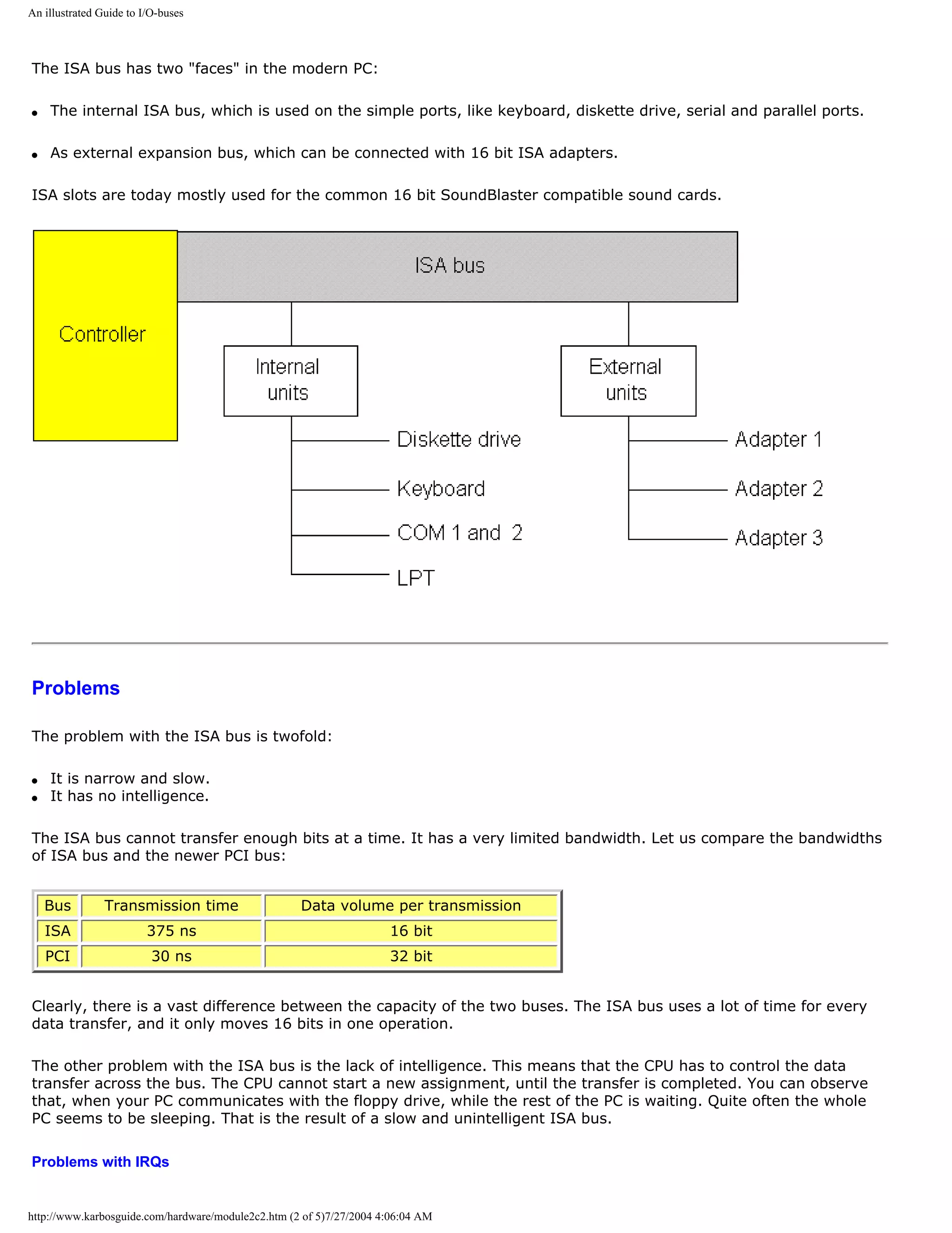
![An illustrated Guide to I/O-buses
The ISA bus can be a tease, when you install new expansion cards (for example a sound card). Many of these
problems derive from the tuning of IRQ and DMA, which must be done manually on the old ISA bus.
Every component occupies a specific IRQ and possibly a DMA channel. That can create conflict with existing
components. Read module 5 about expansion cards and these problems.
The ISA bus is out
As described, the ISA bus is quite outdated and should not be used in modern pcs. There is a good chance, that
this "outdated legacy technology" (quoting Intel) will disappear completely.
The USB bus is the technology that will replace it. It has taken many years to get this working and accepted, but it
works now.
Intel's chip set 810 was the first not to include ISA support.
MCA, EISA and VLB [top]
In the 80s, a demand developed for buses more powerful than the ISA. IBM developed the
MCA bus and Compaq and others responded with the EISA bus. None of those were Please support our
particularly fast, and they never became particularly successful outside the server market. sponsor.
MCA
IBM's top of the line bus from 1987 is named Micro Channel Architecture. The MCA bus was a masterpiece, unifying
the best bus technology from the mainframe design with the demands from the PC. However, contrary to the ISA
bus, MCA is patented, and IBM demanded high royalty fees, when other PC manufacturers wanted to use it. Thus
the bus never became a great success, despite its advanced design. It ended up being a classic example of poor
marketing strategy.
The MCA bus is 32 bit wide and "intelligent." The cards configure themselves with respect to IRQ. Thus, they can
be installed without adjustments of jumper switches or other features. It works constantly at 10.33 MHz,
asynchronous with the system bus.
The MCA bus is also relatively fast with transfer rates of up to 40 MBps in 32 bit mode at 10.33 MHz. MCA requires
special adapters. There have never been too many adapters developed, since this bus is by and large used only in
IBM's own PCs.
EISA
EISA is a bus from 1988-89. It is designed by the "Gang of Nine:" the companies AST, Compaq, Epson, Hewlett-
Packard, NEC, Olivetti, Tandy, Wyse and Zenith. It came in response to IBM's patented MCA bus.
EISA is built on the ISA bus; the connector has the same dimensions and old ISA cards fit into the slots. To keep
this compatibility, the EISA bus works at maximum 8 MHz. Like ISA, the bus bus is synchronous with the CPU at a
clock frequency reduced to a fraction of the system bus clock frequency.
http://www.karbosguide.com/hardware/module2c2.htm (3 of 5)7/27/2004 4:06:04 AM](https://image.slidesharecdn.com/computerhardware-michaelkarbo-121118154249-phpapp01/75/Computer-hardware-michael-karbo-63-2048.jpg)
![An illustrated Guide to I/O-buses
EISA is compatible with ISA in the sense that ISA adapters can be installed in EISA slots. The EISA adapters hold a
second level of connectors in the button of the slot.
However, EISA is much more intelligent than ISA. It has bus mastering, divided interrupts and self configuration. It
is 32 bit wide, and with it's compressed transfers and BURST modegives a highly improved performance.
But, like the MCA, it did not have great success. The EISA bus is still used in some servers.
Vesa Local Bus
This Bus called VLB for short. It is an inexpensive and simple technology. This bus only achieved status as an
interim phenomenon (in 1993-94). VLB was widely used on 486 motherboards, where the system bus runs at 33
MHz. VLB runs directly with the system bus. Therefore, data transfer is at CPU speed, synchronous and in width.
The problem with VLB was compatibility. Adapters and system system boards would not always work together.
Vesa is an organization with about 120 members, mostly monitor and graphics card manufacturers. Therefore,
most VLB cards were video cards.
q Next page
q Previous page
Learn more [top]
Read module 5c about the modern I/O bus called USB.
Read module 5a about expansion cards, where we evaluate the I/O buses from the port side.
Read module 5b about AGP and module 5c about Firewire
Read more about chip sets on the motherboard in module 2d.
Read more about RAM in module 2e.
Read Module 4b about hard disks.
Read Module 4c about optical media (CDROM and DVD).
Read Module 4d about super diskette and MO drives.
Read module 7a about monitors, and 7b on graphics card.
Read module 7c about sound cards, and 7d on digital sound and music.
[Main page] [Contact] [Karbo's Dictionary] [The Software Guides]
http://www.karbosguide.com/hardware/module2c2.htm (4 of 5)7/27/2004 4:06:04 AM](https://image.slidesharecdn.com/computerhardware-michaelkarbo-121118154249-phpapp01/75/Computer-hardware-michael-karbo-64-2048.jpg)
![An illustrated Guide to I/O-buses
KarbosGuide.com. Module 2c.3
About the PCI bus
The contents:
q Introducing the PCI bus q Next page
q The internal and external face. q Previous page
q The future design
q NGIO
Introducing the PCI bus
[top]
The PCI is the high speed bus of the 1990s. PCI stands for Peripheral
Component Interconnect. This bus is made by Intel. It is used today in Please support our
all PCs and other computers for connecting adapters, such as network- sponsor.
controllers, graphics cards, sound cards etc.
Some graphics cards however use the AGP-bus, which is a separate bus only intended for
graphics.
http://www.karbosguide.com/hardware/module2c3.htm (1 of 4)7/27/2004 4:06:06 AM](https://image.slidesharecdn.com/computerhardware-michaelkarbo-121118154249-phpapp01/75/Computer-hardware-michael-karbo-66-2048.jpg)
![An illustrated Guide to I/O-buses
(FIO) and Next Generation I/O (NGIO). The new open input/output architecture will find use in
servers. The bandwidth will be up to 6 GByte/sec.
The new standard NGIO will hardly go into production before 2001.
q Next page
q Previous page
Learn more [top]
Read module 5a about expansion cards, where we evaluate the I/O buses from the port side.
Read module 5b about AGP and module 5c about Firewire.
Read about chip sets on the motherboard in module 2d
Read more about RAM in module 2e
Read Module 4b about hard disks.
Read Module 4c about optical media (CDROM and DVD).
Read module 7a about monitors, and 7b on graphics card.
Read module 7c about sound cards, and 7d on digital sound and music.
[Main page] [Contact] [Karbo's Dictionary] [The Software Guides]
Copyright (c) 1996-2001 by Michael B. Karbo. www.karbosguide.com.
http://www.karbosguide.com/hardware/module2c3.htm (4 of 4)7/27/2004 4:06:06 AM](https://image.slidesharecdn.com/computerhardware-michaelkarbo-121118154249-phpapp01/75/Computer-hardware-michael-karbo-69-2048.jpg)
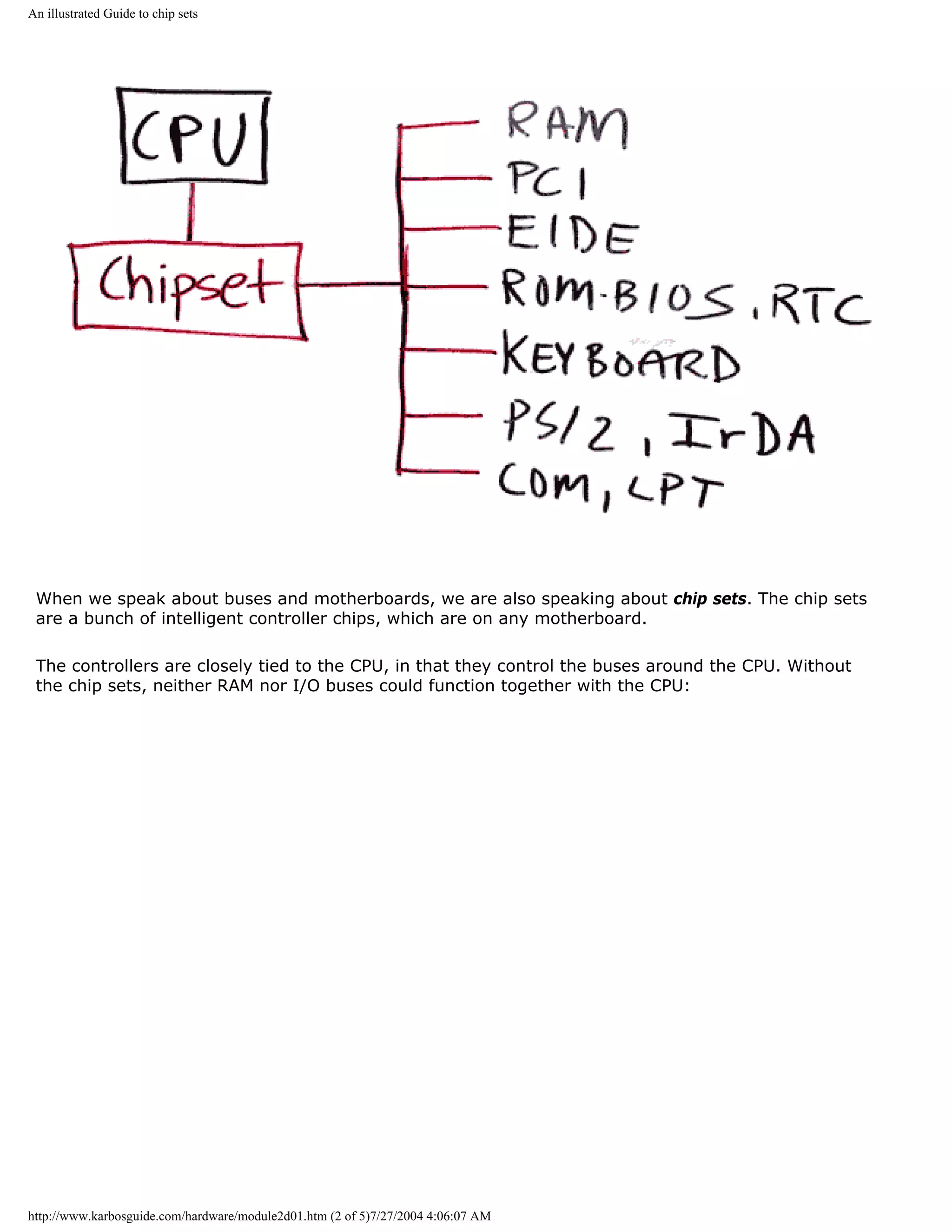
![An illustrated Guide to chip sets
Please click the banners to support our work!
KarbosGuide.com. Module 2d.01
On chip sets
Module 2d describes what chip sets are, and how they function on the motherboards. This module is
subdivided into the following pages:
1: What is a chip set? q Next page
2: The first chip sets for the Pentium boards q Previous
3: Non-Intel chip sets (mostly for Super 7 boards) page
4:
Chip sets for Intel P6 processors
5:
6: More chip sets for Intel P6 processors
7: Intel's i810 "Whitney"
8: Intel's i820 "Camino"
Intel's i815 "Solano"
I recommend that you read all the pages one by one. Just follow the links "Next page" to get
through the textbook. I hope you find the information useful!
What is a chip set?
[top]
The chip set is very important to the modern PC and its performance. Many technologies meet on
the motherboard and are "glued" together via these controllers, which we call the "chip set".
http://www.karbosguide.com/hardware/module2d01.htm (1 of 5)7/27/2004 4:06:07 AM](https://image.slidesharecdn.com/computerhardware-michaelkarbo-121118154249-phpapp01/75/Computer-hardware-michael-karbo-70-2048.jpg)
![An illustrated Guide to chip sets
New technologies - new chip set [top]
Please support our
sponsor.
Therefore, the chip sets are quite central components on the motherboards. When new technological
features are introduced (and this happens continuously) they are often accompanied by new chip
sets. The new chip sets often enable:
q Higher speed on one or more buses
q Utilization of new facilities (new RAM types, new buses, improved EIDE, etc.)
The vendors
There are several suppliers of chip sets for the motherboard:
q Intel
q SIS
q Opti
q Via
q ALi
Intel has hitherto been the leader in supplying chip sets to the Pentium motherboard. Therefore, let
us just mention their chip sets, which have astronomical names.
The Neptune chip set (82434NX) was introduced in June 1994. It replaced the Mercury set
(82434LX). In both chip sets, there were problems with the PCI bus. In January 1995 Intel
introduced the first Triton, where everything worked. This chip set supports some new features: it
supports EDO RAM, and it offers bus master integrated EIDE control and NSP (Native Signal
Processing - one of the many new creations, which was soon forgotten).
However, the following chip sets were of much higher quality, and within very few years they lead to
several new generations of chip sets, each of them more powerful and offering great new features.
q Next page
q Previous page
Learn more [top]
If you want to read more about these and other chip sets, look for the excellent web site Toms
Hardware Guide. Here, you will find all about these subjects.
http://www.karbosguide.com/hardware/module2d01.htm (4 of 5)7/27/2004 4:06:07 AM](https://image.slidesharecdn.com/computerhardware-michaelkarbo-121118154249-phpapp01/75/Computer-hardware-michael-karbo-73-2048.jpg)
![An illustrated Guide to chip sets
Read more about RAM in module 2e
Read about the Pentium in module 3c
Read about the Pentium II's etc. in module 3e
[Main page] [Contact] [Karbo's Dictionary] [The Software Guides]
Copyright (c) 1996-2001 by Michael B. Karbo. KarbosGuide.com
http://www.karbosguide.com/hardware/module2d01.htm (5 of 5)7/27/2004 4:06:07 AM](https://image.slidesharecdn.com/computerhardware-michaelkarbo-121118154249-phpapp01/75/Computer-hardware-michael-karbo-74-2048.jpg)
![An illustrated Guide to chip sets
KarbosGuide.com. Module 2d.02
The first chip sets for the Pentium boards
The contents:
q Triton first and second q Next page
q A bridge to the I/O system q Previous page
q USB and EIDE
q The differences between HX and VX
q The TX chip set
Triton first and second [top]
The interest in chip sets and their performance started in late 1995, when the Pentium
processor became more popular. The Triton controllers were the first chip sets in this trend.
82430FX from late 1995 was Intel's next chip set and the first Triton. In February 1996 the
second generation of Triton arrived. Two new chip sets were introduced: The 82430VX and
82430HX. The last (HX) was the fastest one.
VX and HX
The two sets were similar, yet different. 430HX consisted of two chips. It was designed for
the more professional PCs. 430VX consisted of four chips, but the cost was slightly lower than
HX. It was aimed at the home use PC market. Let us look at the contents of each chip set:
http://www.karbosguide.com/hardware/module2d02.htm (1 of 7)7/27/2004 4:06:10 AM](https://image.slidesharecdn.com/computerhardware-michaelkarbo-121118154249-phpapp01/75/Computer-hardware-michael-karbo-75-2048.jpg)
![An illustrated Guide to chip sets
Chip set Contents
82430HX 82439HX System Controller (TXC)
+ 82371SB PCI ISA IDE Accelerator
82430VX 82437VX System Controller (TVX)
+ two 82438VX Data Path Units (TDX)
+ 82371SB PCI ISA IDE Accelerator
Common to both chip sets is 82371SB, which is a "PCI ISA IDE accelerator chip". It is also
called PIIX3, which some may recognize from the Windows 95 device driver, which comes
with the ASUS T2P4 board.
A bridge to the I/O system [top]
Please support our
sponsor.
The chip makes a bridge between the CPU, ISA and PCI bus. The news was, that it permitted
concurrent activity in all three locations, thus a new form of multitasking. This is significant
for daily use. All data exchange to and from I/O units cross this intersection, which now has
achieved greater width:
.
http://www.karbosguide.com/hardware/module2d02.htm (2 of 7)7/27/2004 4:06:10 AM](https://image.slidesharecdn.com/computerhardware-michaelkarbo-121118154249-phpapp01/75/Computer-hardware-michael-karbo-76-2048.jpg)
![An illustrated Guide to chip sets
US2 and EIDE
[top]
New in the chip was also the host function for USB. It is the Universal Serial Bus, which was
not much use at this time. Finally, the chip included a EIDE Bus Master control. In short that
means, that EIDE components like hard disks, to some extent can deliver their data directly
to RAM without taking up CPU time.
Above, you see the 82371SB chip and below, again, its placement relative to CPU and buses:
http://www.karbosguide.com/hardware/module2d02.htm (3 of 7)7/27/2004 4:06:10 AM](https://image.slidesharecdn.com/computerhardware-michaelkarbo-121118154249-phpapp01/75/Computer-hardware-michael-karbo-77-2048.jpg)
![An illustrated Guide to chip sets
Please click the banners to support our work!
The differences between HX and VX
[top]
It was generally accepted, that the HX set yielded the best performance of the two chip sets
described. But the VX set had two other facilities to offer: Capability for SMBA (Shared
Memory Buffer Architecture). That means among other things, that you can integrate the
http://www.karbosguide.com/hardware/module2d02.htm (4 of 7)7/27/2004 4:06:10 AM](https://image.slidesharecdn.com/computerhardware-michaelkarbo-121118154249-phpapp01/75/Computer-hardware-michael-karbo-78-2048.jpg)
![An illustrated Guide to chip sets
video card on the motherboard with 1 or 2 MB standard RAM, from the working RAM. A
technology, which is used only in the lowest cost PCs, and which soon was abandoned.
Also, the VX set also supported the fast RAM type SD-RAM. HX did not. The VX set could
control up to 128 MB RAM, but it could not cache above 64 MB RAM.
HX controlled 512 MB RAM and was the only Intel Pentium chip set to cache above 64 MB
RAM.
The VX and HX chip sets are both out. They were replaced by the TX chip set, which was the
last Intel chip set for Socket 7 mounted CPUs. Today Ali and VIA produces chip sets for
Socket 7 motherboards.
Intel TX chip set [top]
Please support our
sponsor.
The last chip set to Pentium processors were named 82430TX, which supports two new hot
technologies:
q SD-RAM
q Ultra DMA
Ultra DMA was also called ATA/33, and it is a standard for harddisk interface, which permits
EIDE hard disks to transfer at up to 33 MBps.
This improved EIDE standard is mostly marketed under the name Ultra DMA. Tests show that
Ultra DMA results in a speed increase of 25-75 percent over the traditional EIDE PIO mode 4.
Ultra DMA is the new EIDE standard and has been vastly enhanced since this chip set.
The controllers in the TX chip set
Chip set Chips included
82430TX 82439TX System Controller (TXC)
82371AB PCI ISA IDE Accelerator
The TX set is an update and improvement of the VX set. Relative to this, the TX firstly
http://www.karbosguide.com/hardware/module2d02.htm (5 of 7)7/27/2004 4:06:10 AM](https://image.slidesharecdn.com/computerhardware-michaelkarbo-121118154249-phpapp01/75/Computer-hardware-michael-karbo-79-2048.jpg)
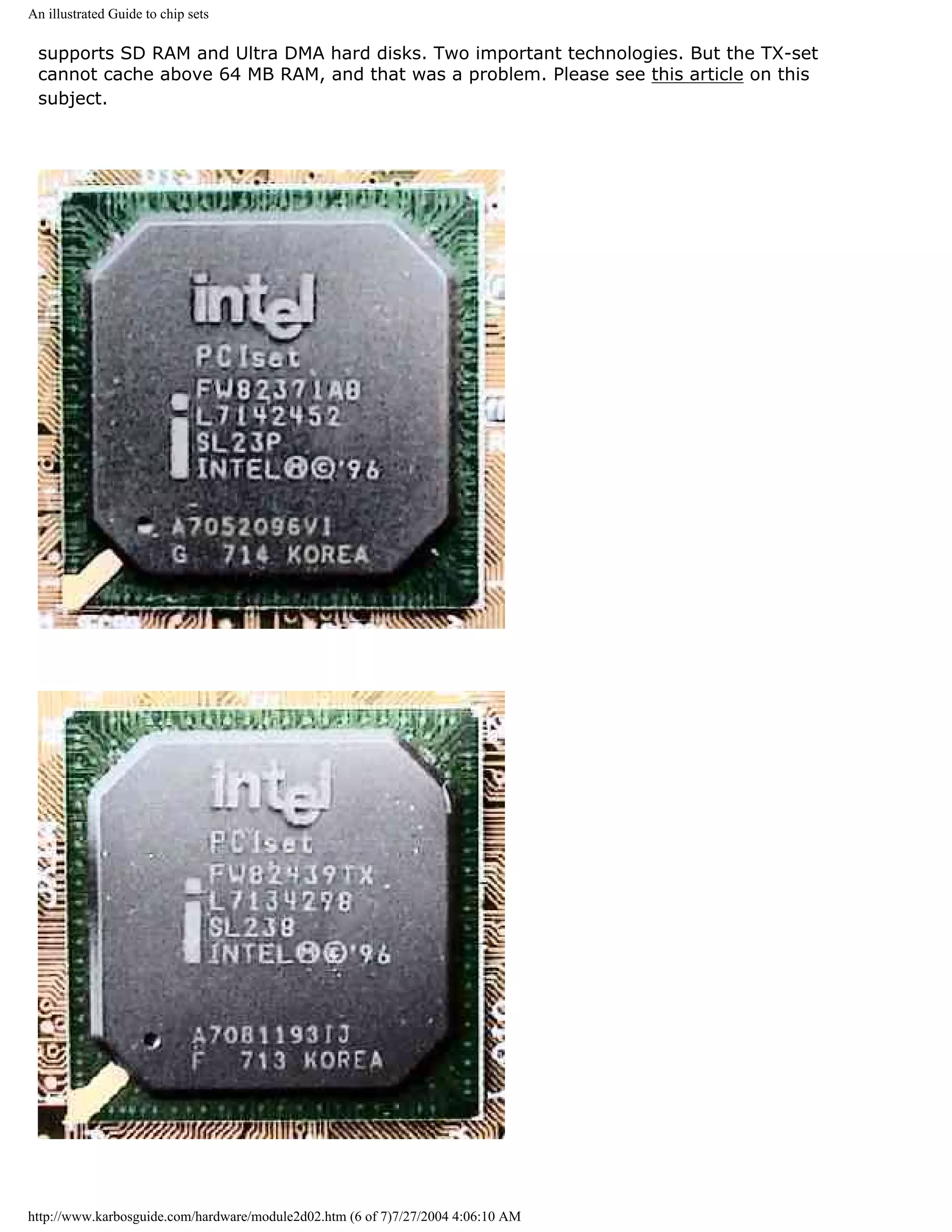
![An illustrated Guide to chip sets
Photos taken with Canon Powershot 600
The TX chip set was Intel's last and final set for Socket 7 motherboards. After that VIA and
ALi took over and continued this work.
q Next page
q Previous page
Learn more [top]
Read more about RAM in module 2e
Read about the Pentium in module 3c
Read about the Pentium II's etc. in module 3e
[Main page] [Contact] [Karbo's Dictionary] [The Software Guides]
Copyright (c) 1996-2001 by Michael B. Karbo. KarbosGuide.com
http://www.karbosguide.com/hardware/module2d02.htm (7 of 7)7/27/2004 4:06:10 AM](https://image.slidesharecdn.com/computerhardware-michaelkarbo-121118154249-phpapp01/75/Computer-hardware-michael-karbo-81-2048.jpg)
![An easy-read and illustrated Guide to SCSI, IEE1394 FireWire and USB.
Please click the banners to support our work!
KarbosGuide.com. Module 5c2a.
About USB
The contents:
q Next page
q Previous page
q What is USB?
q After a slow start ..
On the following page:
q Next page: The USB hub
q Next module: IEEE1394 FireWire
q Device Bay
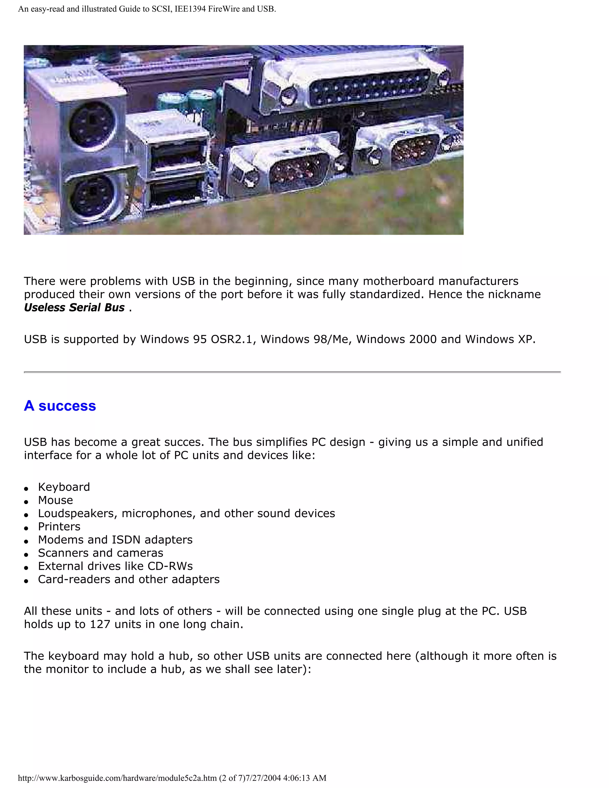
What is USB? [top]
Please support our
sponsor.
USB stands for Universal Serial Bus. It is a cheap and rather slow I/O bus, running at 12 Mbit/
sec.
It can be compared to the FireWire bus, which however is a lot speedier.
USB is an open and royalty-free specification. Units can be plugged and unplugged on the fly
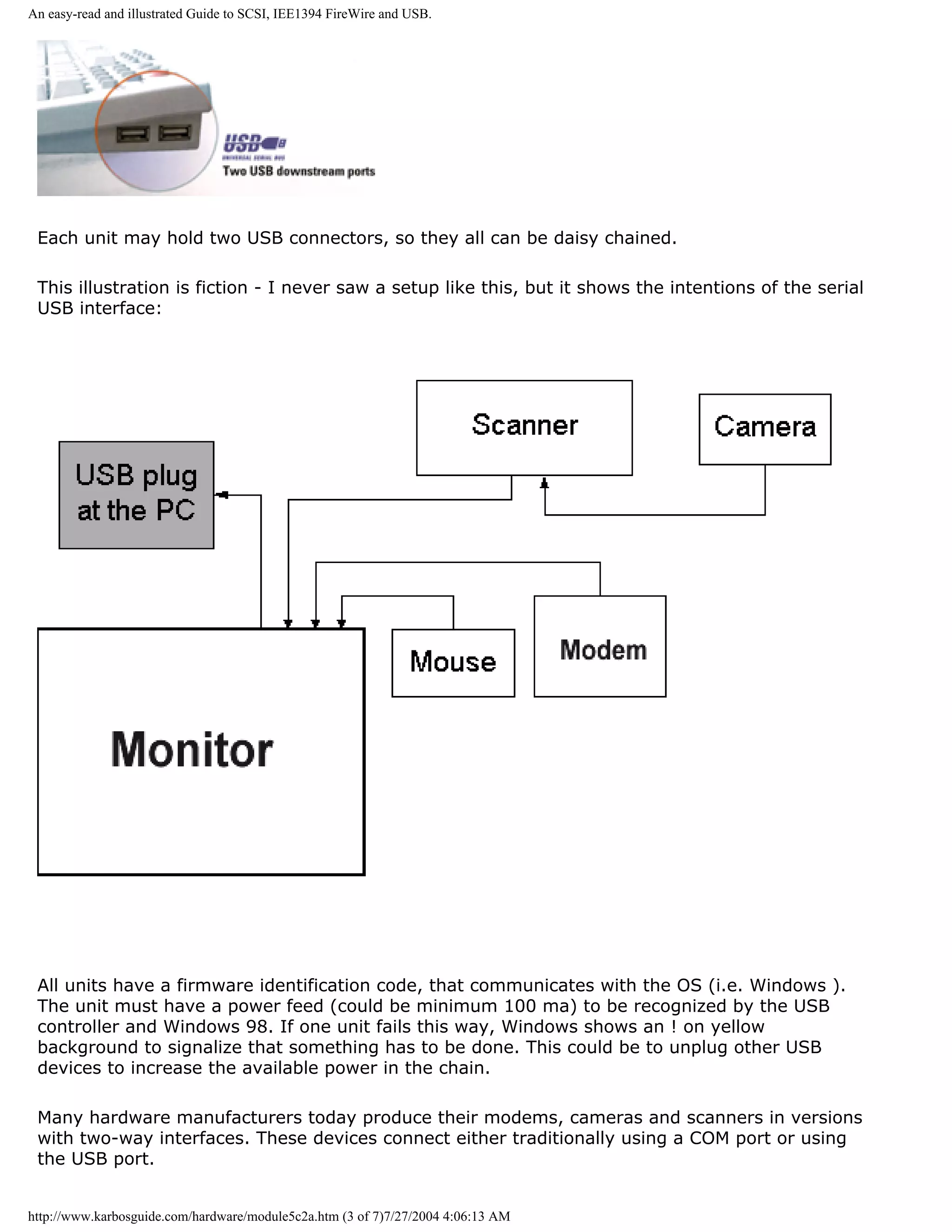
very easily. Here you see the plugs, the two small ones, number two from the left:
http://www.karbosguide.com/hardware/module5c2a.htm (1 of 7)7/27/2004 4:06:13 AM](https://image.slidesharecdn.com/computerhardware-michaelkarbo-121118154249-phpapp01/75/Computer-hardware-michael-karbo-83-2048.jpg)
![An easy-read and illustrated Guide to SCSI, IEE1394 FireWire and USB.
After a slow start ... [top]
Please support our
sponsor.
Personally I always believed, that USB a´´had to become a great renovation of the PC design.
However, things were moving very slowly in the beginning.
Bigger companies like Swiss Logitech (producing the best mice and trackballs available, at least
to my opinion) moved very slowly into USB. This probably has been due to serious concern
over the correct technical implementations. The COM, PS/2, and LPT ports represent very well-
known technology. Replacing them you have to be very certain of the consequences.
In 1999 and 2000 the USB products became available in large numbers. Many of them are
being sold both to Mac and PC. My latest trackball, a Kensington Orbit is only a Mac-product,
judging from the box:
http://www.karbosguide.com/hardware/module5c2a.htm (4 of 7)7/27/2004 4:06:13 AM](https://image.slidesharecdn.com/computerhardware-michaelkarbo-121118154249-phpapp01/75/Computer-hardware-michael-karbo-86-2048.jpg)
![An easy-read and illustrated Guide to SCSI, IEE1394 FireWire and USB.
However, the trackball (which is very fine) works fine on any PC with USB. The Windows USB
driver instantly recognizes the trackball.
The same goes for my great little tablet (Wacom Graphire):
Philips and Logitech - a private vision
[top]
If I were in charge, Philips should go further with USB. Already they build in a USB in their
monitors. Why not bundle the monitor with a cordless set of keyboard & mouse. And place the
infra-red receiver in the monitor using USB as interface? May I give this idea to Philips:
http://www.karbosguide.com/hardware/module5c2a.htm (5 of 7)7/27/2004 4:06:13 AM](https://image.slidesharecdn.com/computerhardware-michaelkarbo-121118154249-phpapp01/75/Computer-hardware-michael-karbo-87-2048.jpg)
![An easy-read and illustrated Guide to SCSI, IEE1394 FireWire and USB.
Philips even could buy Logitech as well. I think they would fit well together - two fine European
vendors.
Links
You find technical specifications etc. in these sites:
Intel's USB site http://www.intel.com/design/usb
USB site: http://www.usb.org
q Next page
q Previous page
Learn more [top]
Next module (on FireWire and Device Bay)
Read Module 6a about file systems
http://www.karbosguide.com/hardware/module5c2a.htm (6 of 7)7/27/2004 4:06:13 AM](https://image.slidesharecdn.com/computerhardware-michaelkarbo-121118154249-phpapp01/75/Computer-hardware-michael-karbo-88-2048.jpg)
![An easy-read and illustrated Guide to SCSI, IEE1394 FireWire and USB.
Read about chip sets on the motherboard in module 2d
Read Module 4d about super diskette and MO drives
Read module 5a about expansion cards, where we evaluate the I/O buses from the port side
Read module 5b about AGP
Read module 7a about monitors, and 7b on graphics card
Read module 7c about sound cards, and 7d on digital sound and music
[Main page] [Contact] [Karbo's Dictionary] [The Software Guides]
Copyright (c) 1996-2001 by Michael B. Karbo. www.karbosguide.com.
http://www.karbosguide.com/hardware/module5c2a.htm (7 of 7)7/27/2004 4:06:13 AM](https://image.slidesharecdn.com/computerhardware-michaelkarbo-121118154249-phpapp01/75/Computer-hardware-michael-karbo-89-2048.jpg)
![An easy-read and illustrated Guide to SCSI, IEE1394 FireWire and USB.
FireWire for Macintosh [top]
Please support our
sponsor.
FireWire was developed by Lucent Technologies, but has ended by Apple, who claims a $1 per
port royalty for use. IEEE1394 was conceived by Apple, who proposed it to IEEE, who
approved it as a standard in 1995. Firewire is Apple's implementation of the IEEE1394
standard. Other companies have implemented their own versions of IEEE1394. Yes, they are
not all the same! (Note: This is the purpose of the IEEE - to approve industry standards, not
to make an implementation.)
Hence all major hardware companies have adapted FireWire in some way. Especially the
entertainment electronic industry (Video/games/television) have great hopes with FireWire/
IEEE1394. It will connect all types of digital electronics with the PC and this way open up for
a much more modular design.
Since IEEE1394 is advanced and yet claimed to be cheap & simple, the communications
protocol can handle a lot of other units including:
http://www.karbosguide.com/hardware/module5c3.htm (3 of 6)7/27/2004 4:06:15 AM](https://image.slidesharecdn.com/computerhardware-michaelkarbo-121118154249-phpapp01/75/Computer-hardware-michael-karbo-92-2048.jpg)
![An easy-read and illustrated Guide to SCSI, IEE1394 FireWire and USB.
q Network controllers
q Hard disks, CDROM drives
q Printers
Two modes
The FireWire standard operates with two modes.
q Asynchronous as other buses. This means that operations across the bus are controlled
using interrupt signals. The bus reports to the host when a task is fulfilled.
q Iso-synchronous . In this mode data is being transferred at a steady preset speed -
continuously and without any supervision from the host. This opens up for data streaming
useful for video or the multimedia presentation. The FireWire is a peer-to-peer interface. This
means that data can be transferred between two units attached to the bus without
supervision from the PC.
FireWire has a 64 bit address bus. Compared to SCSI each unit does not need a unique ID,
they are dynamically configured "on the fly". Neither does the bus have to be terminated. All
together a lot simpler than SCSI.
One of the problems with SCSI has been the limitation on distance between the units.
FireWire can hold up to 16 units in the same "string" and there can be up to 4.5 meters
between two units.
The first implementations of FireWire will connect it to the PCI bus using the new PIX6-
controller, which will be a part of one of Intel's new chip sets. I think it will be at least 2-3
years before we really see this new technology in the market. But it will be worth waiting for
it, it opens up for a new world of inter connectivity between TV, PC, video and all other types
of electronic gear.
USB and FireWire - serial buses of the future
[top]
Soon high-end PC probably will hold both these serial I/O buses:
q USB version 2.0 for all low speed gear.
q FireWire for high speed I/O to Digital Video recorders, high-end scanners etc.
Both interfaces are about to be included in the south bridge of the chipsets. In 2002 it was
difficult to whether USB 2.0 or Firewire was going to be the new high-speed I/O standard.
Probably both of them will have place in the PC architecture the coming 1-2 years.
http://www.karbosguide.com/hardware/module5c3.htm (4 of 6)7/27/2004 4:06:15 AM](https://image.slidesharecdn.com/computerhardware-michaelkarbo-121118154249-phpapp01/75/Computer-hardware-michael-karbo-93-2048.jpg)
![An easy-read and illustrated Guide to SCSI, IEE1394 FireWire and USB.
Device Bay
[top]
DeviceBay is another standard which follows IEEE1394 and USB. These busses can connect
and disconnect units "on the fly", that is while the PC is operating. This ability to "hot plug"
requires a new physical connection between the units. DeviceBay may be the answer to this.
That is a standard for connection boxes that can hold hard disks, CDROM drives and similar
units.
The mounting frame can be installed without tools and while the PC is running. With this one
can imagine a storage unit filled with MP3 -files, which easily can be moved from a PC to the
player in the car. Unfortunately, for a while it is only a futuristic dream.
If DeviceBay really gains widespread usage, it could be the end of loose ribbon cables in the
PC cabinet. The whole PC can be made in modules, which all plug into the USB or the
FireWire bus as DeviceBay units. The units can then freely be moved between the different
computers and other electronic units in the home.
It is designed for hot plugging units like:
q Zip drives
q Tape streamers
q Modems
q Hard disks
q PC-card readers
These units will fit into a special bay connected to the USB and FireWire buses enabling the
hot plug. A good thought; however not all good thoughts end up in good hardware.
Links
You find technical specifications etc. in these sites:
Apple about: FireWire
The IEEE has its own page at http://www.ieee.org
About DeviceBay: www.device-bay.org
q Next page
q Previous page
http://www.karbosguide.com/hardware/module5c3.htm (5 of 6)7/27/2004 4:06:15 AM](https://image.slidesharecdn.com/computerhardware-michaelkarbo-121118154249-phpapp01/75/Computer-hardware-michael-karbo-94-2048.jpg)
![An easy-read and illustrated Guide to SCSI, IEE1394 FireWire and USB.
Learn more [top]
Read about chip sets on the motherboard in module 2d
Read Module 4d about super diskette and MO drives
Read module 5a about expansion cards, where we evaluate the I/O buses from the port side
Read module 5b about AGP
Read module 7a about monitors, and 7b on graphics card
Read module 7c about sound cards, and 7d on digital sound and music
[Main page] [Contact] [Karbo's Dictionary] [The Software Guides]
Copyright (c) 1996-2001 by Michael B. Karbo. www.karbosguide.com.
http://www.karbosguide.com/hardware/module5c3.htm (6 of 6)7/27/2004 4:06:15 AM](https://image.slidesharecdn.com/computerhardware-michaelkarbo-121118154249-phpapp01/75/Computer-hardware-michael-karbo-95-2048.jpg)
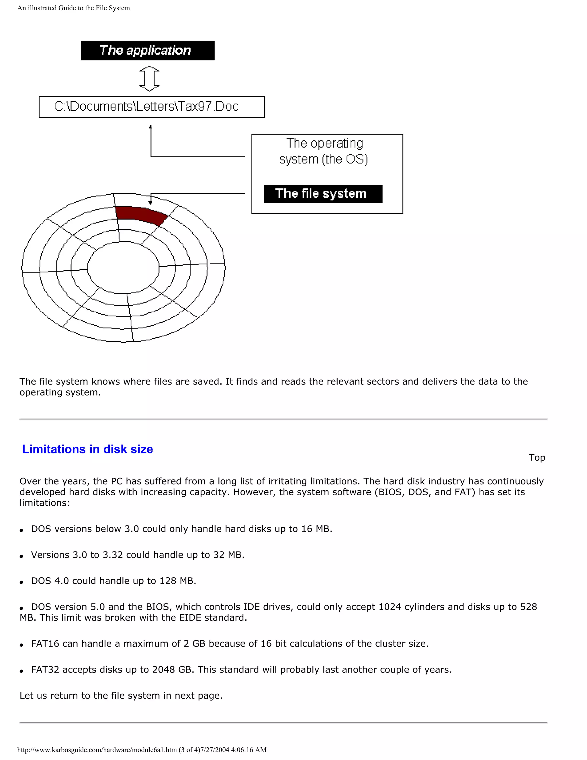
![An illustrated Guide to the File System
q Next page
q Previous page
Learn more Top
Read Windows tipswith a little about Windows 95/98.
Read Module 6c about the relationship between BIOS, OS and hardware
Read Module 7a about the videosystem
Read about video cards in Module 7b .
Read about digital sound in Module 7c .
[Main page] [Contact] [Karbo's Dictionary] [The Software Guides]
Copyright (c) 1996-2001 by Michael B. Karbo. www.karbosguide.com.
http://www.karbosguide.com/hardware/module6a1.htm (4 of 4)7/27/2004 4:06:16 AM](https://image.slidesharecdn.com/computerhardware-michaelkarbo-121118154249-phpapp01/75/Computer-hardware-michael-karbo-99-2048.jpg)
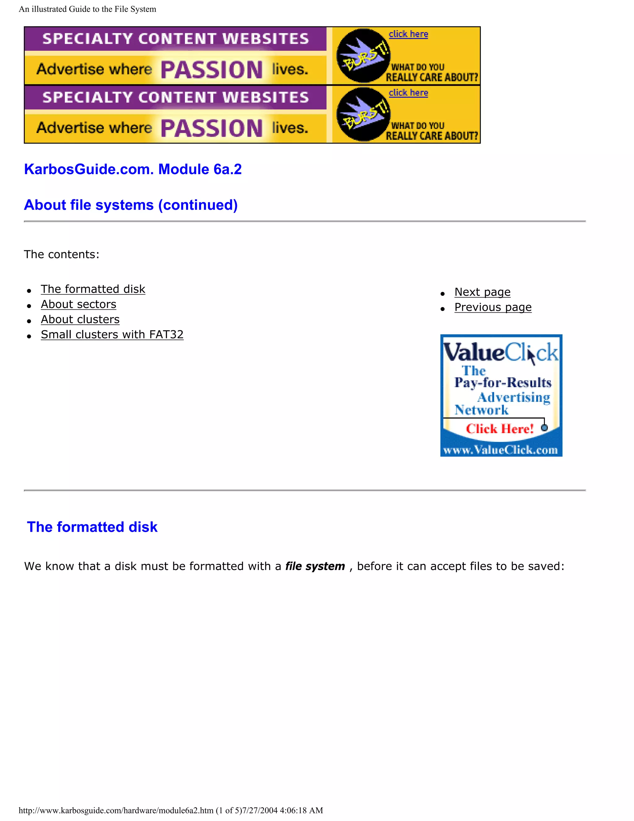
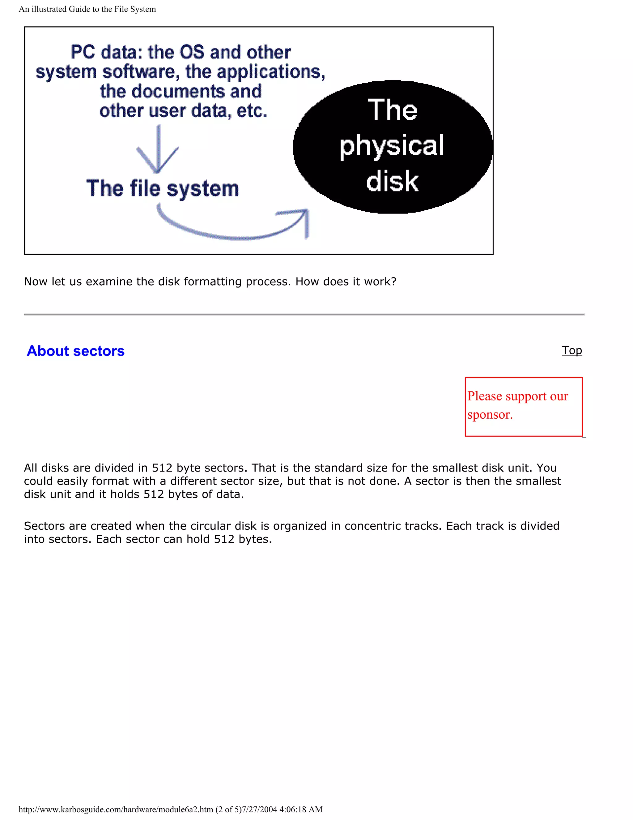
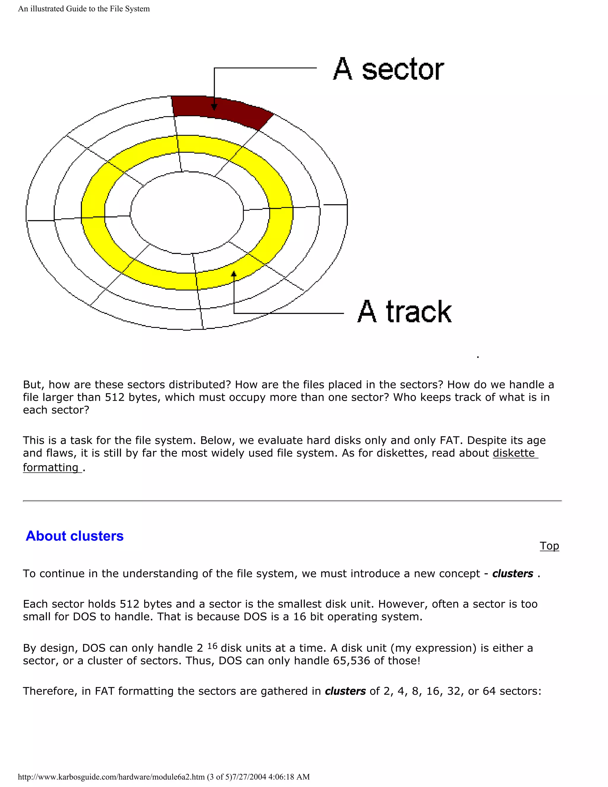
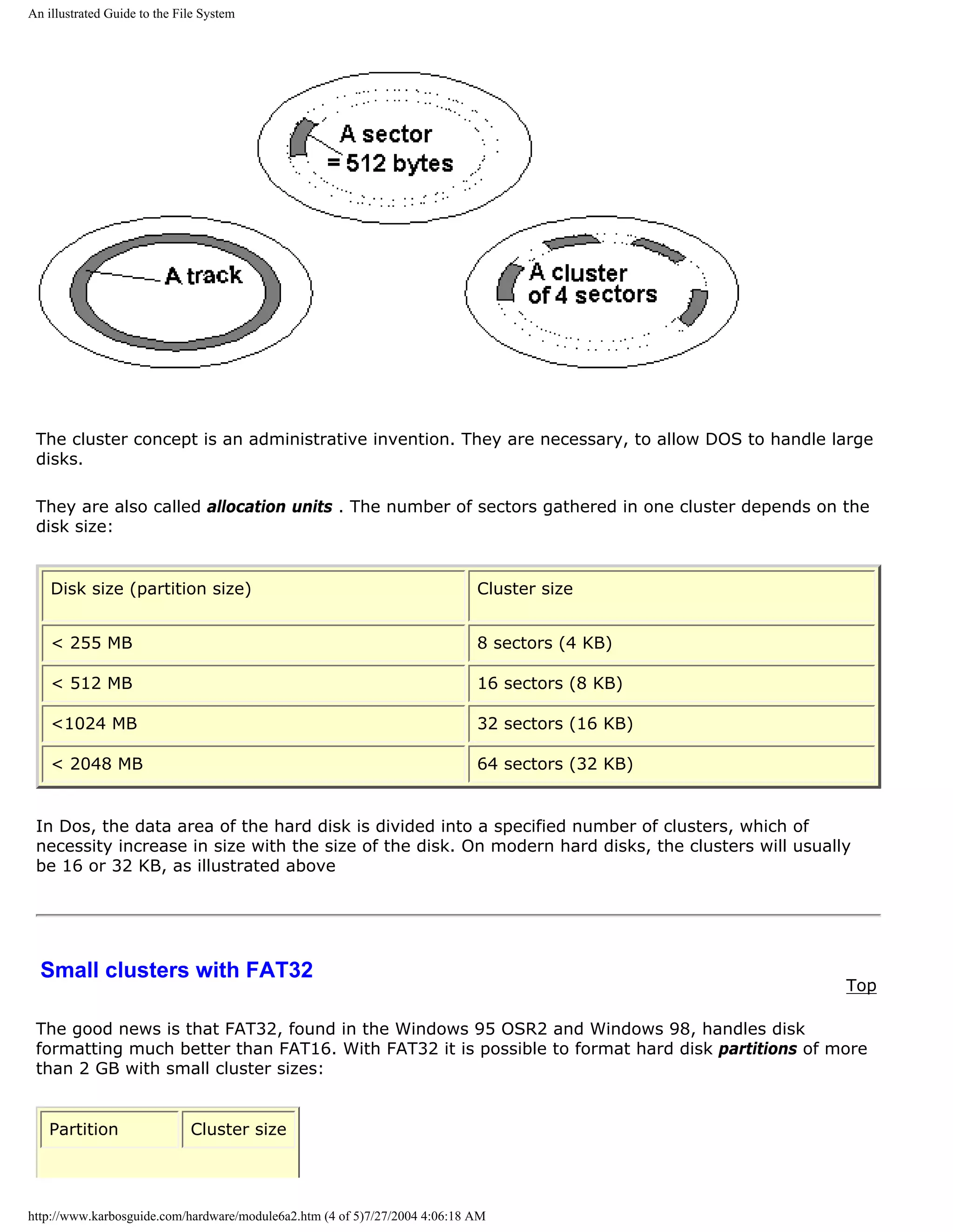
![An illustrated Guide to the File System
<8 GB 4 KB
8 GB - 16 GB 8 KB
16 GB - 32 GB 16 KB
> 32 GB 32 KB
Something else new in FAT32 is the moveable root directory, which can be of variable size. It
involves active use of both FATs (I cannot explain how). Altogether, it should make it simpler and
safer to change partition sizes. But the number of clusters per partition grows enormously in large
partitions.
FAT32 can only be installed in a new PC, since the partition has to be formatted in a special manner.
The file system is only available in the Windows 95 OSR2 (OEM Service Release 2) and in Windows
98.
q Next page
q Previous page
To learn more
Top
Read Module 6b with a little about Windows 95/98.
Read Module 6c about the relationship between BIOS, OS and hardware
Read Module 7a about the videosystem
Read about video cards in Module 7b .
Read about digital sound in Module 7c .
[Main page] [Contact] [Karbo's Dictionary] [The Software Guides]
http://www.karbosguide.com/hardware/module6a2.htm (5 of 5)7/27/2004 4:06:18 AM](https://image.slidesharecdn.com/computerhardware-michaelkarbo-121118154249-phpapp01/75/Computer-hardware-michael-karbo-104-2048.jpg)
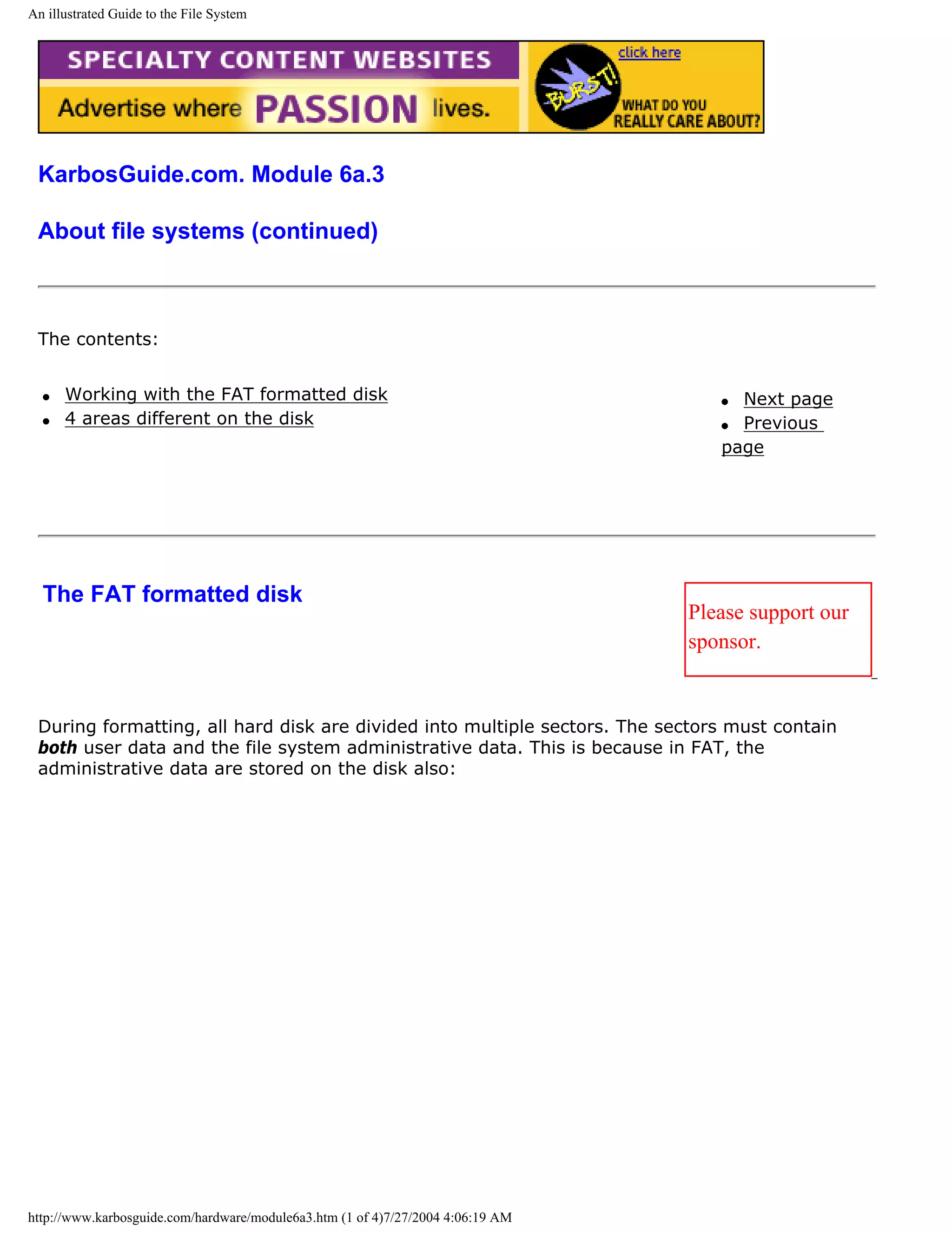
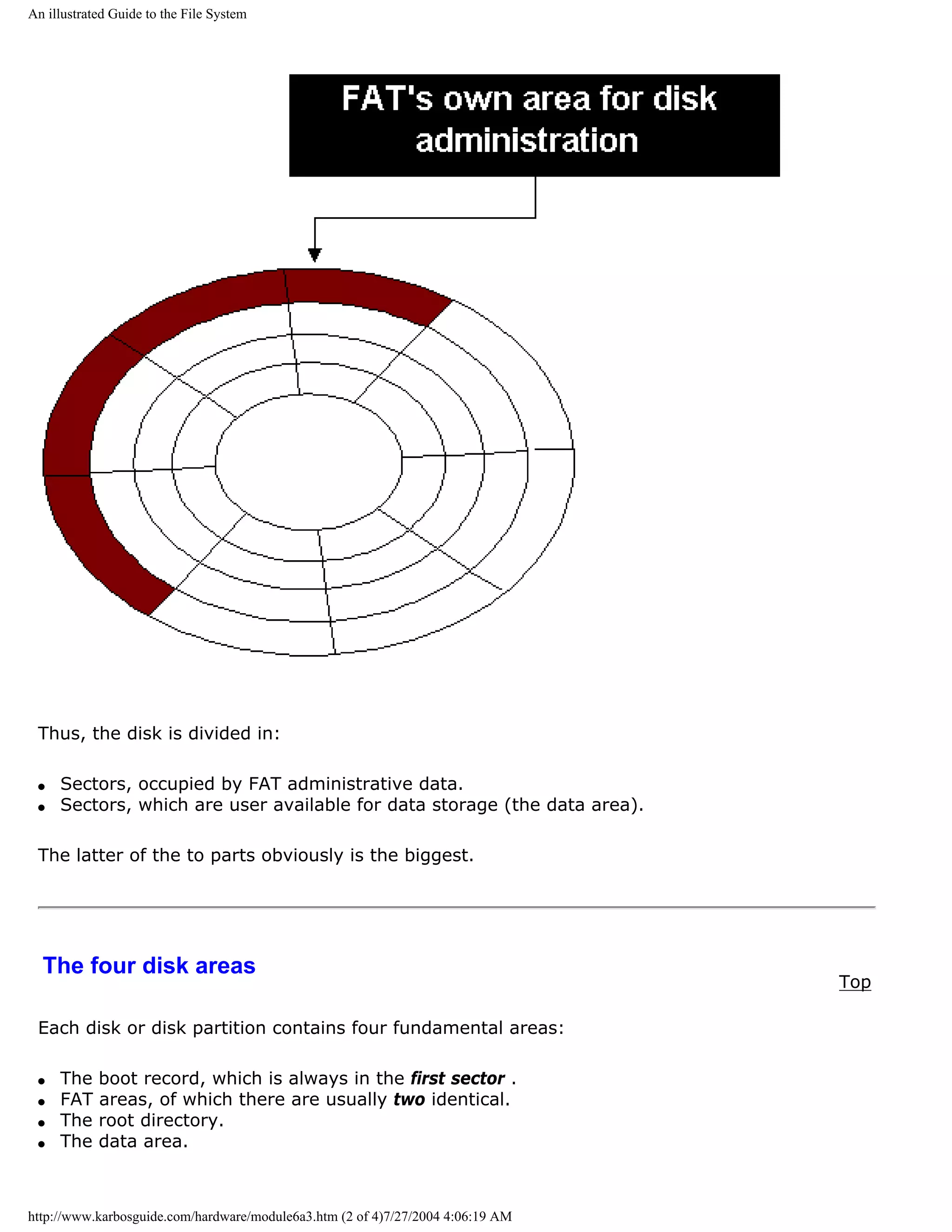
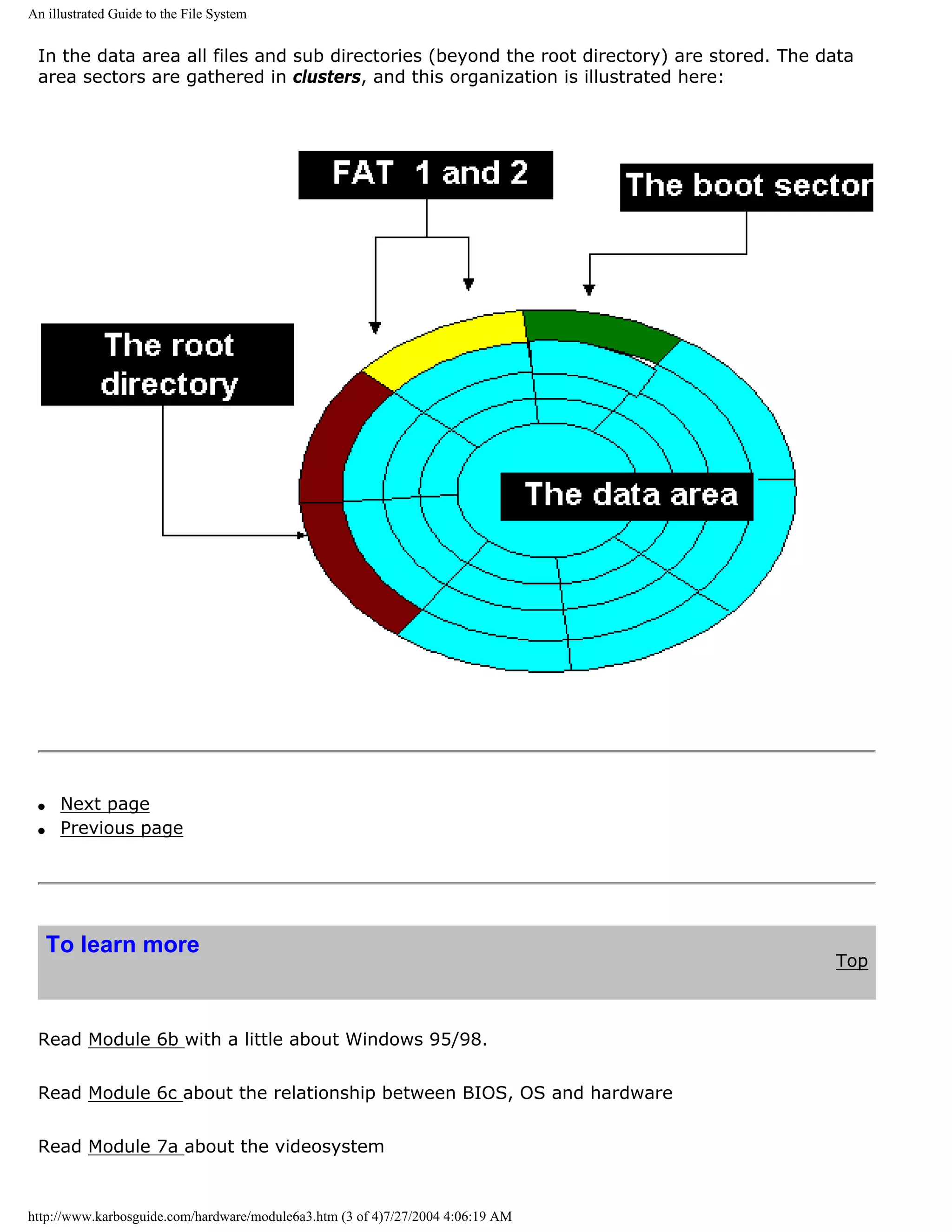
![An illustrated Guide to the File System
Read about video cards in Module 7b .
Read about digital sound in Module 7c .
[Main page] [Contact] [Karbo's Dictionary] [The Software Guides]
Copyright (c) 1996-2001 by Michael B. Karbo. www.karbosguide.com.
http://www.karbosguide.com/hardware/module6a3.htm (4 of 4)7/27/2004 4:06:19 AM](https://image.slidesharecdn.com/computerhardware-michaelkarbo-121118154249-phpapp01/75/Computer-hardware-michael-karbo-108-2048.jpg)
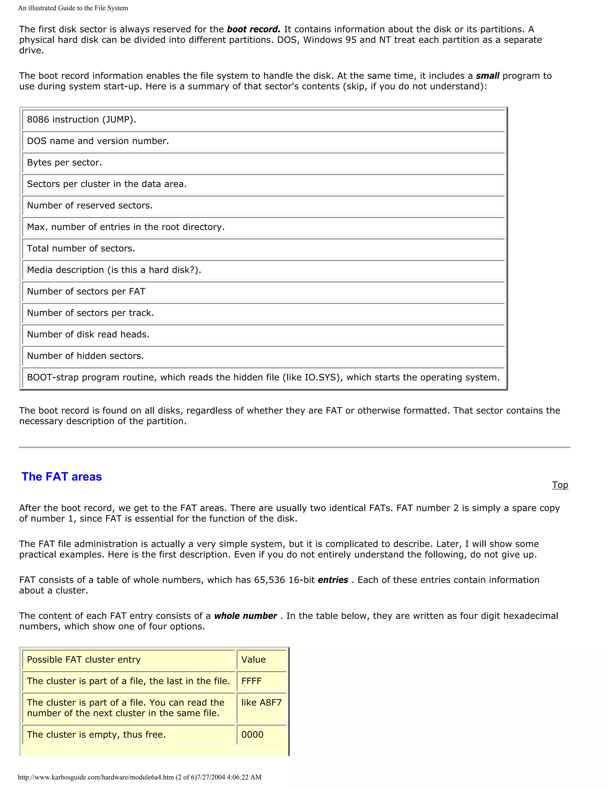
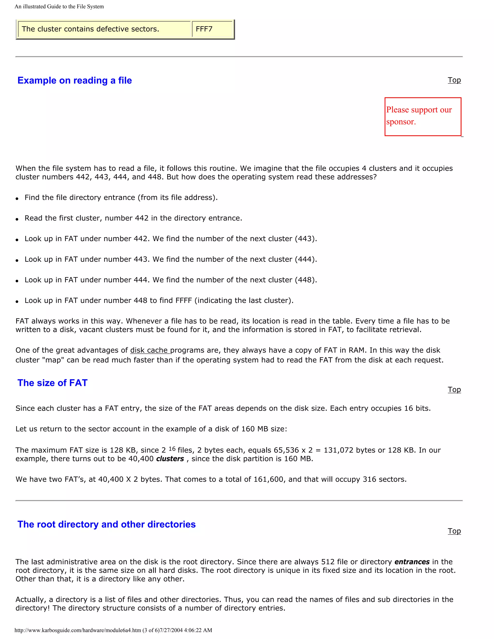
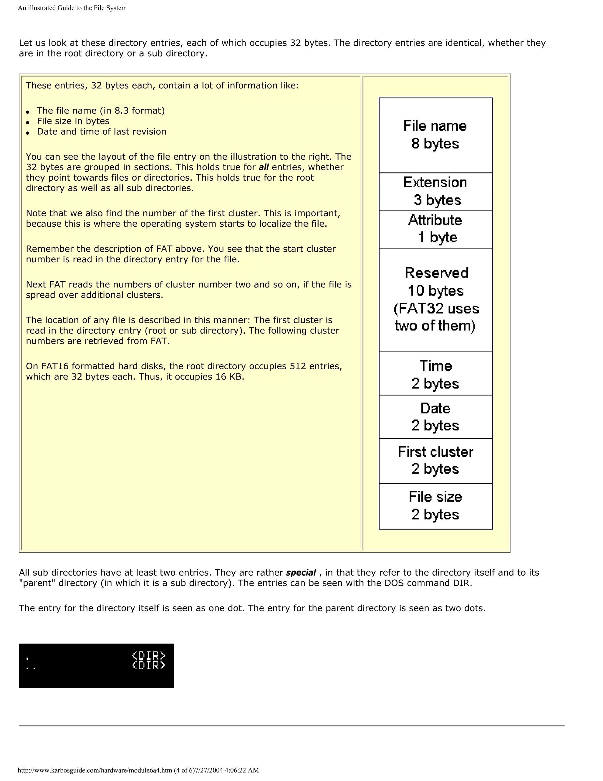
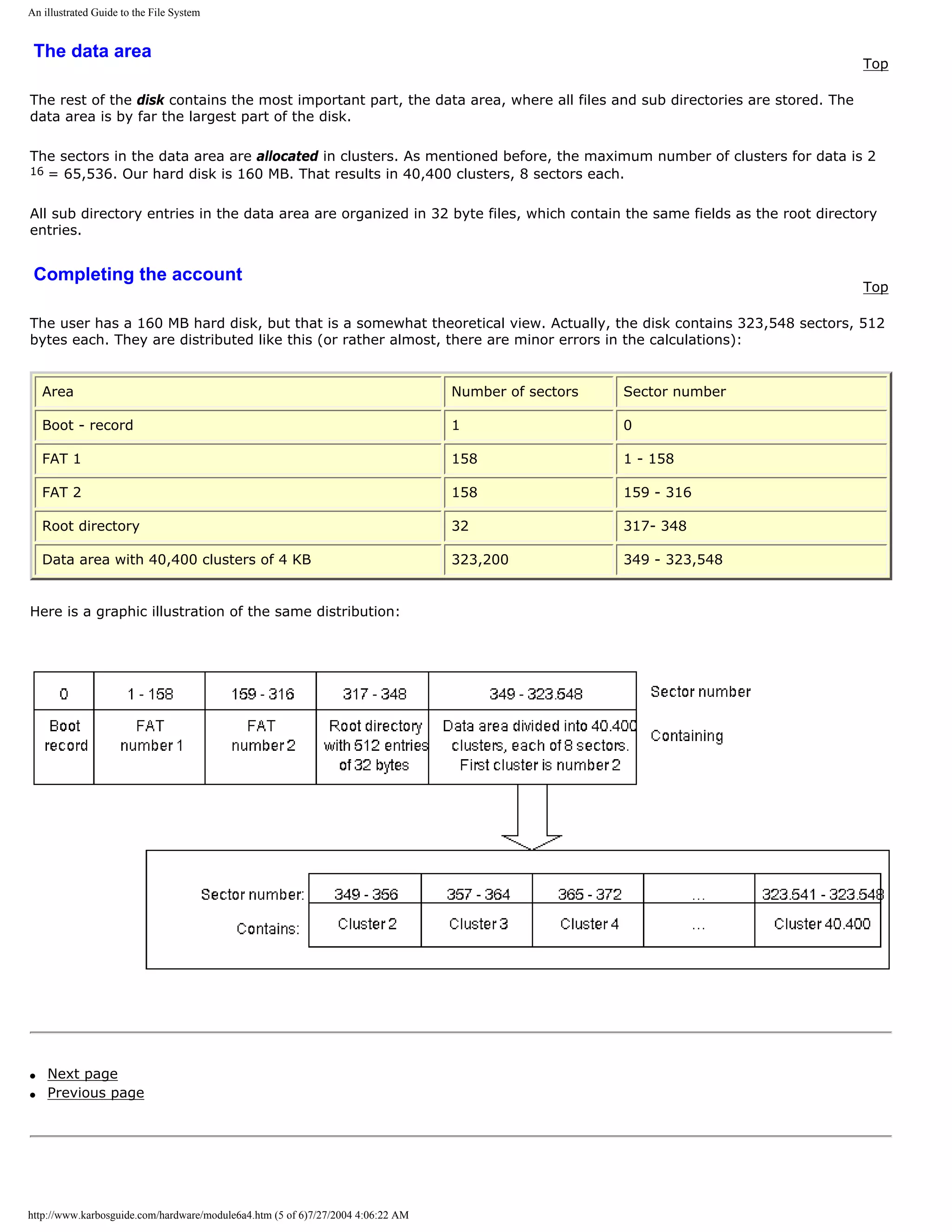
![An illustrated Guide to the File System
To learn more
Top
Read Module 6b with a little about Windows 95/98.
Read Module 6c about the relationship between BIOS, OS and hardware
Read Module 7a about the videosystem
Read about video cards in Module 7b .
Read about digital sound in Module 7c .
[Main page] [Contact] [Karbo's Dictionary] [The Software Guides]
Copyright (c) 1996-2001 by Michael B. Karbo. www.karbosguide.com.
http://www.karbosguide.com/hardware/module6a4.htm (6 of 6)7/27/2004 4:06:22 AM](https://image.slidesharecdn.com/computerhardware-michaelkarbo-121118154249-phpapp01/75/Computer-hardware-michael-karbo-114-2048.jpg)
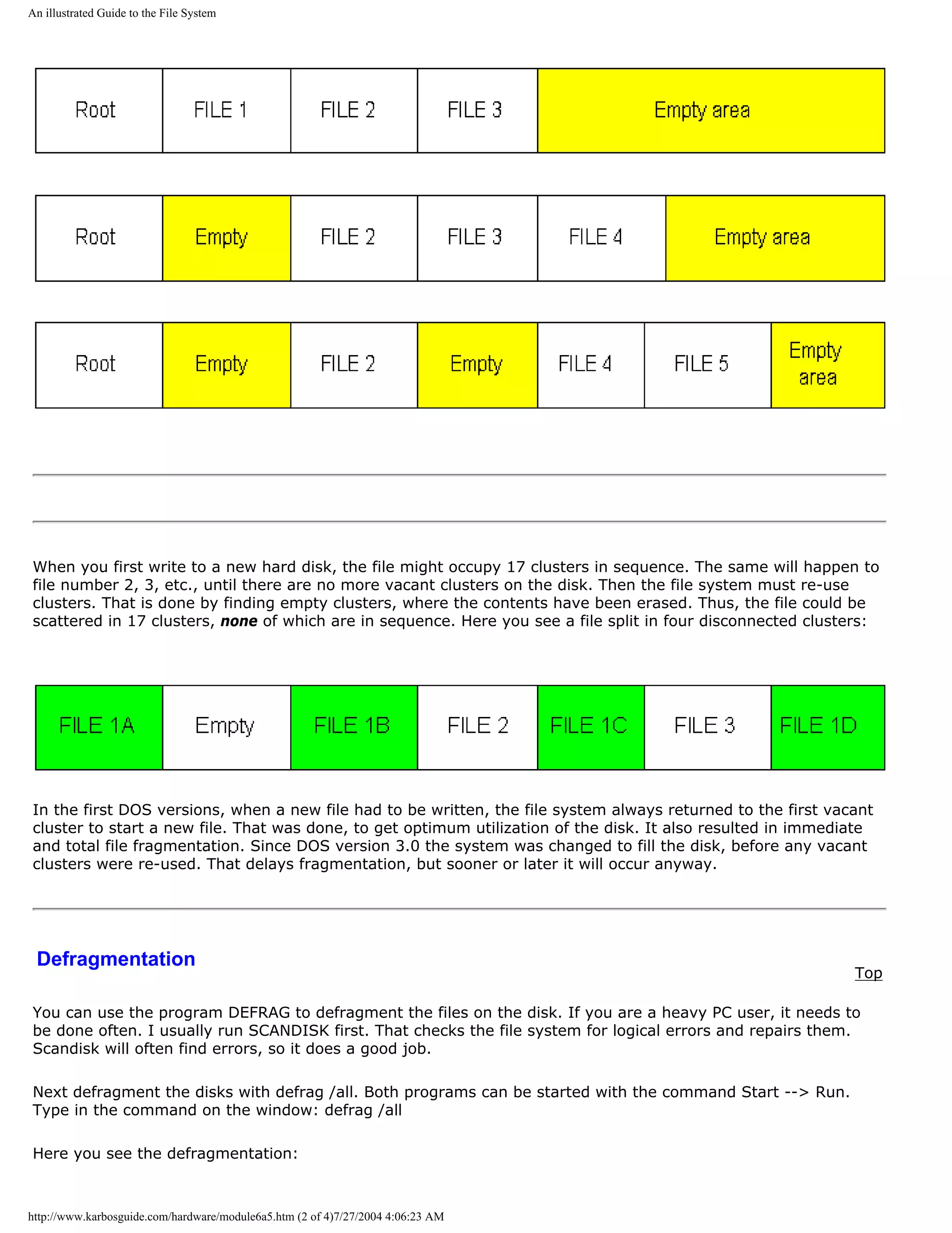
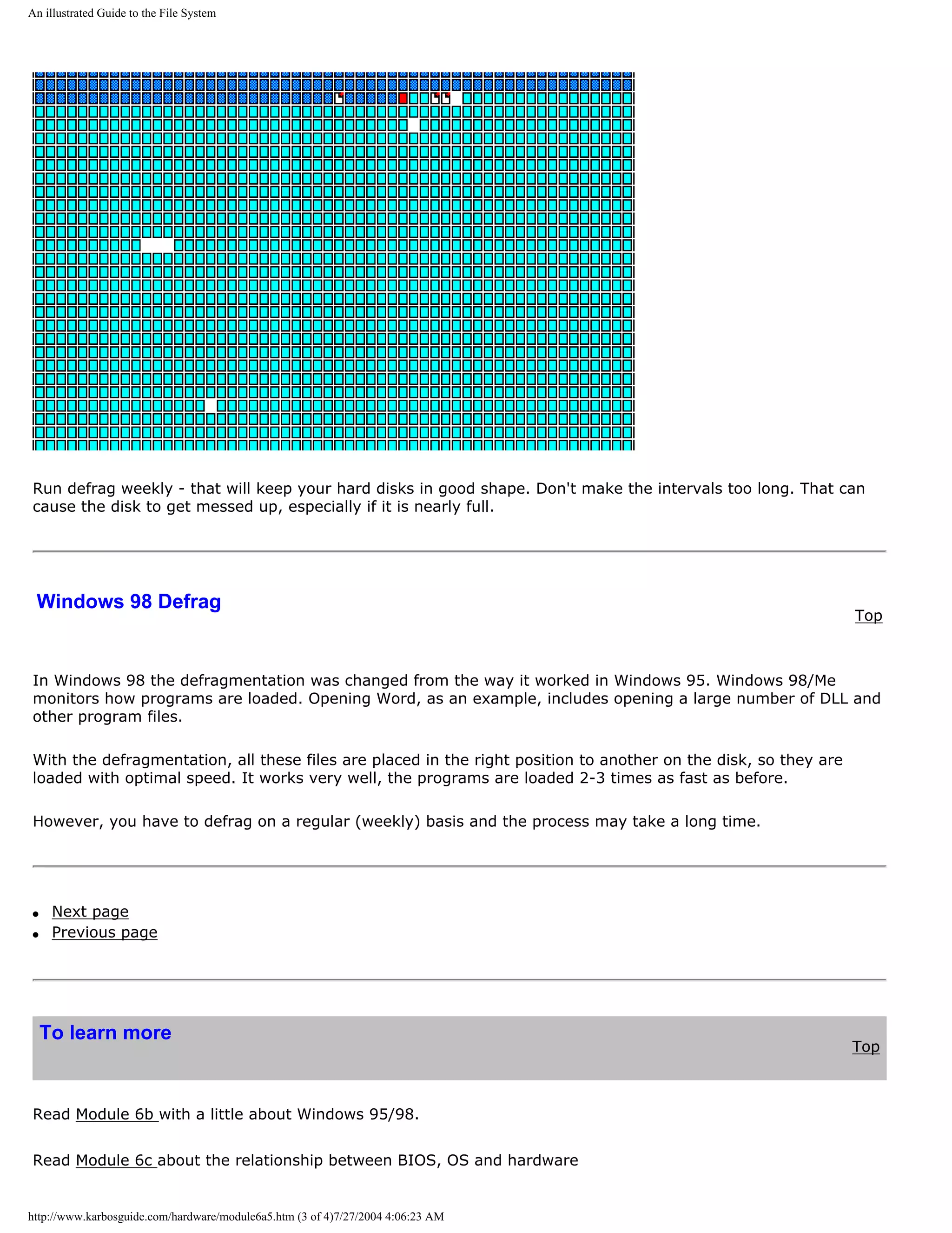
![An illustrated Guide to the File System
Read Module 7a about the videosystem
Read about video cards in Module 7b .
Read about digital sound in Module 7c .
[Main page] [Contact] [Karbo's Dictionary] [The Software Guides]
Copyright (c) 1996-2001 by Michael B. Karbo. www.karbosguide.com.
http://www.karbosguide.com/hardware/module6a5.htm (4 of 4)7/27/2004 4:06:23 AM](https://image.slidesharecdn.com/computerhardware-michaelkarbo-121118154249-phpapp01/75/Computer-hardware-michael-karbo-118-2048.jpg)
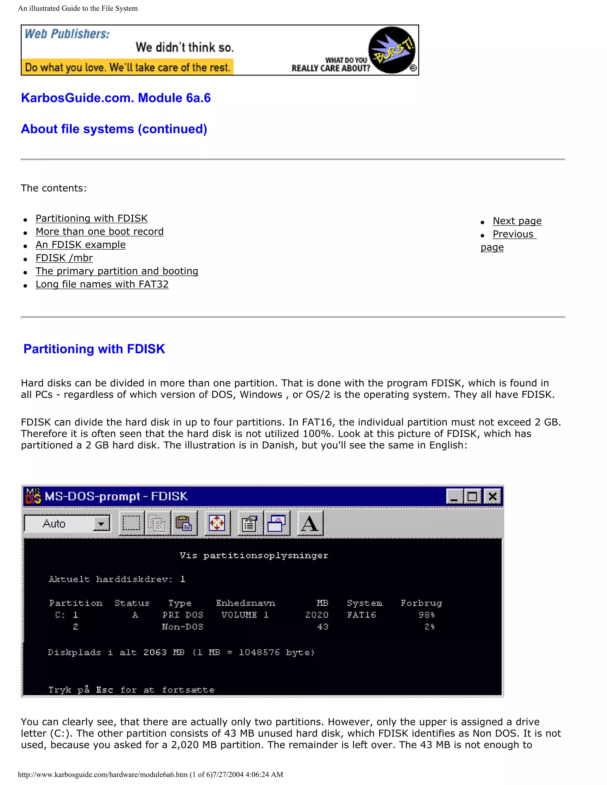
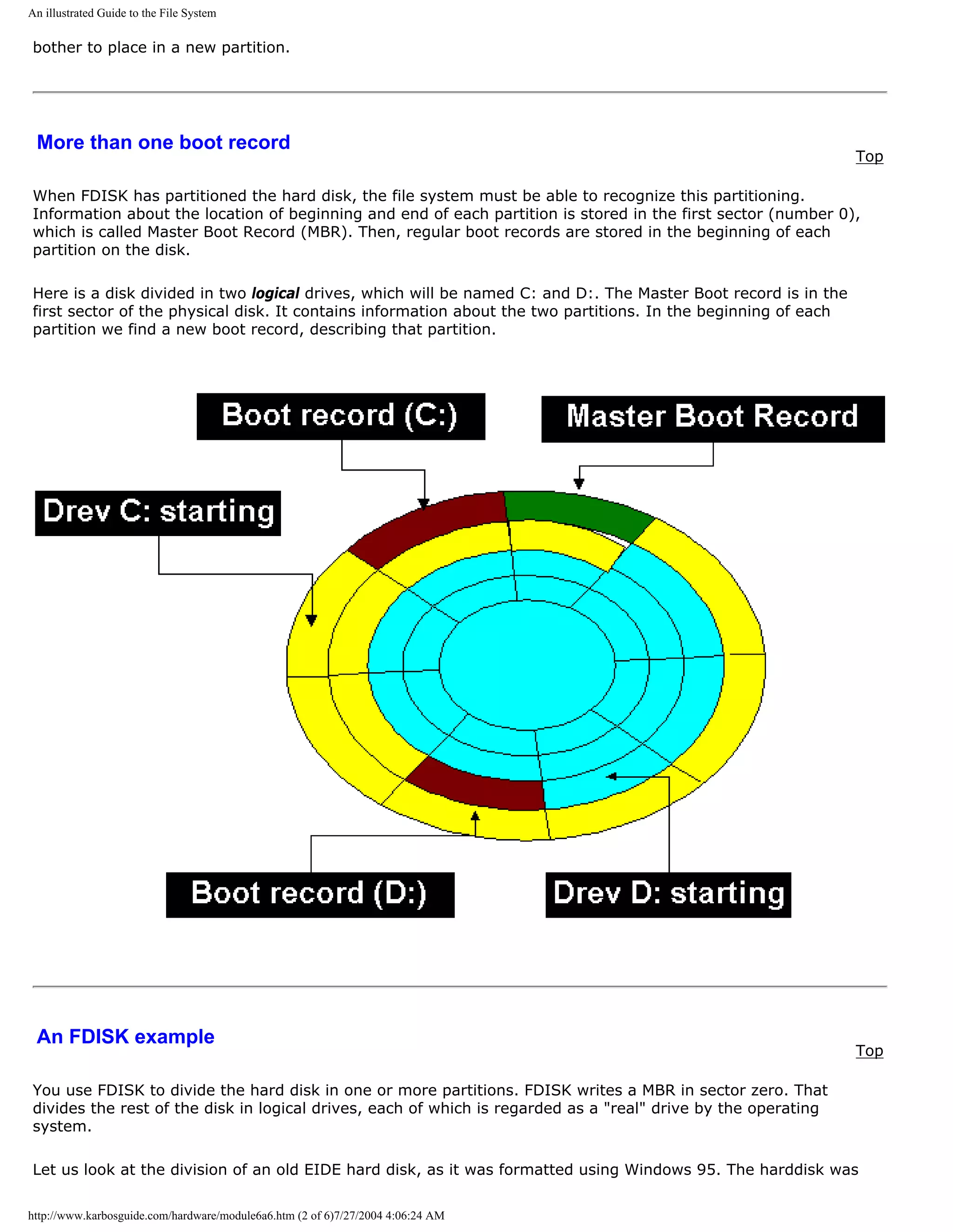
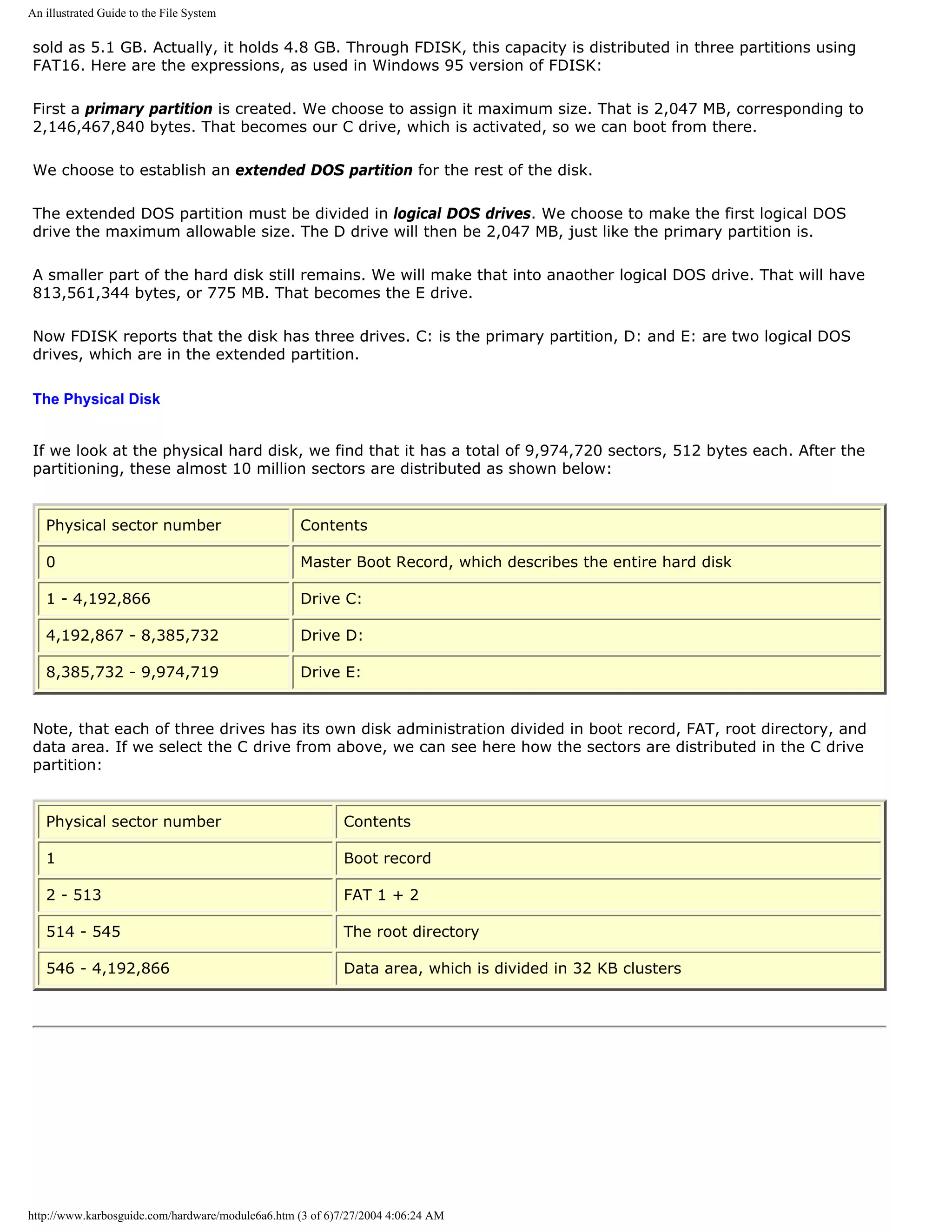
![An illustrated Guide to the File System
directories, each of which provides 32 bytes to the file name.
You should be happy about the long file names in Windows - it makes it much easier to identify saved files. The
only "danger" is, that you must not defragment the hard disk with a DOS based application. Then the long file
names are destroyed. The files still exist, but you can only find them under their 8.3 name and that is an
annoying experience, especially if you have thousands of files.
However, you should not waste memory and disk space using filenames 50 characters long. Usually filenames
of 15-20 characters work fine.
q Next page
q Previous page
To learn more
Top
Read Module 6b with a little about Windows 95/98.
Read Module 7a about the videosystem
Read about video cards in Module 7b .
Read about digital sound in Module 7c .
[Main page] [Contact] [Karbo's Dictionary] [The Software Guides]
Copyright (c) 1996-2001 by Michael B. Karbo. www.karbosguide.com.
http://www.karbosguide.com/hardware/module6a6.htm (6 of 6)7/27/2004 4:06:24 AM](https://image.slidesharecdn.com/computerhardware-michaelkarbo-121118154249-phpapp01/75/Computer-hardware-michael-karbo-124-2048.jpg)
![An illustrated guide to Operating Systems and the use ofhardware drivers
KarbosGuide.com. Module 6c1.
About operating systems and driver programs
The contents:
q What is an operating system? q Next page
q The operating system recognizes hardware q Previous page
On the following pages:
q BIOS or driver programs
q Which operating systems?
q DOS control of hardware
q 32 bit drivers and installation
Click & Learn deals primarily with hardware. In these pages I will cover the operating system
as it connects downward towards hardware. The operating system is closely associated with
the ROM BIOS program routines, which are described in module 2a . The two program layers
(operating system + BIOS) are called system software and it is very useful to understand
their importance for the PC.
Let us start by studying what an operating system really is.
What is an operating system? [top]
Please support our
sponsor.
Traditionally the operating system consists of three parts:
http://www.karbosguide.com/hardware/module6c1.htm (1 of 5)7/27/2004 4:06:26 AM](https://image.slidesharecdn.com/computerhardware-michaelkarbo-121118154249-phpapp01/75/Computer-hardware-michael-karbo-126-2048.jpg)
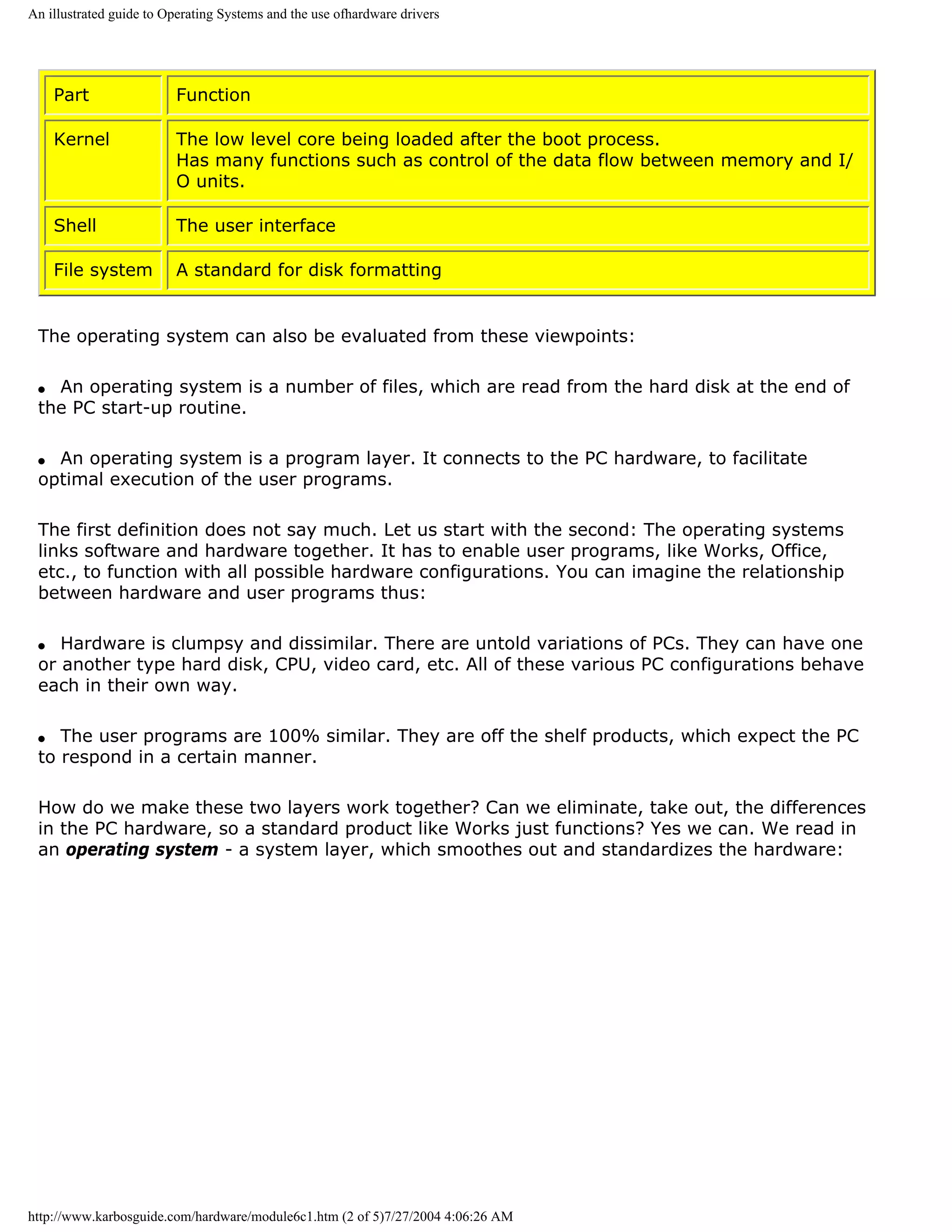
![An illustrated guide to Operating Systems and the use ofhardware drivers
You should understand the operating system as a necessary layer, which smoothes out
bumps and pot holes in your PC's hardware. This will give the user programs a stable, even
work platform.
The operating system recognizes hardware
[top]
The PC's hardware represents resources relative to the user program.
Think of your word processing program: You want to print your text. The program issues a
print order, expecting that the document will be printed as designed. The word processing
program dispatches data according to your commands. How they are translated to signals
understood by your printer - that is not the word processing program's problem. The printer
is a resource relative to the word processing program. The connections to these resources is
via the operating system. This holds true for all the resources, which are included in the PC
hardware:
http://www.karbosguide.com/hardware/module6c1.htm (3 of 5)7/27/2004 4:06:26 AM](https://image.slidesharecdn.com/computerhardware-michaelkarbo-121118154249-phpapp01/75/Computer-hardware-michael-karbo-128-2048.jpg)
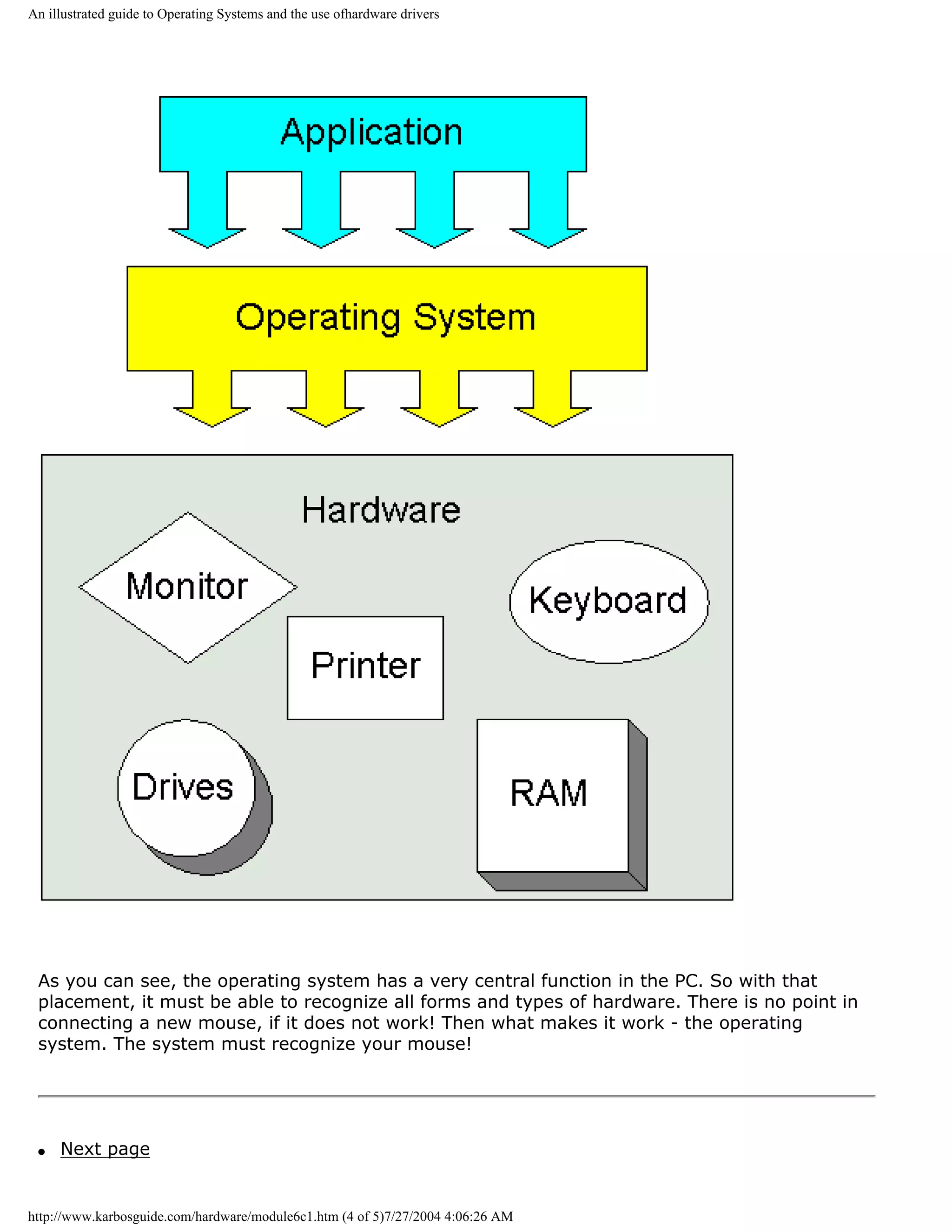
![An illustrated guide to Operating Systems and the use ofhardware drivers
q Previous page
Learn more [top]
Also see The Software Tips
Read of module 7a and module 7b about installation monitor and video card in Windows
95/98!
Read about chip sets on the motherboard in module 2d
Read module 5a about expansion cards, where we evaluate the I/O buses from the port side.
[Main page] [Contact] [Karbo's Dictionary] [The Software Guides]
Copyright (c) 1996-2001 by Michael B. Karbo. www.karbosguide.com.
http://www.karbosguide.com/hardware/module6c1.htm (5 of 5)7/27/2004 4:06:26 AM](https://image.slidesharecdn.com/computerhardware-michaelkarbo-121118154249-phpapp01/75/Computer-hardware-michael-karbo-130-2048.jpg)
![An illustrated guide to Operating Systems and the use ofhardware drivers
KarbosGuide.com. Module 6c2.
About OSs and drivers - continued
The contents:
q System software q Next page
q BIOS or driver programs q Previous page
System software
[top]
Together, the operating system and the ROM BIOS program routines form the layer on which
the user programs "rest." When the PC has to work, an operating system has to be read from
a disk. There are many different operating systems to choose from. However, the BIOS is
always placed firmly and centrally in the PC hardware.
Please support our
BIOS - firmware
sponsor.
One of the fundamental techniques in the PC design is the BIOS program layer. BIOS (Basic
Input Output System) is a group of small programs, furnished by the PC manufacturer - also
called firmware .
http://www.karbosguide.com/hardware/module6c2.htm (1 of 5)7/27/2004 4:06:28 AM](https://image.slidesharecdn.com/computerhardware-michaelkarbo-121118154249-phpapp01/75/Computer-hardware-michael-karbo-131-2048.jpg)
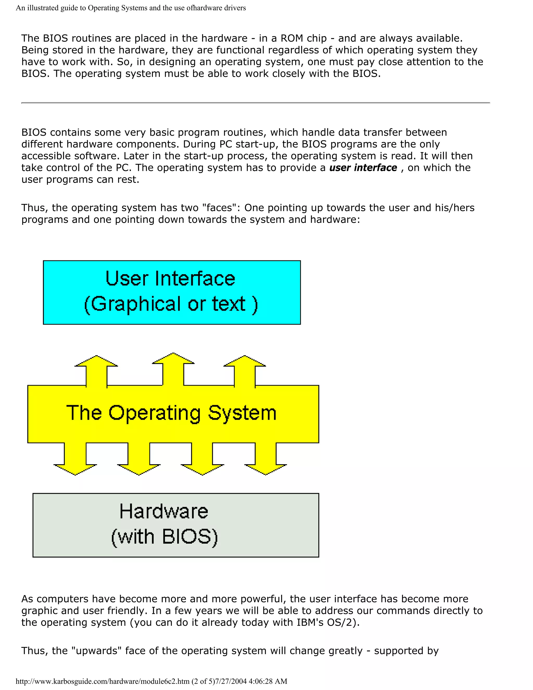
![An illustrated guide to Operating Systems and the use ofhardware drivers
technological development. The "downwards" face - the operating system's interface with
hardware - will change less. At least, the fundamental principles are the same as in the
childhood of the PC.
BIOS or drive programs
[top]
The operating system must be able to communicate with hardware. As we are going to see,
this can be done in two ways:
q The operating system communicates directly with hardware through drive programs.
q The operating system utilizes the BIOS programs.
While BIOS is hardware specific program code, stored in hardware, the drive programs are
small hardware specific program elements read from the disk together with the operating
system.
Depending on which operating system is installed, both principles are used in various
degrees. Since the BIOS programs consist of 16 bit code, it is typically DOS (a 16 bit
operating system) which utilizes BIOS to a large degree. In the newer 32 bit operating
systems, it is not efficient to use BIOS any more than necessary.
Here is a model, which shows the operating system with BIOS and drive programs (usually
just called drivers ):
http://www.karbosguide.com/hardware/module6c2.htm (3 of 5)7/27/2004 4:06:28 AM](https://image.slidesharecdn.com/computerhardware-michaelkarbo-121118154249-phpapp01/75/Computer-hardware-michael-karbo-133-2048.jpg)
![An illustrated guide to Operating Systems and the use ofhardware drivers
As you can see, the driver/BIOS functions are closely associated with the operating system.
So let us look at that on the following page.
q Next page
q Previous page
Learn more [top]
Also see The Software Tips
Read of module 7a and module 7b about installation monitor and video card in Windows
95/98!
http://www.karbosguide.com/hardware/module6c2.htm (4 of 5)7/27/2004 4:06:28 AM](https://image.slidesharecdn.com/computerhardware-michaelkarbo-121118154249-phpapp01/75/Computer-hardware-michael-karbo-134-2048.jpg)
![An illustrated guide to Operating Systems and the use ofhardware drivers
Read about chip sets on the motherboard in module 2d
Read module 5a about expansion cards, where we evaluate the I/O buses from the port side.
[Main page] [Contact] [Karbo's Dictionary] [The Software Guides]
Copyright (c) 1996-2001 by Michael B. Karbo. www.karbosguide.com.
http://www.karbosguide.com/hardware/module6c2.htm (5 of 5)7/27/2004 4:06:28 AM](https://image.slidesharecdn.com/computerhardware-michaelkarbo-121118154249-phpapp01/75/Computer-hardware-michael-karbo-135-2048.jpg)
![An illustrated guide to Operating Systems and the use ofhardware drivers
KarbosGuide.com. Module 6c3.
About OSs and drivers - continued
The contents:
q Which operating systems? q Next page
q DOS control of hardware q Previous page
Which operating systems?
[top]
The operating systems have undergone a tremendous development since 1981. It all started with DOS, which
was a 16 bit modification of a simple 8 bit operating system called CP/M.
DOS was further developed in the 1980s. Since around 1990 Windows came into the scene. Windows started as a
GUI ( Graphic User Interface ) for DOS.
The PC booted with DOS as operating system. Then you could choose, if you wanted mouse and graphics on the
screen with Windows . Windows was a supplement to DOS.
The Graphic User Interface (GUI) allows you to work with a mouse instead of writing long command lines like
copy c:texts*.* d:textbak *.* /s/v/, which is the standard in text based operating systems (like DOS).
DOS was designed for 16 bit computers, which the first PCs were. With Intel's 80386 the 32 bit technology was
knocking at the door. Modern PCs are designed for straight 32 bit program execution. So we have seen a gradual
trend in the PC operating systems from 16 bit towards 32 bit and this affects hardware design.
http://www.karbosguide.com/hardware/module6c3.htm (1 of 5)7/27/2004 4:06:30 AM](https://image.slidesharecdn.com/computerhardware-michaelkarbo-121118154249-phpapp01/75/Computer-hardware-michael-karbo-136-2048.jpg)
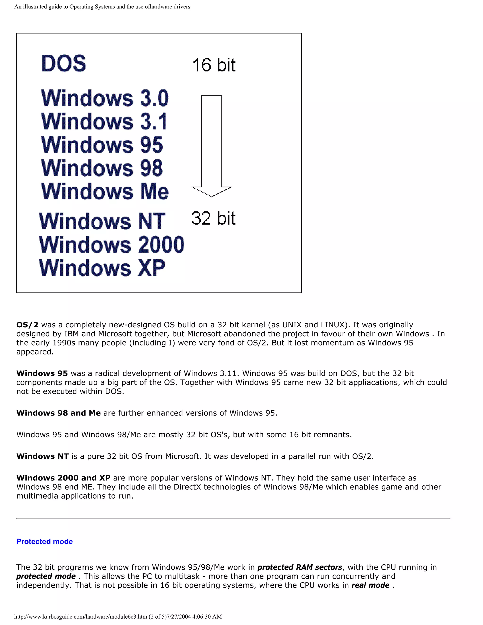
![An illustrated guide to Operating Systems and the use ofhardware drivers
A brief comparison of 16 bit and 32 bit operating systems can look like this:
Operating system DOS 32 bit operating system (NT, OS/2, UNIX)
Users Single user Multiple users
Program execution 16 bit single task in real mode 32 bit multitask in protected mode
Screen appearance Mostly Text based (poor quality Often GUI - graphic interface with high
graphics) resolution graphics
Hardware handling Primarily BIOS Custom designed 32 bit drivers for each
hardware component.
DOS control of hardware [top]
Please support our
sponsor.
DOS is quite simple to describe, since it principally consists of only 4 parts:
q A boot record, which activates the operating system.
q The file IO.SYS, which is interfaced to ROM BIOS with installation of device drivers .
q The file MSDOS.SYS. That is the core of DOS, handling the file system and program execution.
q The file COMMAND.COM, which provides the command line, the text based user interface.
When we talk about hardware control, it is done through IO.SYS. That is a program which reads the ROM BIOS
code and converts it to DOS's own device drivers.
The smart thing about DOS is that the operating system can be expanded with external device drivers. IO.SYS
reads them via the start-up file CONFIG.SYS. First device drivers are read from ROM BIOS. Then any possible
additional drivers are read from disk. In that way DOS can handle hardware units which did not exist when the
PC was originally configured.
A final option to handle hardware from DOS programs is to write special drivers for the individual user program .
Many DOS games come with their own graphics drivers (they have to recognize all graphics standards on the
market!). Another classic example is the word processing program WordPerfect, which in its prime (version 5.1)
came with drivers to more than 500 different printers!
Unit Example of DOS device drivers
Hard disk BIOS
Video card BIOS
Mouse MOUSE.SYS
http://www.karbosguide.com/hardware/module6c3.htm (3 of 5)7/27/2004 4:06:30 AM](https://image.slidesharecdn.com/computerhardware-michaelkarbo-121118154249-phpapp01/75/Computer-hardware-michael-karbo-138-2048.jpg)
![An illustrated guide to Operating Systems and the use ofhardware drivers
CD-ROM ATAPI.SYS + MSCDEX.EXE
Printer Internal drivers in the user program (like WordPerfect 5.1)
The device drivers can be seen with the program MSD. Here is a picture from Windows 95, where you can clearly
see the names of the device drivers (CON, PRN, LPT1 etc.):
All these device drivers are in 16 bit program code.
q Next page
q Previous page
Learn more [top]
Also see The Software Tips
Read of module 7a and module 7b about installation monitor and video card in Windows 95/98!
http://www.karbosguide.com/hardware/module6c3.htm (4 of 5)7/27/2004 4:06:30 AM](https://image.slidesharecdn.com/computerhardware-michaelkarbo-121118154249-phpapp01/75/Computer-hardware-michael-karbo-139-2048.jpg)
![An illustrated guide to Operating Systems and the use ofhardware drivers
Read about chip sets on the motherboard in module 2d
Read module 5a about expansion cards, where we evaluate the I/O buses from the port side.
[Main page] [Contact] [Karbo's Dictionary] [The Software Guides]
Copyright (c) 1996-2001 by Michael B. Karbo. www.karbosguide.com.
http://www.karbosguide.com/hardware/module6c3.htm (5 of 5)7/27/2004 4:06:30 AM](https://image.slidesharecdn.com/computerhardware-michaelkarbo-121118154249-phpapp01/75/Computer-hardware-michael-karbo-140-2048.jpg)
![An illustrated guide to Operating Systems and the use ofhardware drivers
Please click the banners to support our work!
KarbosGuide.com. Module 6c4.
About OSs and drivers - continued
The contents:
q 32 bit drivers q Next page
q Installation of new drivers q Previous page
32 bit drivers
[top]
In 32 bit operating systems, you use 32 bit drivers instead of ROM BIOS. This means that software suppliers like Microsoft and IBM must be able to supply drivers
to all conceivable hardware. The advantage is, that once the operating system has installed drivers, all user programs operate alike relative to hardware.
It is an enormous project to supply drivers. Especially OS/2 has suffered problems in getting the right drivers on the market. For many years, IBM for example did
not supply OS/2 drivers for Canon printers. That was part of my reason to drop that operating system. Regarding driver installations, Windows 98 is
unquestionably the best operating system.
Windows supports plug and play. The operating system searches the PC for hardware. Often all drivers (to CD-ROM, network controller, sound card, etc.) are
installed automatically. The drivers can be seen under System in the control panel.
Let us look at a EIDE hard disk. The hard disk operation is regulated by an EIDE controller on the system board. Therefore, Windows must have a driver installed
to this controller. We can find it easily. Go to: My computer -> Control panel -> System -> Computer. In Windows 2000 you should click on Device manager:
http://www.karbosguide.com/hardware/module6c4.htm (1 of 6)7/27/2004 4:06:33 AM](https://image.slidesharecdn.com/computerhardware-michaelkarbo-121118154249-phpapp01/75/Computer-hardware-michael-karbo-141-2048.jpg)
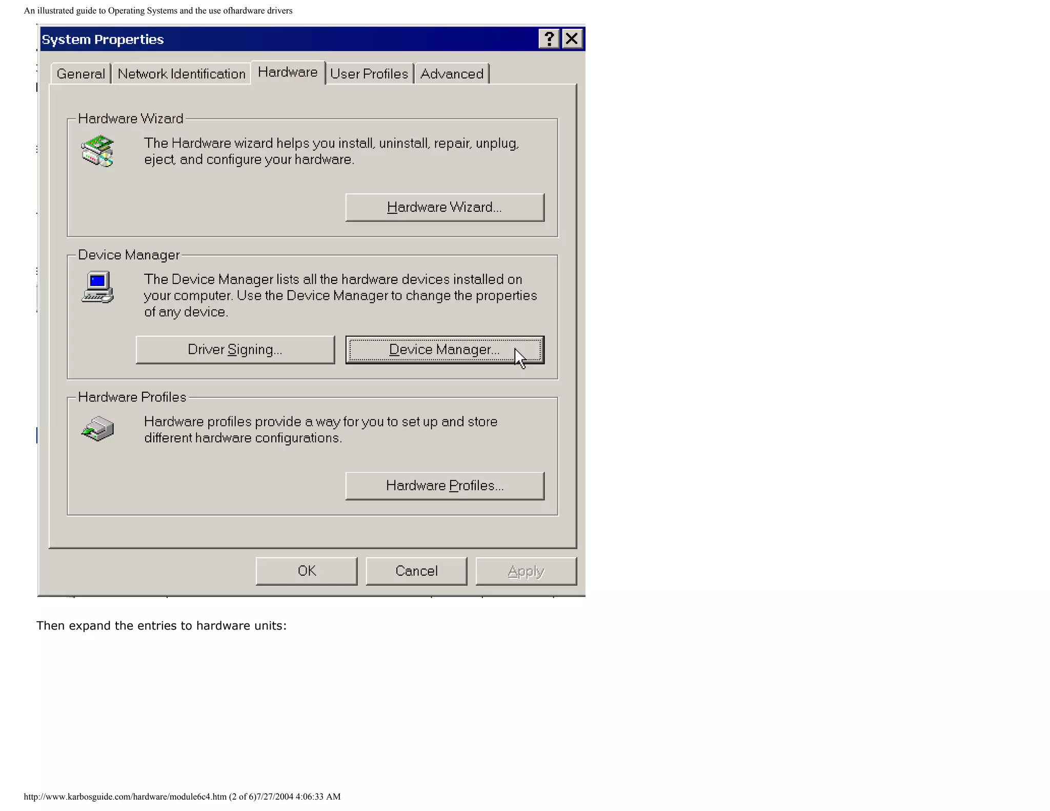
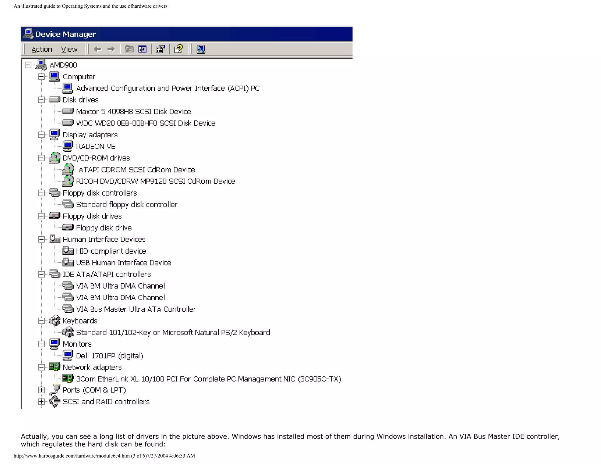
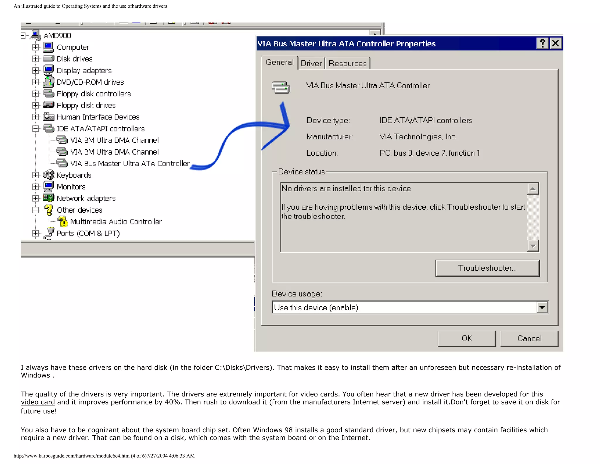
![An illustrated guide to Operating Systems and the use ofhardware drivers
Installation of new drivers [top]
Please support our
sponsor.
You install new drivers in Windows 98/Me/2000 with "add new hardware" found in My Computer -> Control panel:.
http://www.karbosguide.com/hardware/module6c4.htm (5 of 6)7/27/2004 4:06:33 AM](https://image.slidesharecdn.com/computerhardware-michaelkarbo-121118154249-phpapp01/75/Computer-hardware-michael-karbo-145-2048.jpg)
![An illustrated guide to Operating Systems and the use ofhardware drivers
Don't let Windows search for hardware. Instead choose yourself. Then you have to select the particular hardware from the list and in the next screen click "Have
diskette... " Learn this technique if you experiment with your PC and want maximal benefits from your hardware.
q Next page
q Previous page
Learn more [top]
Also see The Windows 98 page (module 6d)
Read of module 7a and module 7b about installation monitor and video card in Windows 95/98!
Read about chip sets on the motherboard in module 2d
Read module 5a about expansion cards, where we evaluate the I/O buses from the port side.
[Main page] [Contact] [Karbo's Dictionary] [The Software Guides]
http://www.karbosguide.com/hardware/module6c4.htm (6 of 6)7/27/2004 4:06:33 AM](https://image.slidesharecdn.com/computerhardware-michaelkarbo-121118154249-phpapp01/75/Computer-hardware-michael-karbo-146-2048.jpg)
![An illustrated Guide to Monitors and the Video System
Please click the banners to support our work!
KarbosGuide.com. Module 7
q About the video system
q About video cards
q About sound cards
q About digital sound and music.
The contents on this and following pages:
q Introduction q Next page
q Concepts and terminology q Previous page
q Screen resolution, screen size etc.
q About colors, color depth, RGB etc.
q About refresh rates
q TCO standards
q LCD displays
The video system (of which the monitor is a part) is one of the most
important components in the PC. It affects directly your pleasure of working,
and actually also your health. At the same time, the video system shows the
biggest variation between different PCs. Read my coverage of this subject
here in this module, which is subdivided into several pages.
Introduction
[top]
All computers are connected to some type of display, which usually is called the monitor. Monitors are
available in many different types and sizes. The size generally goes from 12 to 21 inches diagonal.
The monitor is a part of the computer video system. To understand how to obtain a good screen image,
we need to look at the complete video system. It includes these three elements:
q The graphics card (also called the video card or video adapter). It is an expansion card, which
generates electric signals to the monitor.
q The monitor itself, which is connected by a cable to the video card using some kind of interface.
q A device driver which Windows uses to control the video card, to make it send the correct signals to
the monitor.
http://www.karbosguide.com/hardware/module7a1.htm (1 of 3)7/27/2004 4:06:35 AM](https://image.slidesharecdn.com/computerhardware-michaelkarbo-121118154249-phpapp01/75/Computer-hardware-michael-karbo-147-2048.jpg)
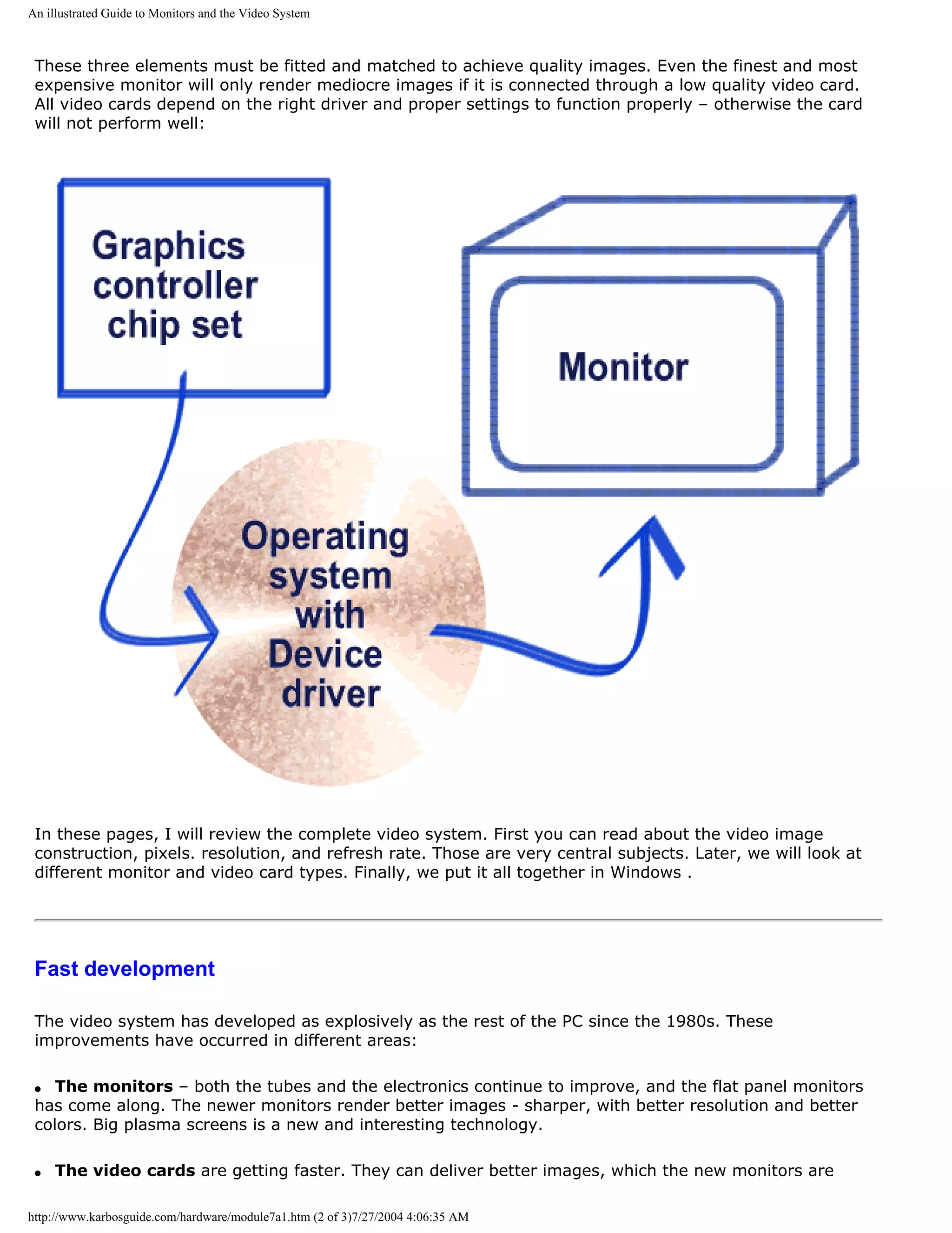
![An illustrated Guide to Monitors and the Video System
capable of producing. The user gets more tuning options. New RAM types and buses will increase speed,
and new features are added.
q Video presentation, DVD, and 3D games are other areas of development, which will change the
video card standards.
The video system is a sub system in the PC, with its own technological development. At the same time,
monitors and video cards are areas, where manufacturers and dealers often cut corners. As an ordinary
user, you can improve your screen images significantly with careful planning. That holds true when you
buy your PC - you must select your video system carefully.
It also holds true for existing video systems, where better drivers and software optimizing can help
produce the optimal screen image. We will look at that in these pages.
q Next page
q Previous page
Learn more Top
Read about video cards in Module 7b .
Read about sound cards in Module 7c .
Read about digital sound and music in Module 7d .
[Main page] [Contact] [Karbo's Dictionary] [The Software Guides]
Copyright (c) 1996-2001 by Michael B. Karbo. www.karbosguide.com.
http://www.karbosguide.com/hardware/module7a1.htm (3 of 3)7/27/2004 4:06:35 AM](https://image.slidesharecdn.com/computerhardware-michaelkarbo-121118154249-phpapp01/75/Computer-hardware-michael-karbo-149-2048.jpg)
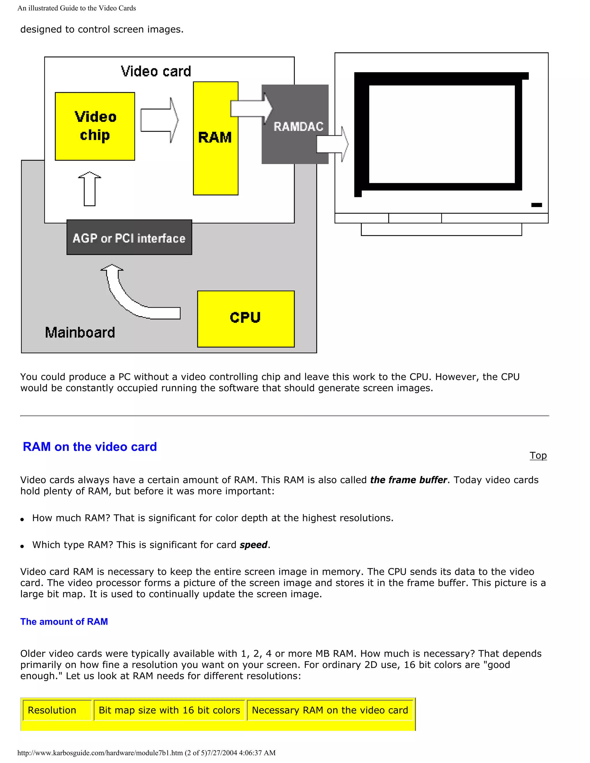
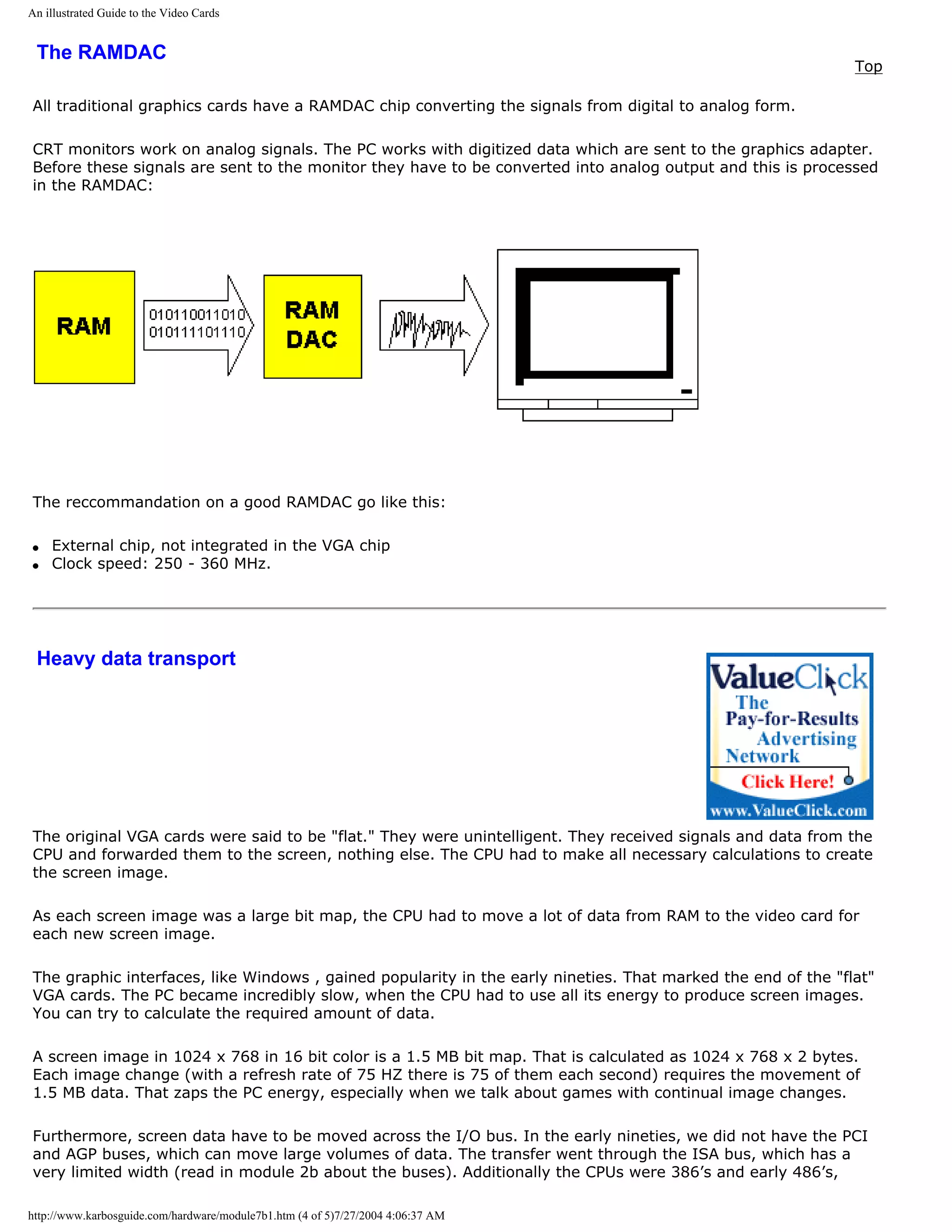
![An illustrated Guide to the Video Cards
which also had limited power.
q Next page
q Previous page
To learn more
Top
Read about monitors in Module 7a.
Read about sound cards in Module 7c .
Read about digital sound and music in Module 7d .
Read about FPU work in 3D graphics.
[Main page] [Contact] [Karbo's Dictionary] [The Software Guides]
Copyright (c) 1996-2001 by Michael B. Karbo. www.karbosguide.com.
http://www.karbosguide.com/hardware/module7b1.htm (5 of 5)7/27/2004 4:06:37 AM](https://image.slidesharecdn.com/computerhardware-michaelkarbo-121118154249-phpapp01/75/Computer-hardware-michael-karbo-154-2048.jpg)
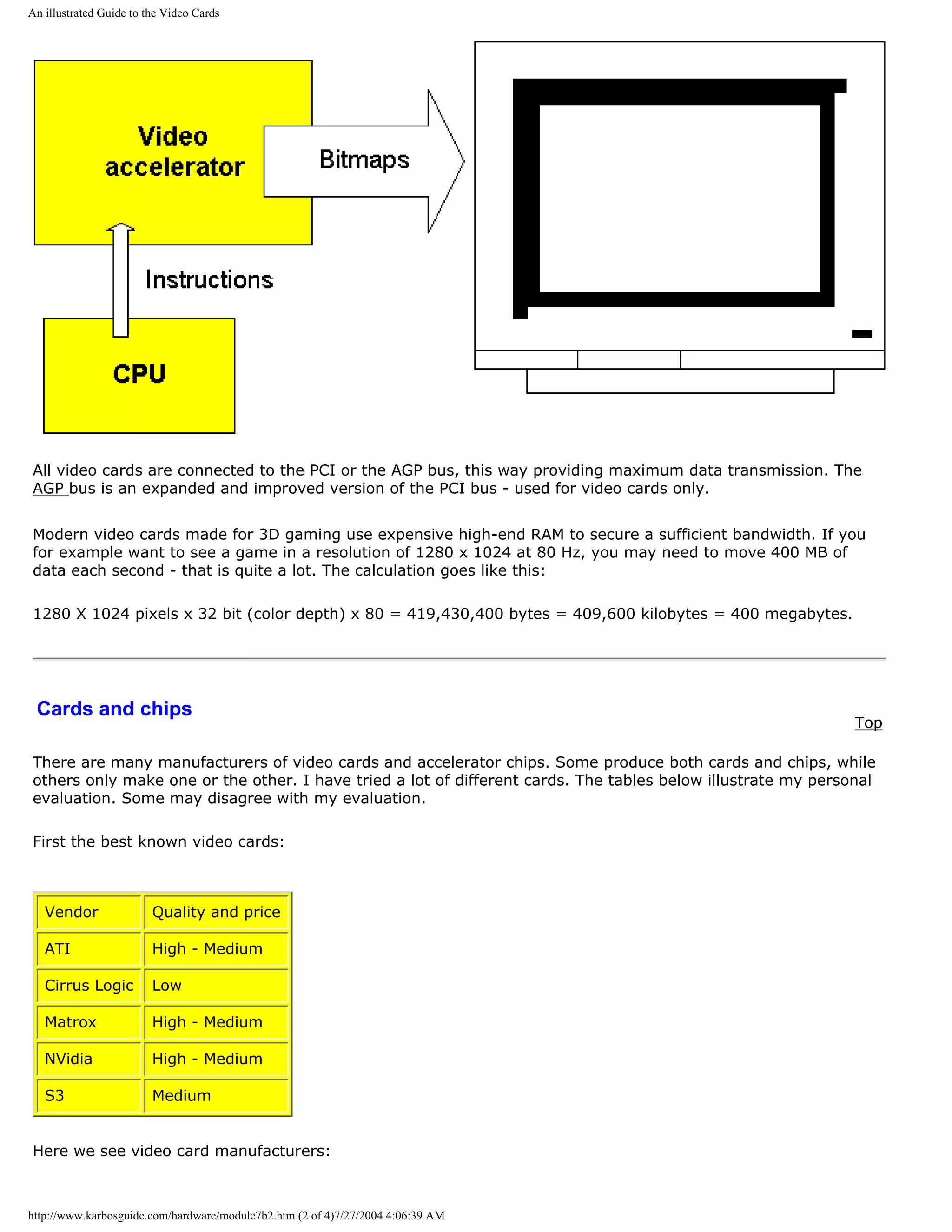
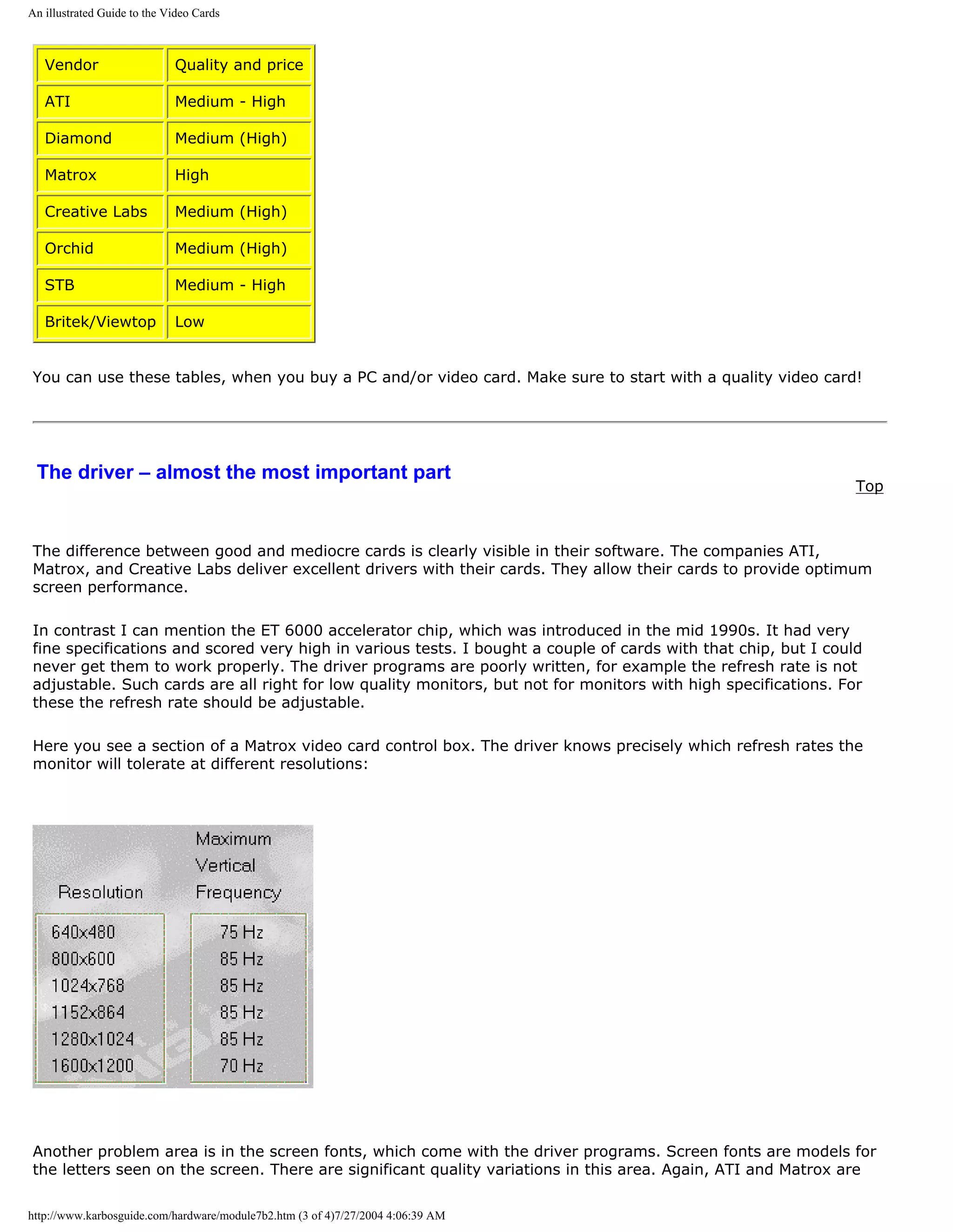
![An illustrated Guide to the Video Cards
worth mentioning.
q Next page
q Previous page
To learn more
Top
Read about video basics in Module 7a.
Read about sound cards in Module 7c .
Read about digital sound and music in Module 7d .
Read about FPU work in 3D graphics.
[Main page] [Contact] [Karbo's Dictionary] [The Software Guides]
Copyright (c) 1996-2001 by Michael B. Karbo. www.karbosguide.com.
http://www.karbosguide.com/hardware/module7b2.htm (4 of 4)7/27/2004 4:06:39 AM](https://image.slidesharecdn.com/computerhardware-michaelkarbo-121118154249-phpapp01/75/Computer-hardware-michael-karbo-158-2048.jpg)
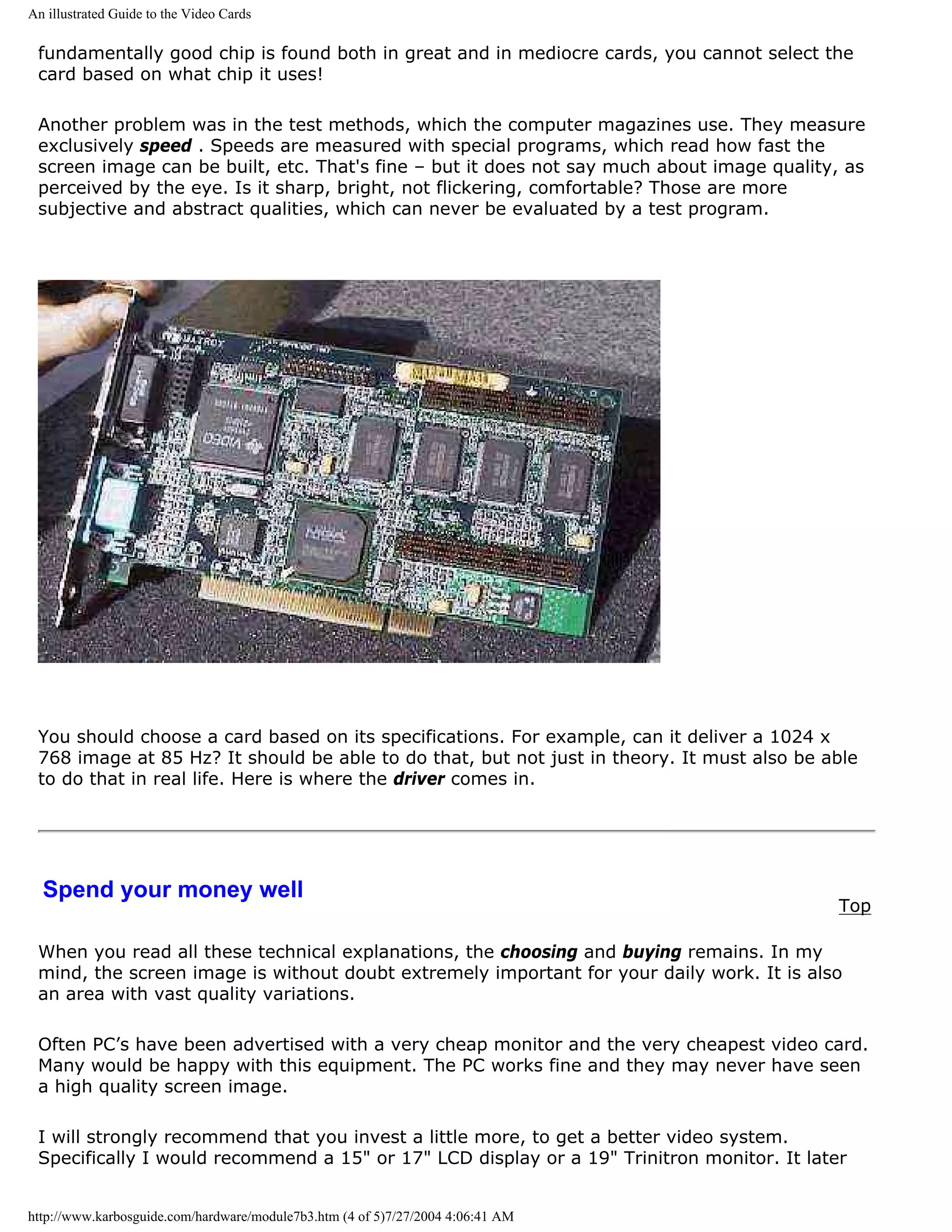
![An illustrated Guide to the Video Cards
could be a Mag or ViewSonic. Both make excellent Trinitron screens at reasonable prices.
Combine the monitor with an ATI or maybe Matrox video card and you will have a good video
system!
However, to make a good and lasting purchase, you have to understand your own video
demands. Do you need:
q Office programs with 2D graphics?
q 3D games?
q DVD acceleration?
q DVI interface?
You should get a demonstration of the card and monitor you want to buy. Especially if it is in
the low/medium price group, I will strongly recommend that you see it connected. Then
evaluate the screen image. How sharp is it? Does it flicker? Ask about resolution, color depth
and refresh rate. If the dealer cannot answer these questions, I would not trust him. Finally,
find out which driver the card needs. Read on...
q Next page
q Previous page
To learn more
Top
Read about video basics in Module 7a
Read about sound cards in Module 7c
Read about digital sound and music in Module 7d
Read about FPU work in 3D graphics
[Main page] [Contact] [Karbo's Dictionary] [The Software Guides]
Copyright (c) 1996-2001 by Michael B. Karbo. www.karbosguide.com.
http://www.karbosguide.com/hardware/module7b3.htm (5 of 5)7/27/2004 4:06:41 AM](https://image.slidesharecdn.com/computerhardware-michaelkarbo-121118154249-phpapp01/75/Computer-hardware-michael-karbo-163-2048.jpg)
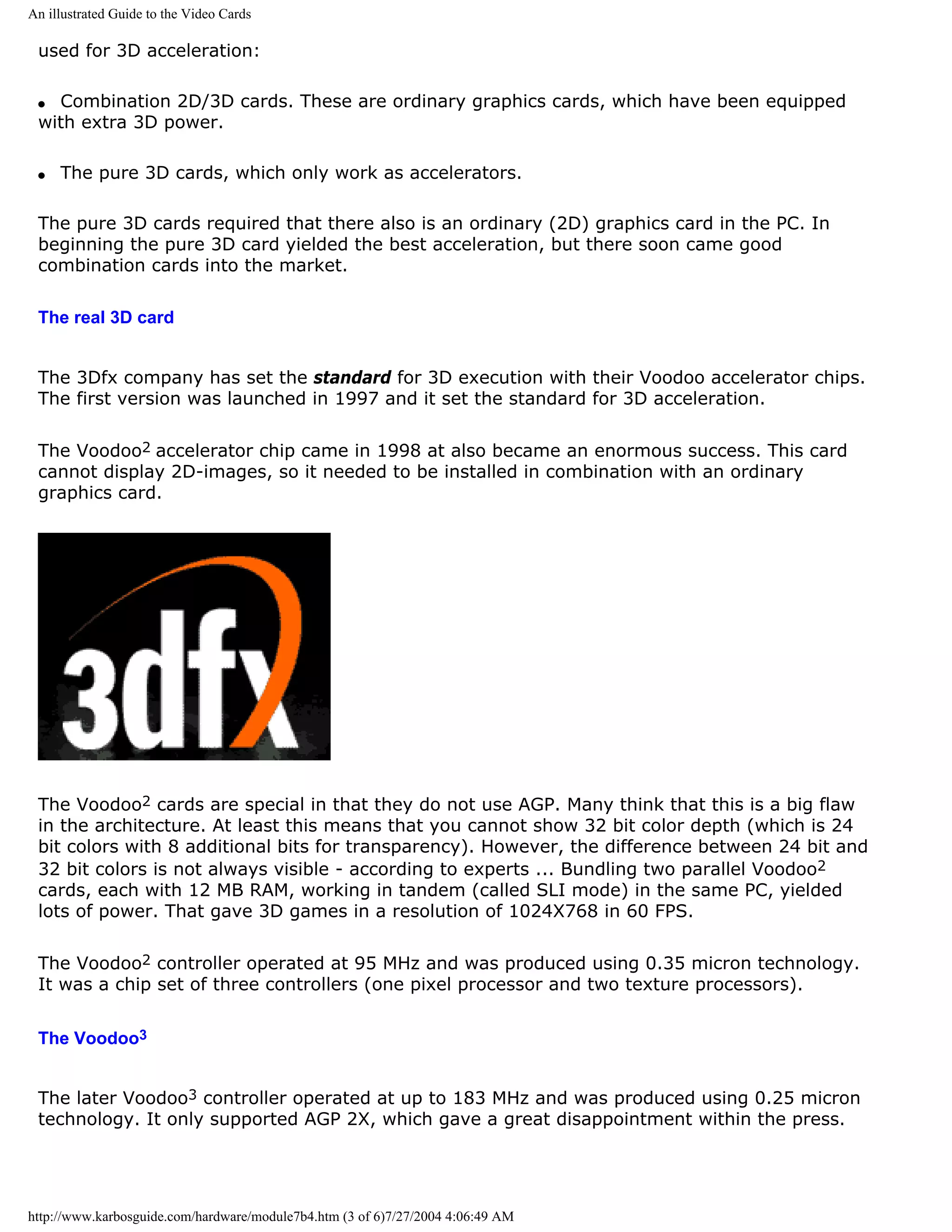
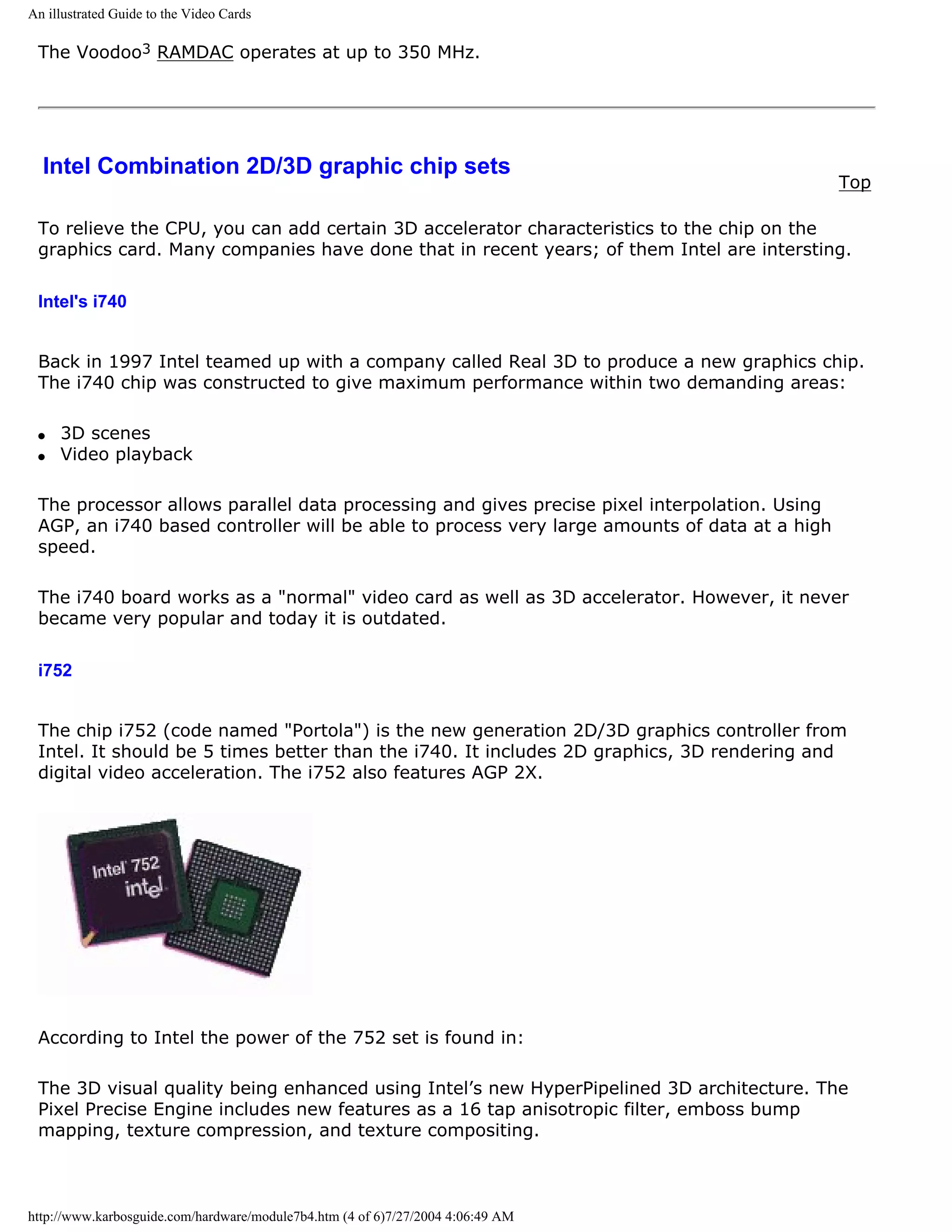
![An illustrated Guide to the Video Cards
SiS540 for AMD K6-III. These sets hold 2D/3D graphics engines as well as a lot of other
features - all in just one chip.
q On April 11, 2000 the company S3 announced that they had agreed to transfer its PC
graphics chip business to the successfull Taiwanese chip set producer VIA
q ATI's has also announced, that they are devoloping full chip sets integrated with their own
graphics controllers. We have not seen them. ATI and Matrox seems to survive in the market
by delivering high-end graphic chip sets without getting involved with the motherboard
manufactures. NVidia lives them same way serving the market for game PCs.
q Next page
q Previous page
To learn more
Top
Read about video basics in Module 7a
Read about sound cards in Module 7c
Read about digital sound and music in Module 7d
Read about FPU work in 3D graphics
[Main page] [Contact] [Karbo's Dictionary] [The Software Guides]
Copyright (c) 1996-2001 by Michael B. Karbo. www.karbosguide.com.
http://www.karbosguide.com/hardware/module7b4.htm (6 of 6)7/27/2004 4:06:49 AM](https://image.slidesharecdn.com/computerhardware-michaelkarbo-121118154249-phpapp01/75/Computer-hardware-michael-karbo-169-2048.jpg)
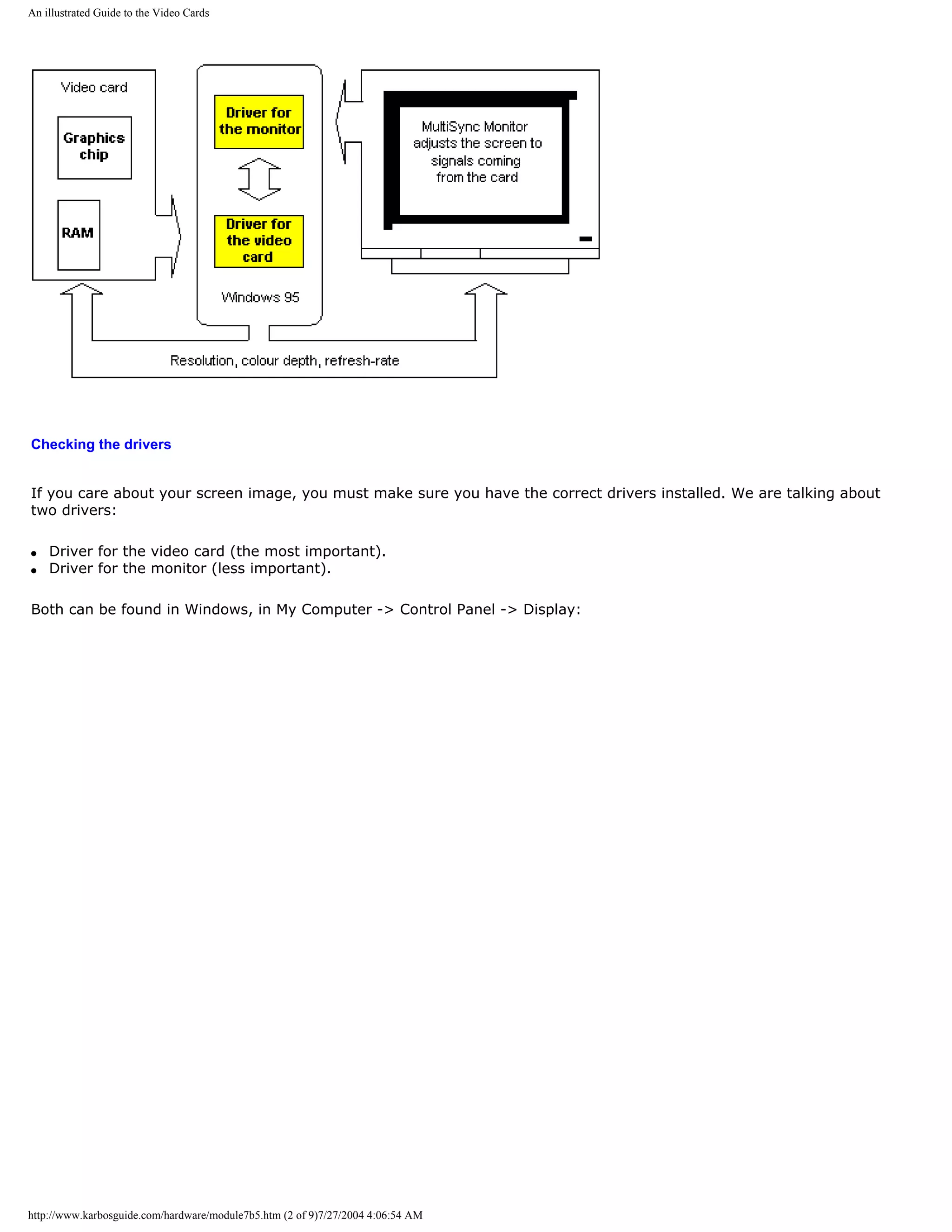
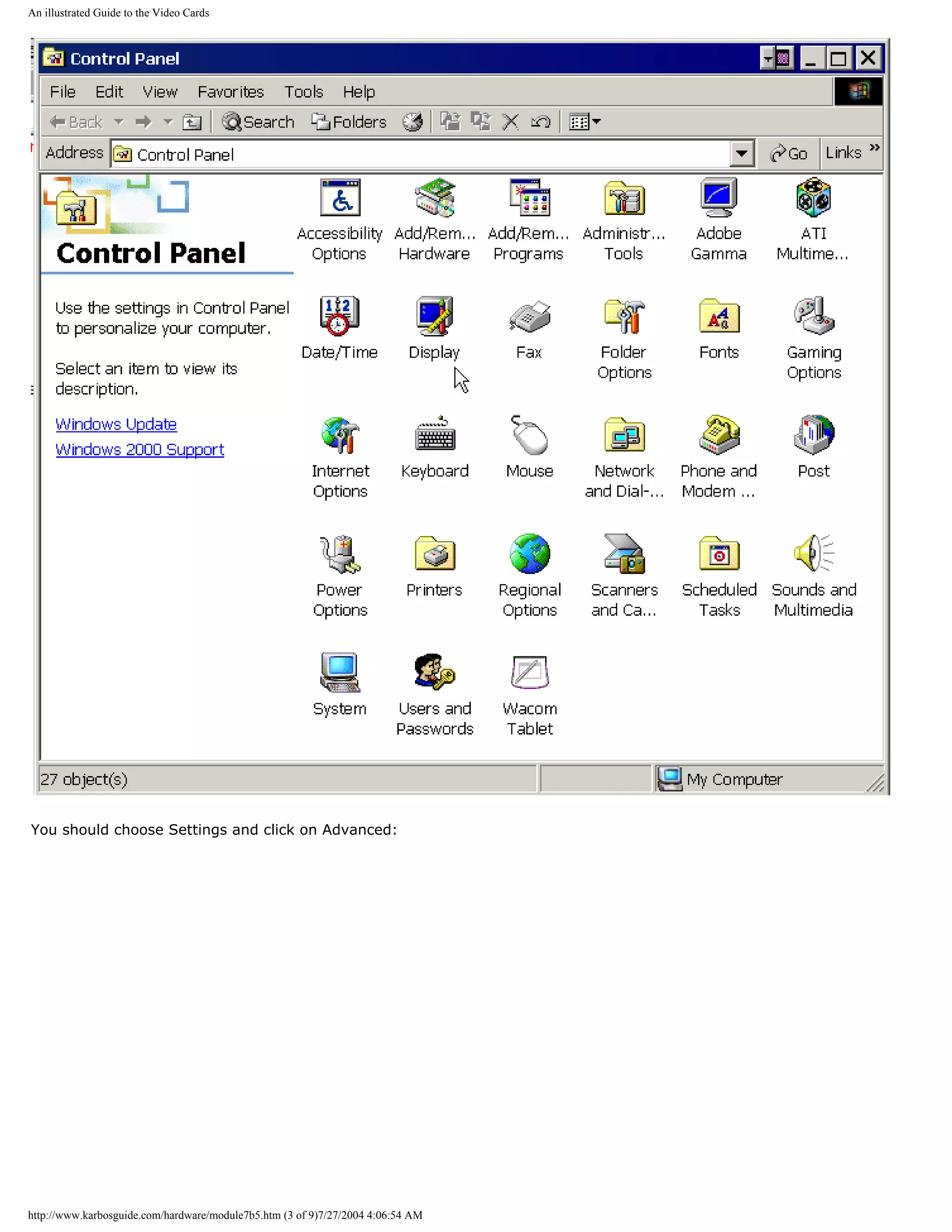
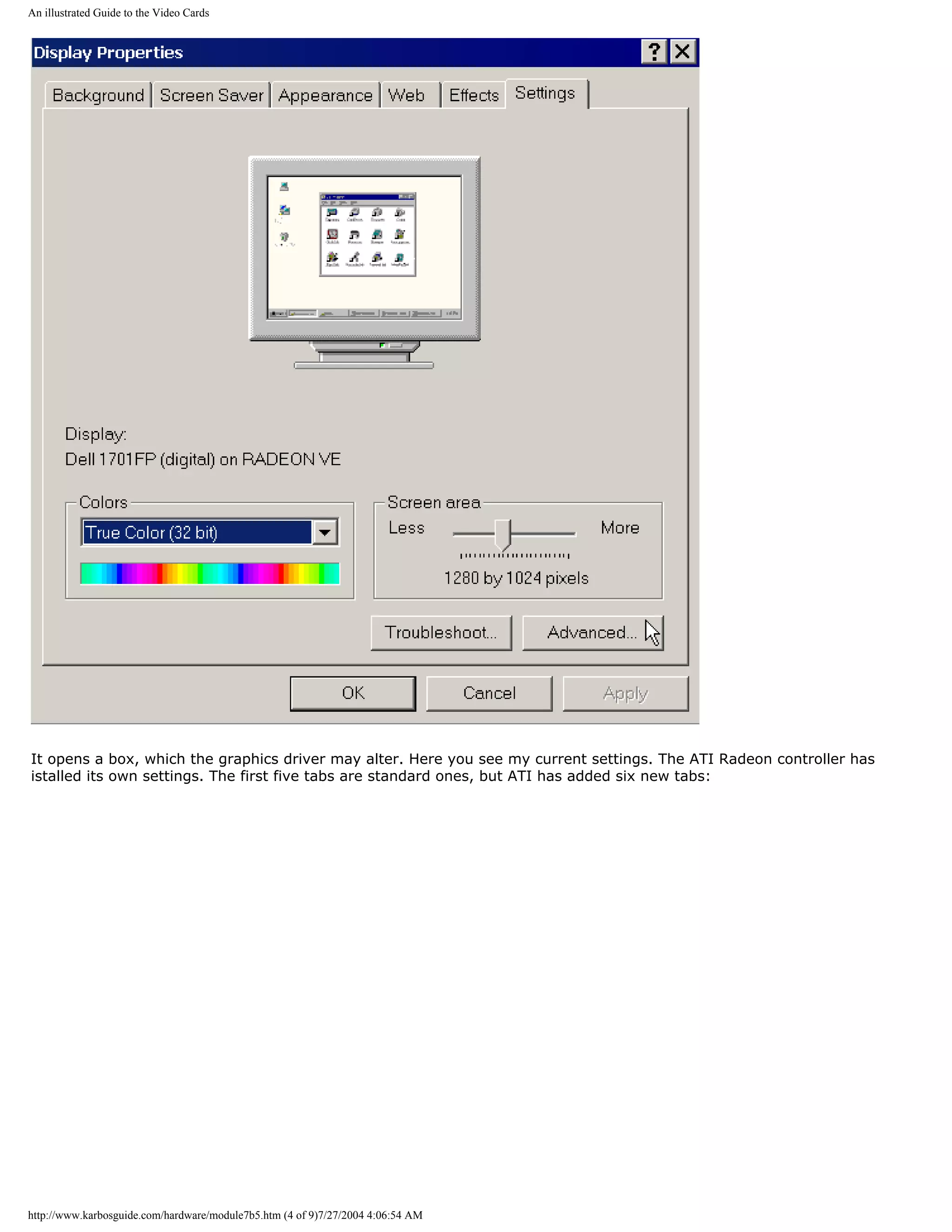
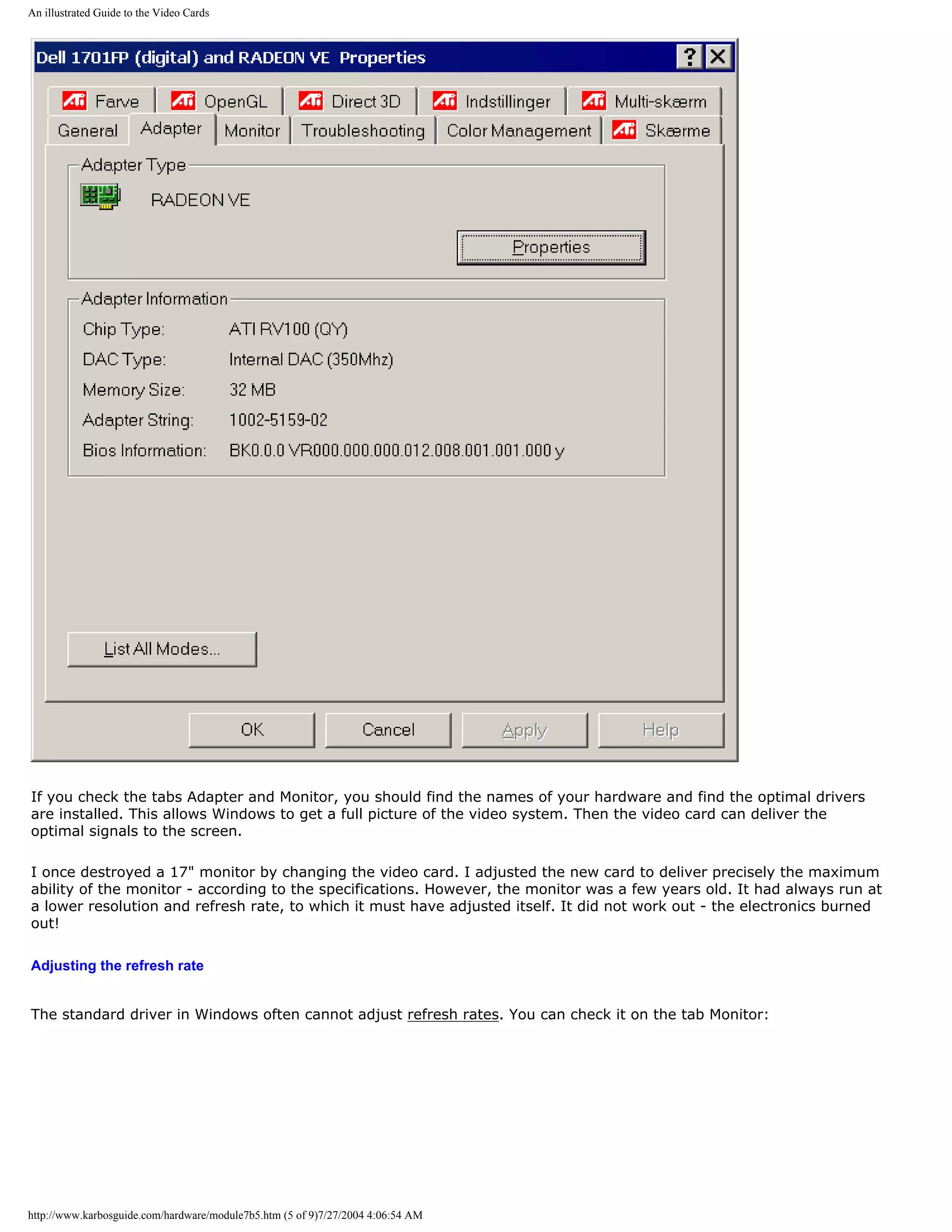
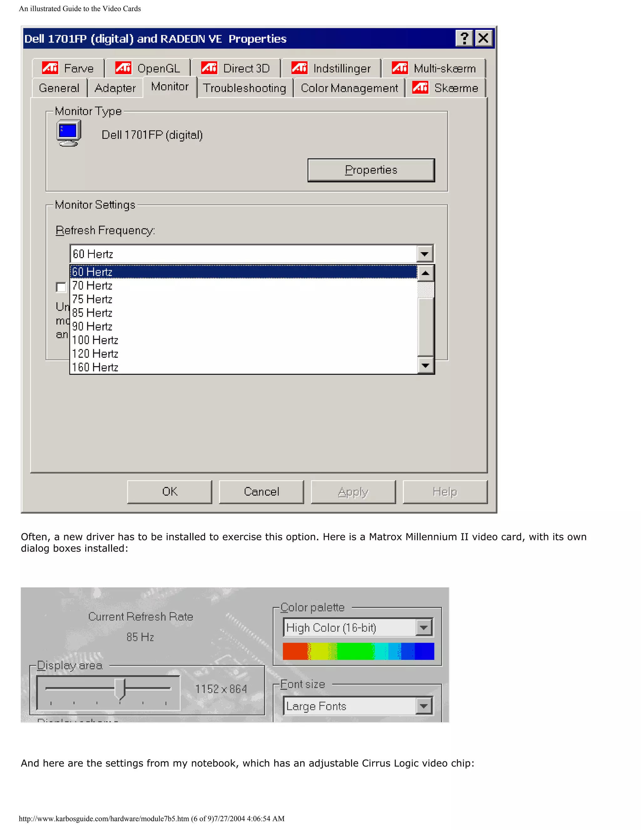
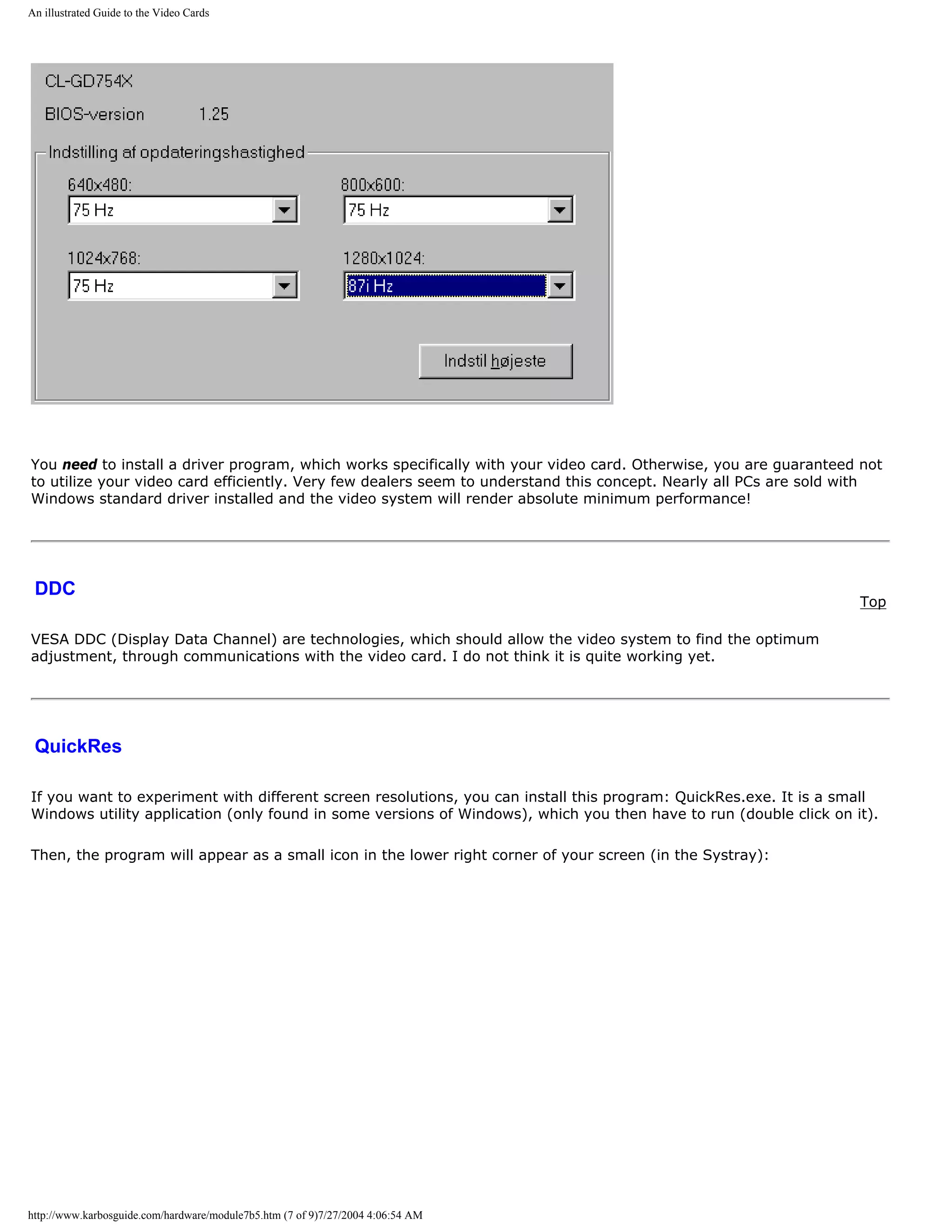
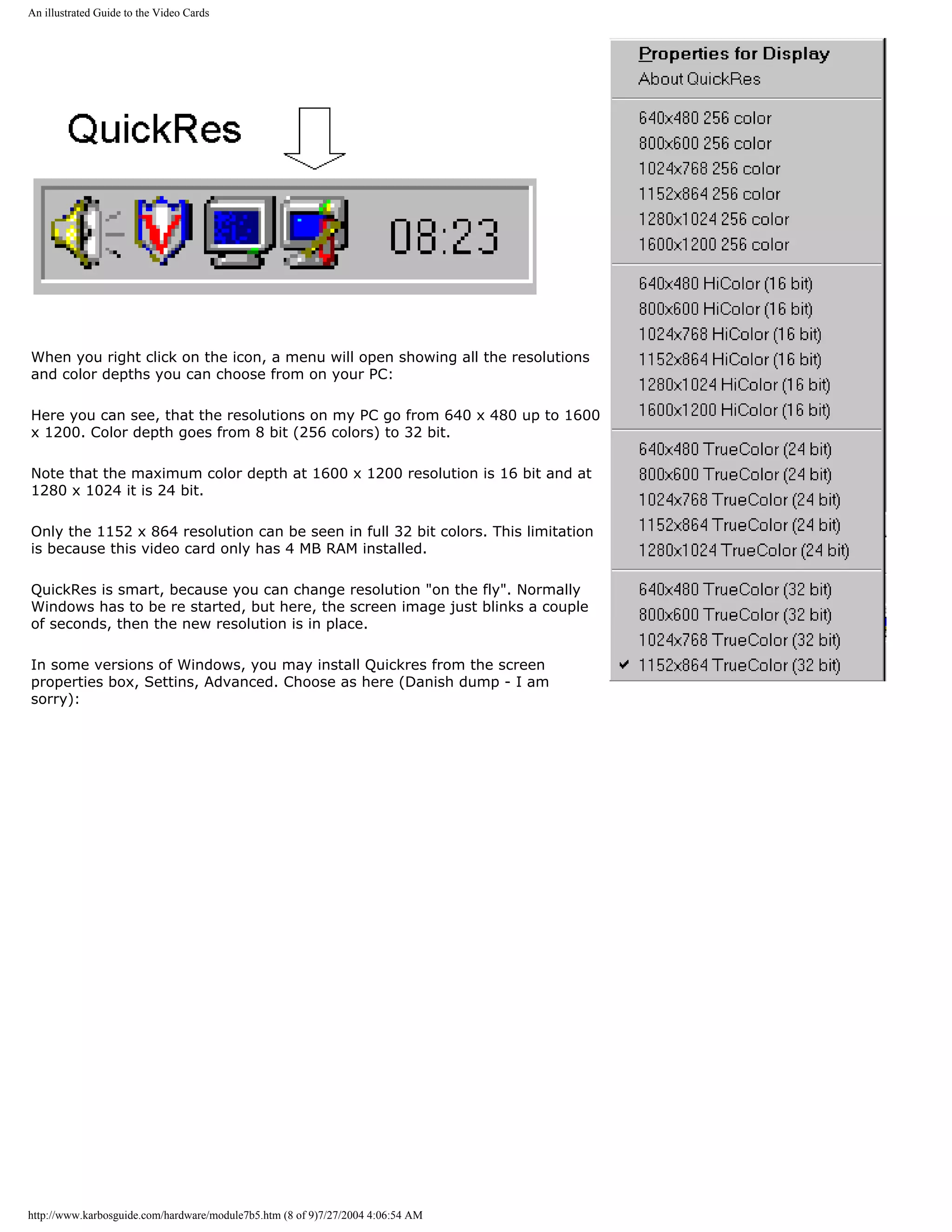
![An illustrated Guide to the Video Cards
After clicking OK the little icon is in the Systray.
q Next page
q Previous page
To learn more
Top
Read about video basics in Module 7a.
Read about digital sound and music in Module 7d .
Read about FPU work in 3D graphics.
[Main page] [Contact] [Karbo's Dictionary] [The Software Guides]
Copyright (c) 1996-2001 by Michael B. Karbo. www.karbosguide.com.
http://www.karbosguide.com/hardware/module7b5.htm (9 of 9)7/27/2004 4:06:54 AM](https://image.slidesharecdn.com/computerhardware-michaelkarbo-121118154249-phpapp01/75/Computer-hardware-michael-karbo-178-2048.jpg)
![A guide to sound cards and digital sound
Please click the banners to support our work!
KarbosGuide.com. Module 7c1.
PC sound
The contents:
q An introduction q Next page
q The synthesizer q Previous page
q The A/D conversion
q Sampling the Wav files
I do not claim to be an expert in sound cards. But I will try to describe what little I know about this
technology. The sound capabilities of the PC are quite interesting. In the late 1990s, new and radical
designs in sound technology appeared, and at the same time the MP3 wave swept the Internet society.
On the first pages we shall describe the traditional sound card concept (the Sound Blaster compatible
sound card). Then follows something on the newer technologies.
Introduction
[top]
Sound cards have a minimum of four tasks. They function as:
q Synthesizer
q MIDI interface
q Analog-to-digital conversion during the recording (A/D).
q Digital-to-analog conversion during the playback (D/A). All elements are to be explained on these
pages, so please read on.
The synthesizer
http://www.karbosguide.com/hardware/module7c1.htm (1 of 6)7/27/2004 4:06:57 AM](https://image.slidesharecdn.com/computerhardware-michaelkarbo-121118154249-phpapp01/75/Computer-hardware-michael-karbo-179-2048.jpg)
![A guide to sound cards and digital sound
The synthesizer delivers the sound. That is, the sound card generates the sounds. Here we have three
systems:
q FM synthesis, Frequency Modulation
q Wave table
q Physical modeling
FM synthesis
The cheapest sounds card use the FM technology to generate sounds simulating various instruments.
Those are true synthesizers. The sounds are synthetic – it may sound like a piano, but it is not. FM
synthesis is and sounds like the artificial sounds it consists of.
Wave tables - sampling
Wave table is the best and most expensive sound technology. This means that the sounds on the sound
card are recorded from real instruments. You record, for example, from a real piano and make a small
sample based on the recording. This sample is stored on the sound card.
When the music has to be played, you are actually listening to these samples. When they are of good
quality, the sound card can produce very impressive sounds, where the "piano" sounds like a piano.
Wave table is used in Sound Blaster's AWE card.
Physical modeling
Physical modeling synthesis is a third sound producing technology. It involves simulating sounds
through programming. The process is supposed to be rather cumbersome, but it should yield a number
of other advantages. The original Sound Blaster Gold card contains 14 instrument sounds, which are
created from physical models.
Testing the sound
The basic quality of a sound card can be tested by playing a MIDI file. Then you can easily hear the
difference. There is also a difference in how many notes (polyphony) can be played simultaneously. If
you want to compose your own music on your PC, you use the sounds available on your sound card. The
greater works you want to write, the more "voices" you will need. The SB AWE64 card has 64 voices,
while SB16 only has 20 voices.
Some sound cards can import new sounds. They are simply downloaded to the sound card, which might
have 512 KB (Sound Blaster AWE64) or 4 MB RAM (Sound Blaster AWE64 Gold) available for the user's
own sounds.
The A/D conversion
[top]
You need a A/D conversion, when analog sound signals are recorded, i.e. from a microphone. The other
way around, the D/A-converter is used when the digital sounds have to be reproduced into a signal for
the speakers amplifier.
http://www.karbosguide.com/hardware/module7c1.htm (2 of 6)7/27/2004 4:06:57 AM](https://image.slidesharecdn.com/computerhardware-michaelkarbo-121118154249-phpapp01/75/Computer-hardware-michael-karbo-180-2048.jpg)
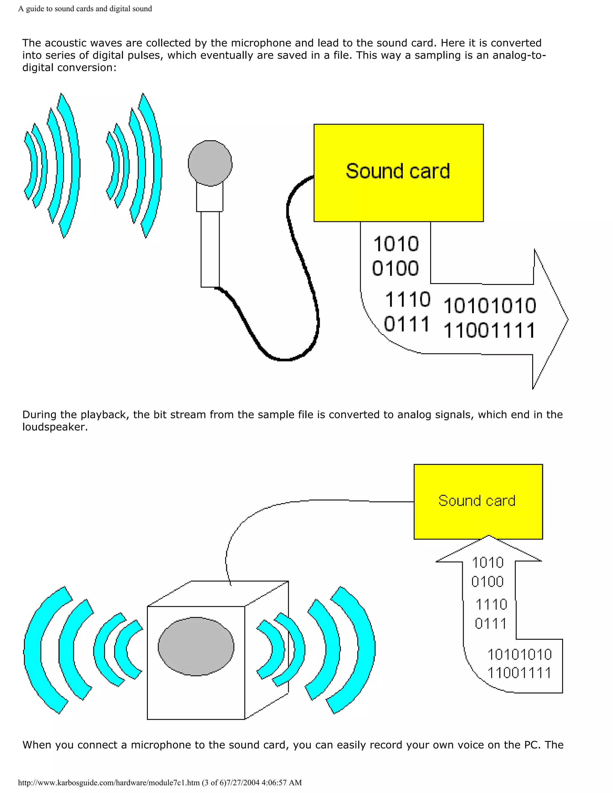
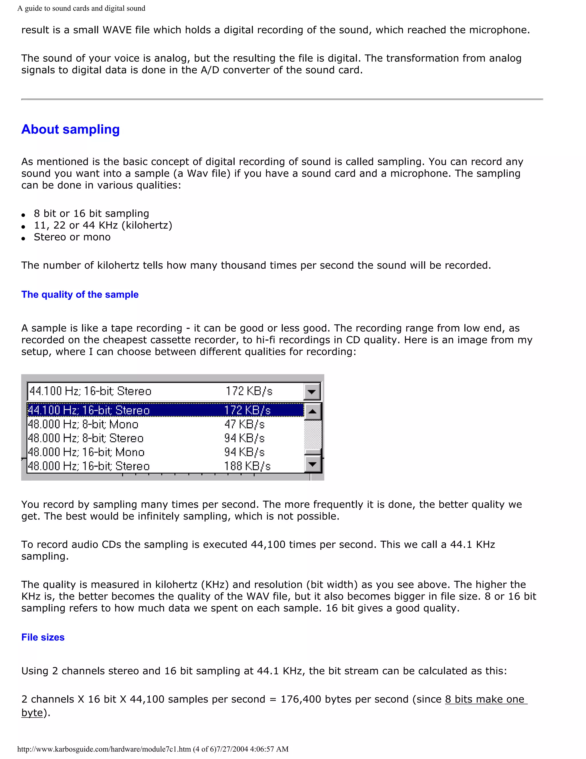
![A guide to sound cards and digital sound
This gives us the following file sizes of sampled stereo music in CD quality:
Replay Number of
bytes
One minute 10 MB
One hour 605 MB
74 Minutes 746 MB
Here you see the settings in a Wave program:
Stereo sampling at 16 bit and 44 KHz gives the best quality, but the Wave files will take up quite a bit
more space.
The Wav files
[top]
If you look down in your PC, you will find plenty of Wav files. I did a little search, and this showed up:
http://www.karbosguide.com/hardware/module7c1.htm (5 of 6)7/27/2004 4:06:57 AM](https://image.slidesharecdn.com/computerhardware-michaelkarbo-121118154249-phpapp01/75/Computer-hardware-michael-karbo-183-2048.jpg)
![A guide to sound cards and digital sound
All these Wav files contain sounds in a digital form - samples. They only contain very few seconds of
sound, because of the file size, which must not grow too big.
A Wav file will sound the same no matter which sound card you may have, be it a sound card using FM
Synthesis or Wave table. The sound is in the file and not in the sound card!
These samples above are used as sound effects within Windows. Similar samples are used as material
on music CDs and in the MOD format of digital music.
AU is another file format for samples. MP3 files are highly compressed samples.
q Next page
q Previous page
Learn more [top]
Also see: Module 7d - about digital music: MP3s, MODs etc.
Read about video cards in Module 7b .
[Main page] [Contact] [Karbo's Dictionary] [The Software Guides]
Copyright (c) 1996-2001 by Michael B. Karbo. www.karbosguide.com.
http://www.karbosguide.com/hardware/module7c1.htm (6 of 6)7/27/2004 4:06:57 AM](https://image.slidesharecdn.com/computerhardware-michaelkarbo-121118154249-phpapp01/75/Computer-hardware-michael-karbo-184-2048.jpg)
![A guide to sound cards and digital sound
Please click the banners to support our work!
KarbosGuide.com. Module 7c2.
PC sound - continued
The contents:
q The sound card - an adapter q Next page
q Newer sound cards q Previous page
The sound card - an adapter
[top]
In the previous module, we saw the principles of PC sound. Let us here look at the sound card, which is an
adapter card.
The sound card used to be a ISA card (using the old ISA interface). Here you see the original Sound Blaster
AWE64 Gold card:
http://www.karbosguide.com/hardware/module7c2.htm (1 of 4)7/27/2004 4:06:59 AM](https://image.slidesharecdn.com/computerhardware-michaelkarbo-121118154249-phpapp01/75/Computer-hardware-michael-karbo-185-2048.jpg)
![A guide to sound cards and digital sound
The connectors may look different on different sound cards, but as an example: In the back of the AWE64 Gold
card you find connectors to:
q Microphone input, a jack
q Line input, a jack
q Two phone jacks for active speakers
q A DB15 jack for MIDI or joystick.
Most sound cards typically have a 2 Watt amplifier built-in. It can push a set of earphones. An exception is the
SB Gold card, where the amplifier is eliminated. It has no practical significance, since you probably want to
attach it to a pair of active speakers.
The new sound cards
[top]
For many years PC sound has been totally dominated by the Sound Blaster card. All sound cards had to be
compatible with Sound Blaster, or it would not sell. Obviously that is due to the numerous game programs,
which require a SB compatible sound card.
The new sound cards break away from the Sound Blaster compatbility. This break involves many facets. Below
I will describe some of the tendencies in the sound technology.
Sound over the PCI bus
New sound cards use the PCI bus. The SB compatibility used to require the old ISA bus, but this has been
overcome. Creative Labs produce fine PCI-based SoundBlaster cards. With PCI you gain these advantages:
q The IRQ problems disappear.
q Signal/noise ratio can be improved with 5 dB.
q There is sufficient bandwidth (capacity for data transmission).
http://www.karbosguide.com/hardware/module7c2.htm (2 of 4)7/27/2004 4:06:59 AM](https://image.slidesharecdn.com/computerhardware-michaelkarbo-121118154249-phpapp01/75/Computer-hardware-michael-karbo-186-2048.jpg)
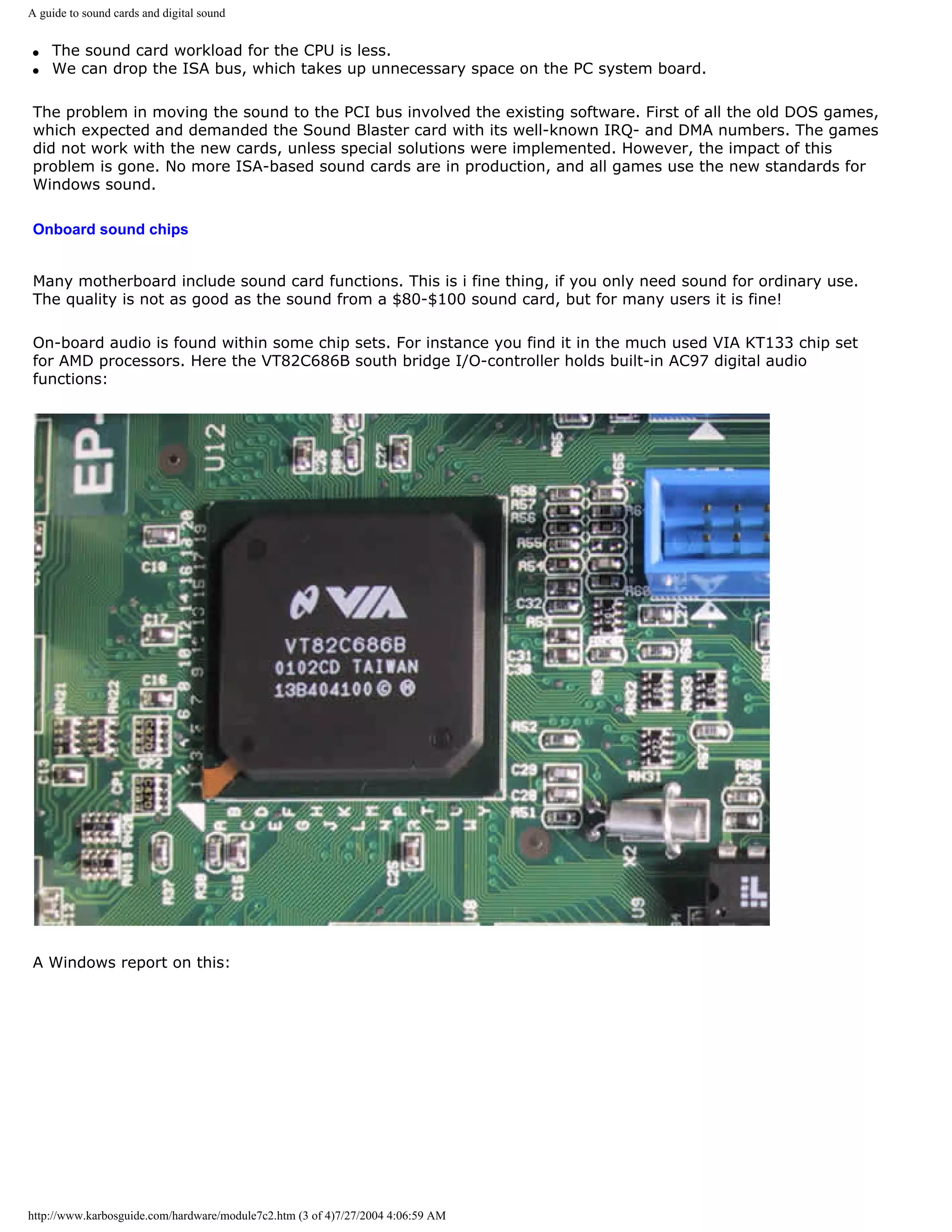
![A guide to sound cards and digital sound
Onboard sound chips is an in-expensive an simple via to incorporate sound facilities in your PC.
q Next page
q Previous page
Learn more [top]
Read Module 6a about file systems
Read about chip sets on the motherboard in module 2d
Read Module 4d about super diskette and MO drives
Read module 5a about expansion cards, where we evaluate the I/O buses from the port side
Read module 5b about AGP
Read module 7a about monitors, and 7b on graphics card
Also see: Module 7d - about digital music: MP3s, MODs etc.
[Main page] [Contact] [Karbo's Dictionary] [The Software Guides]
Copyright (c) 1996-2001 by Michael B. Karbo. www.karbosguide.com.
http://www.karbosguide.com/hardware/module7c2.htm (4 of 4)7/27/2004 4:06:59 AM](https://image.slidesharecdn.com/computerhardware-michaelkarbo-121118154249-phpapp01/75/Computer-hardware-michael-karbo-188-2048.jpg)
![A guide to sound cards and digital sound
Please click the banners to support our work!
KarbosGuide.com. Module 7c3.
PC sound - continued
The contents:
q 3D sound q Next page
q Previous page
3D sound
[top]
3D sound is a new hot area. You can create a very powerful illusion of 3D sound coming from just
loudspeaker. This is done using new 3D processors on the sound card, which work with some very
complex mathematical models. The sound comes from behind, from the front, from side to side -
completely realistic.
The idea of 3D sound has to come from games, which especially are designed for it. The sound systems
often include 4 or 6 loudspeakers. But they work fine with headphones too.
Sound Blaster Live is such a high-end, high fidelity 3D card coming from Creative Labs. It is a PCI-based
card, and the best performance comes with the Four Point Surround sound system. Diamond MX300 is
another.
SB Live!
The SoundBlaster top model sound card is called SoundBlaster Live!
It includes a lot of fine and powerful features:
q EMU10K1 accelerator chip
http://www.karbosguide.com/hardware/module7c3.htm (1 of 4)7/27/2004 4:07:01 AM](https://image.slidesharecdn.com/computerhardware-michaelkarbo-121118154249-phpapp01/75/Computer-hardware-michael-karbo-189-2048.jpg)
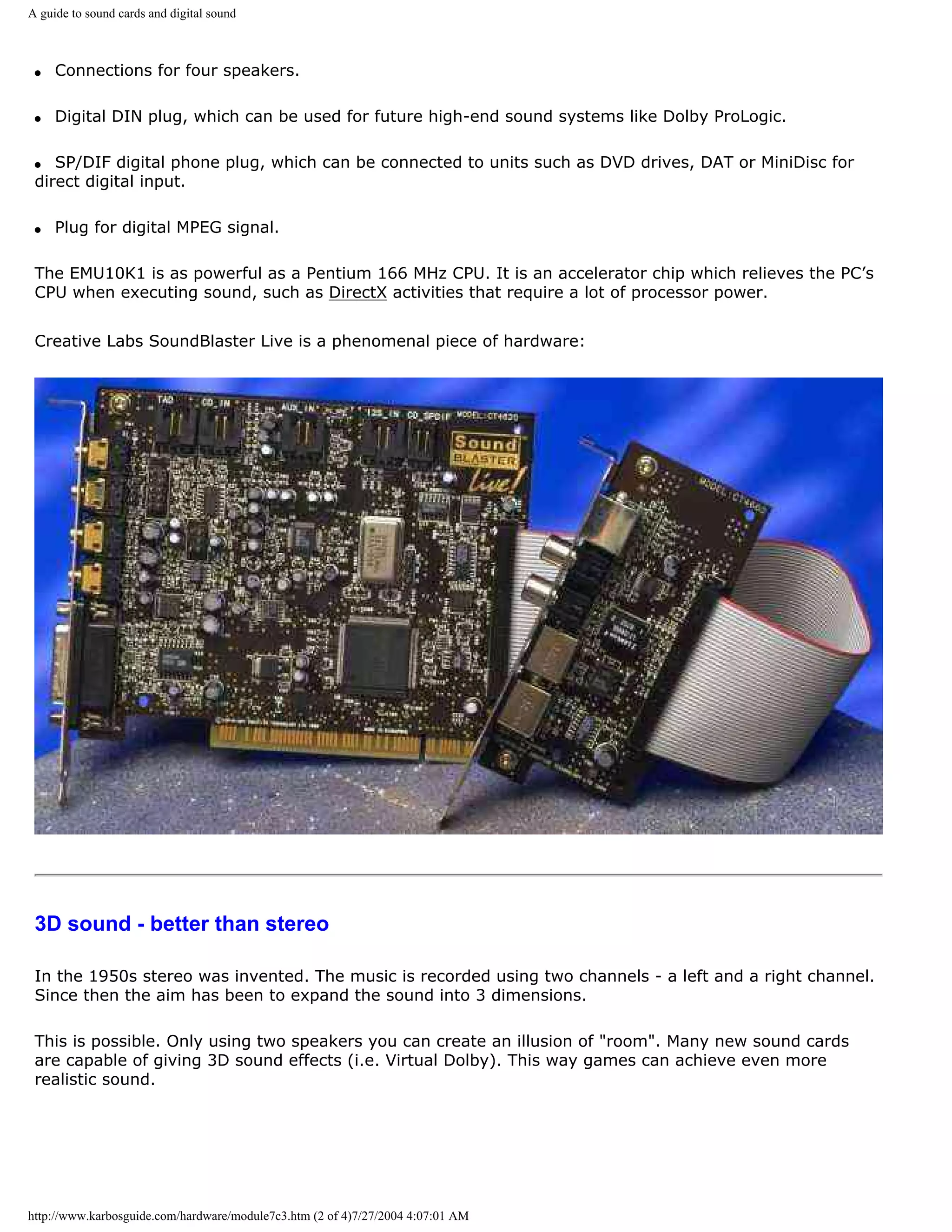
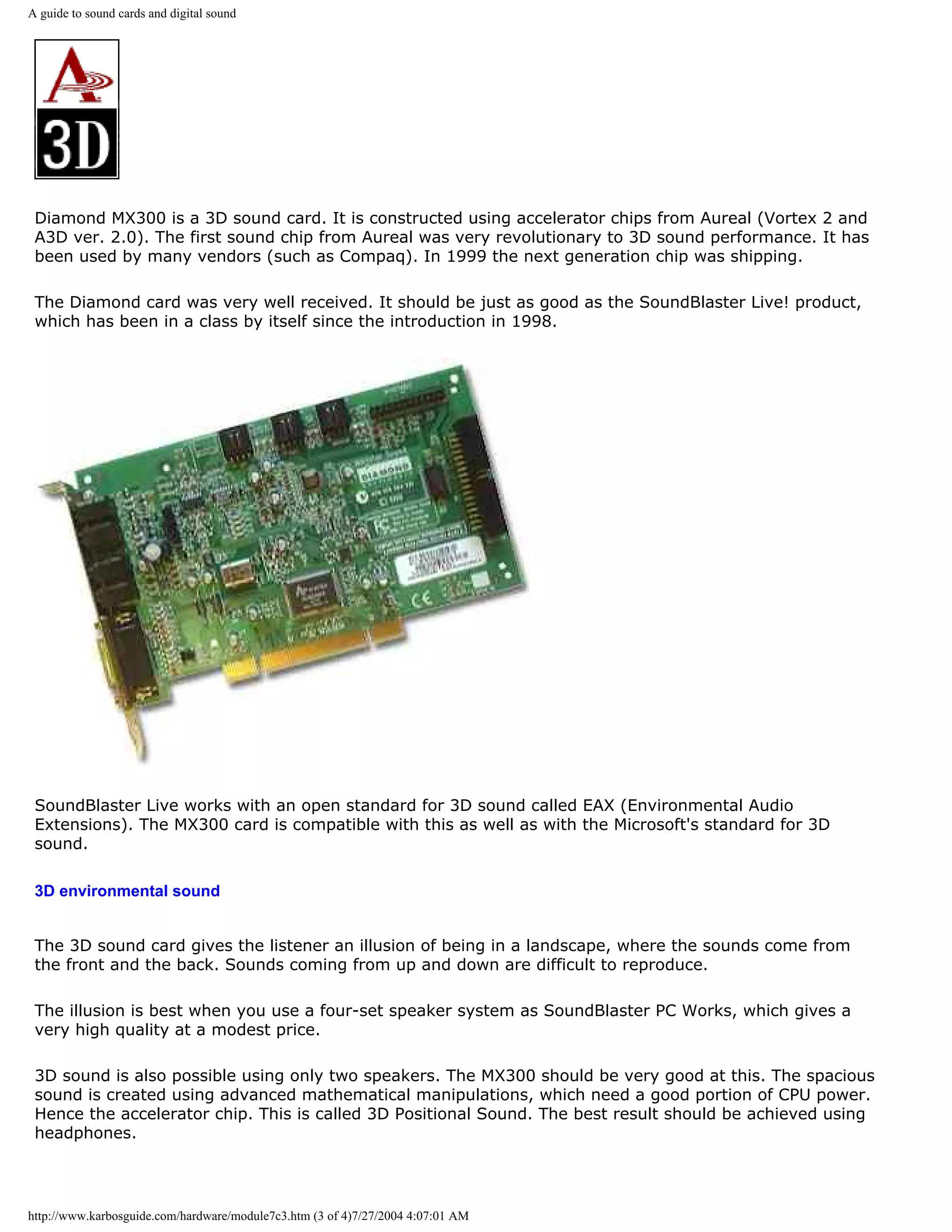
![A guide to sound cards and digital sound
Another 3D effect is called Environmental Sound. Here the sound from a game is changed corresponding
to the physical situation of the characters. If a person enters a tunnel, there may be an echo. In a big
empty hall the sound is completely different. This way the games can send commands to the sound
card, which adjust the feeling of the sound to the environment.
q Next page
q Previous page
Learn more
[top]
Read Module 6a about file systems
Read about chip sets on the motherboard in module 2d
Read Module 4d about super diskette and MO drives
Read module 5a about expansion cards, where we evaluate the I/O buses from the port side
Read module 5b about AGP
Read module 7a about monitors, and 7b on graphics card
Also see: Module 7d - about digital music: MP3s, MODs etc.
[Main page] [Contact] [Karbo's Dictionary] [The Software Guides]
Copyright (c) 1996-2001 by Michael B. Karbo. www.karbosguide.com.
http://www.karbosguide.com/hardware/module7c3.htm (4 of 4)7/27/2004 4:07:01 AM](https://image.slidesharecdn.com/computerhardware-michaelkarbo-121118154249-phpapp01/75/Computer-hardware-michael-karbo-192-2048.jpg)
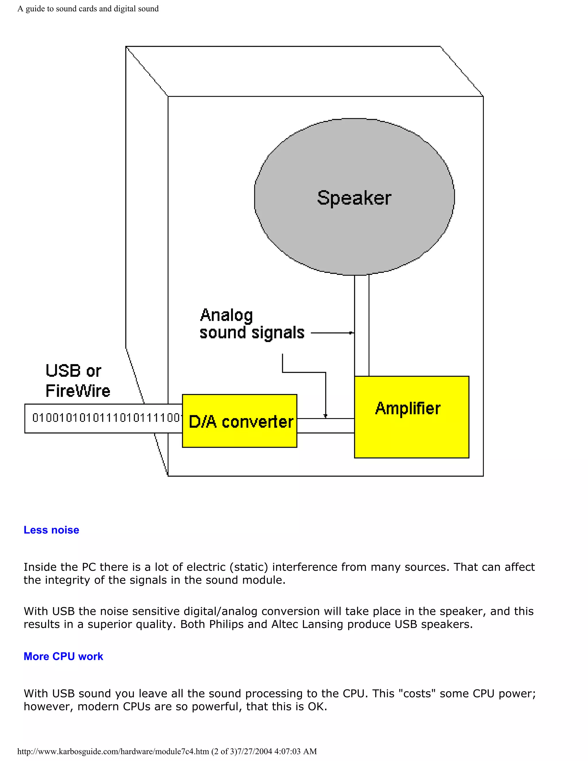
![A guide to sound cards and digital sound
You find high fidelity loudspeakers with built-in amplifier and converter, which can receive
pure digital signals (via USB). One could hope, that these speakers will be able to interpret
data from hi-fi equipment, PC, TV/video and other sources. See the description of some of
the finest speakers I ever have heard: A set ofPhilips USB speakers.
q Next page
q Previous page
Learn more [top]
Also see: Module 7d - about digital music: MP3s, MODs etc.
[Main page] [Contact] [Karbo's Dictionary] [The Software Guides]
Copyright (c) 1996-2001 by Michael B. Karbo. www.karbosguide.com.
http://www.karbosguide.com/hardware/module7c4.htm (3 of 3)7/27/2004 4:07:03 AM](https://image.slidesharecdn.com/computerhardware-michaelkarbo-121118154249-phpapp01/75/Computer-hardware-michael-karbo-195-2048.jpg)
![A guide to sound cards and digital sound
Please click the banners to support our work!
KarbosGuide.com. Module 7c5.
PC sound - continued
The contents:
q DOS or DirectX q Next page
q Previous page
DOS or DirectX
[top]
When so many games used to be DOS based, it primarily was because of the sound. Under
DOS the programmer can modify and manipulate the sound card to a very high extent. It can
be controlled very precisely, sounds can be mixed without interruption, and all kinds of
effects can be designed. Here DOS proves very effective - the operating system permits
direct control of the hardware.
The disadvantage with DOS sound is, that the hardware must be totally standardized. This
gave the Sound Blaster card its great success.
Windows
In Windows all program instructions to hardware are executed through a programming layer
http://www.karbosguide.com/hardware/module7c5.htm (1 of 3)7/27/2004 4:07:04 AM](https://image.slidesharecdn.com/computerhardware-michaelkarbo-121118154249-phpapp01/75/Computer-hardware-michael-karbo-196-2048.jpg)
![A guide to sound cards and digital sound
(API).
The first multimedia API would not allow mixing of sounds. Therefore the music in the
Windows-based game had to be cut off, if there was a need for playing such a thing as the
sound of an explosion. This put heavy restraints on programming creativity. Consequently
DOS based game applications remained long into the Windows era. But it changed ...
DirectX
DirectX is a set of multimedia APIs ( application program interface ) developed for Windows .
It is a collection of programs which enable much improved low level control over the
hardware in games and other multimedia applications. DirectX has now reached version 6.1
and includes:
q DirectDraw
q DirectSound
q DiectSound3D
q DirectPlay
q DirectInput
q DirectSetup
These programs are designed to enable all possible image and sound effects.
The advantage of DirectX is that the applications can be written directly to Windows and
simultaneously get maximum hardware control. Hence DirectX is very important to hardware
manufactures. To make sure that the new products work together with all software, the
drivers have support the latest version of DirectX.
With DirectX we should finally have eliminated the need for programs to rely on Sound
Blaster compatibility.
DirectX comes in new versions every year.
In version 7.0 you find improved 3D acceleration of sound as well as picture with reduced
CPU usage. The performance should be increased with 20% compared to version 6.1.
Windows 2000 was the first NT-based version of Windows to include DirectX.
q Next page
q Previous page
Learn more [top]
http://www.karbosguide.com/hardware/module7c5.htm (2 of 3)7/27/2004 4:07:04 AM](https://image.slidesharecdn.com/computerhardware-michaelkarbo-121118154249-phpapp01/75/Computer-hardware-michael-karbo-197-2048.jpg)
![A guide to sound cards and digital sound
Also see: Module 7d - about digital music: MP3s, MODs etc.
[Main page] [Contact] [Karbo's Dictionary] [The Software Guides]
Copyright (c) 1996-2001 by Michael B. Karbo. www.karbosguide.com.
http://www.karbosguide.com/hardware/module7c5.htm (3 of 3)7/27/2004 4:07:04 AM](https://image.slidesharecdn.com/computerhardware-michaelkarbo-121118154249-phpapp01/75/Computer-hardware-michael-karbo-198-2048.jpg)
![A guide to digital music #1
KarbosGuide.com. Module 7d1.
About digital music
The contents:
There are quite a few different kinds of music formats you can q Next page
find on the Internet. A few of them are described on these pages. q Previous page
q About the player
About the player
[top]
When you have some of those files, you need a player (a plugin) to replay it on your PC. All
versions of Windows have built-in players for the Wav and Midi files, so you do not have to
think of that. Just double-click on the file, and the sound or tune is replayed:
However, the sound files MP3s and the MODs are much more interesting formats than Wav
http://www.karbosguide.com/hardware/module7d1.htm (1 of 2)7/27/2004 4:07:06 AM](https://image.slidesharecdn.com/computerhardware-michaelkarbo-121118154249-phpapp01/75/Computer-hardware-michael-karbo-199-2048.jpg)
![A guide to digital music #1
and Midi. But you need plugins, a little program to replay the tunes. These players are freely
available on the Internet - I'll give you the links later.
Some players are only available as plugins to browsers. This goes for the Koan stuff. Others
(MP3s and MODs) can be achieved as stand-alone players or plugins.
q Next page
q Previous page
Learn more [top]
q Click for Module 3b about CPU improvements
Click for Module 3c about the 5th generations CPUs (Pentiums etc.)
Click for Module 3d about the clock frequencies
Click for Module 3e about 6th generations CPUs (Pentium IIs etc.)
[Main page] [Contact] [Karbo's Dictionary] [The Software Guides]
Copyright (c) 1996-2001 by Michael B. Karbo. www.karbosguide.com.
http://www.karbosguide.com/hardware/module7d1.htm (2 of 2)7/27/2004 4:07:06 AM](https://image.slidesharecdn.com/computerhardware-michaelkarbo-121118154249-phpapp01/75/Computer-hardware-michael-karbo-200-2048.jpg)
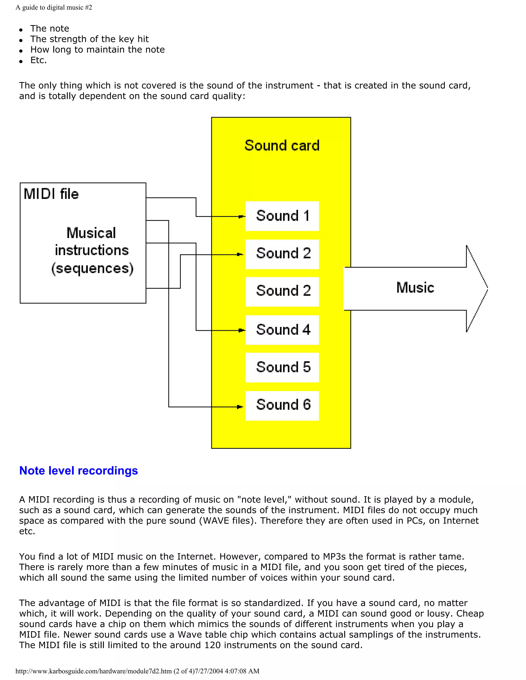
![A guide to digital music #2
MIDI interface for keyboards
[top]
A musical keyboard can be connected to the sound card with a connector. That is called a MIDI
interface. You can buy special PC musical keyboards, or you can use one of the keyboards which are
available in music stores. It will work as long as the MIDI connectors match.
You connect your DIN connector to the piano keyboard. In the other end of the cable is a DB15
connector to the sound card. Then you can play from the piano keyboard through the sound card. Of
course it requires a program which can handle music, but it works.
I have tried it myself. The Sound Blaster AWE64 Gold comes with the program Cubasis. Once I
connected an old and cheap piano keyboard (with built-in rhythm box) to the sound card, and
everything worked through Cubasis. The keyboard acted as a "Local Synthesizer" in the program
settings.
This keyboard is especially designed for the PC.
Links
[top]
Here is a link to Anselmo Salzani, who tries to create exciting music in the MIDI format. His page also
includes a lot of other interesting music links: Brazilian MIDI music.
And a Dane: Anders Kornerups MIDI music
http://www.karbosguide.com/hardware/module7d2.htm (3 of 4)7/27/2004 4:07:08 AM](https://image.slidesharecdn.com/computerhardware-michaelkarbo-121118154249-phpapp01/75/Computer-hardware-michael-karbo-203-2048.jpg)
![A guide to digital music #2
q Next page
q Previous page
Learn more [top]
Click for Module 3b about CPU improvements
Click for Module 3c about the 5th generations CPUs (Pentiums etc.)
Click for Module 3d about the clock frequencies
Click for Module 3e about 6th generations CPUs (Pentium IIs etc.)
[Main page] [Contact] [Karbo's Dictionary] [The Software Guides]
Copyright (c) 1996-2001 by Michael B. Karbo. www.karbosguide.com.
http://www.karbosguide.com/hardware/module7d2.htm (4 of 4)7/27/2004 4:07:08 AM](https://image.slidesharecdn.com/computerhardware-michaelkarbo-121118154249-phpapp01/75/Computer-hardware-michael-karbo-204-2048.jpg)
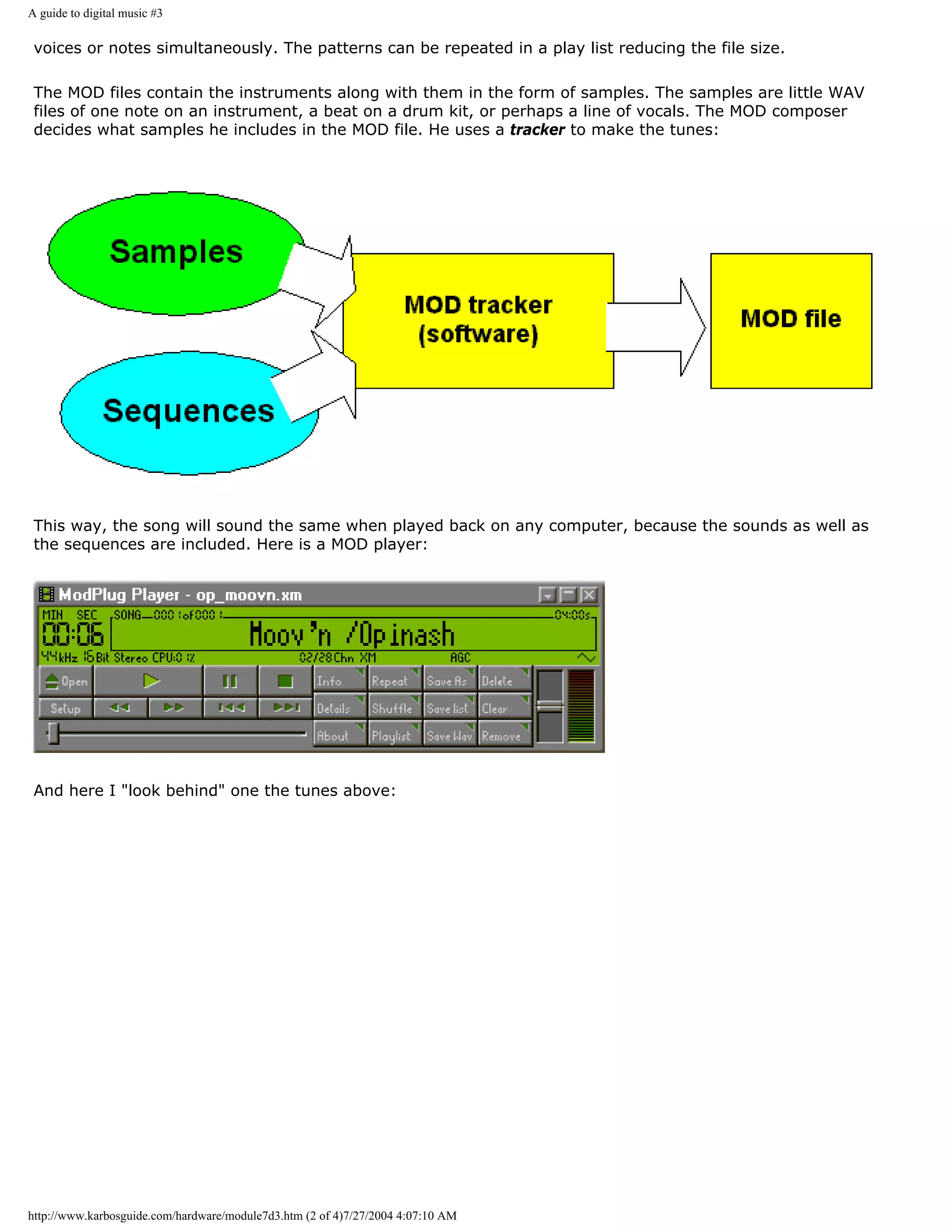
![A guide to digital music #3
You can download great music in the MOD format. The files are named .MOD or .XM. The most incredible is
the file size. There obviously is a lot of compression in it, often you get more than a minute high quality
replay out of a MOD file of just 100 KB.
All you need is a little software:
Links
[top]
Visit this MOD site where you find players and other MOD stuff.
Also check Great Swedish music in MOD format.
q Next page
http://www.karbosguide.com/hardware/module7d3.htm (3 of 4)7/27/2004 4:07:10 AM](https://image.slidesharecdn.com/computerhardware-michaelkarbo-121118154249-phpapp01/75/Computer-hardware-michael-karbo-207-2048.jpg)
![A guide to digital music #3
q Previous page
Learn more [top]
Click for Module 3b about CPU improvements
Click for Module 3c about the 5th generations CPUs (Pentiums etc.)
Click for Module 3d about the clock frequencies
Click for Module 3e about 6th generations CPUs (Pentium IIs etc.)
[Main page] [Contact] [Karbo's Dictionary] [The Software Guides]
Copyright (c) 1996-2001 by Michael B. Karbo. www.karbosguide.com.
http://www.karbosguide.com/hardware/module7d3.htm (4 of 4)7/27/2004 4:07:10 AM](https://image.slidesharecdn.com/computerhardware-michaelkarbo-121118154249-phpapp01/75/Computer-hardware-michael-karbo-208-2048.jpg)
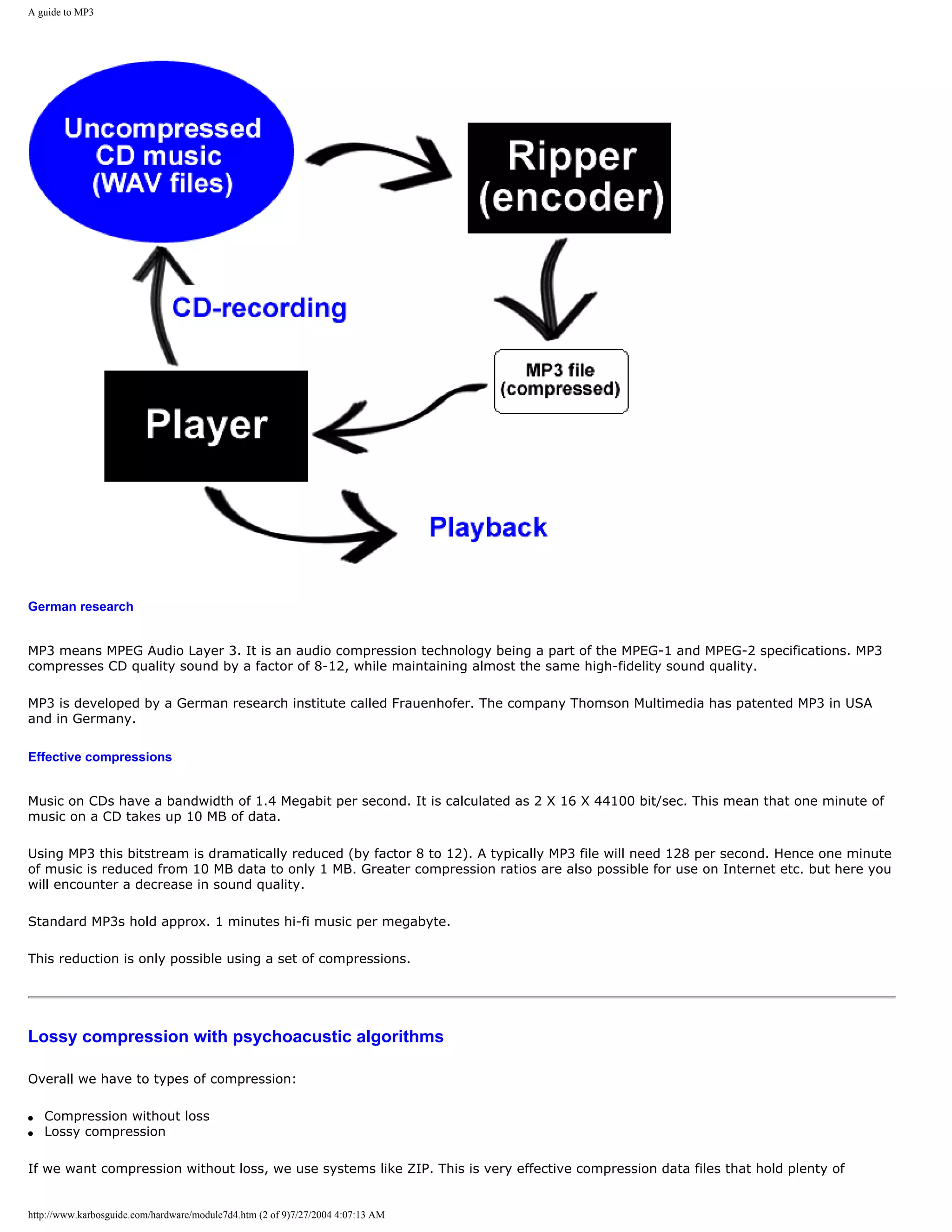
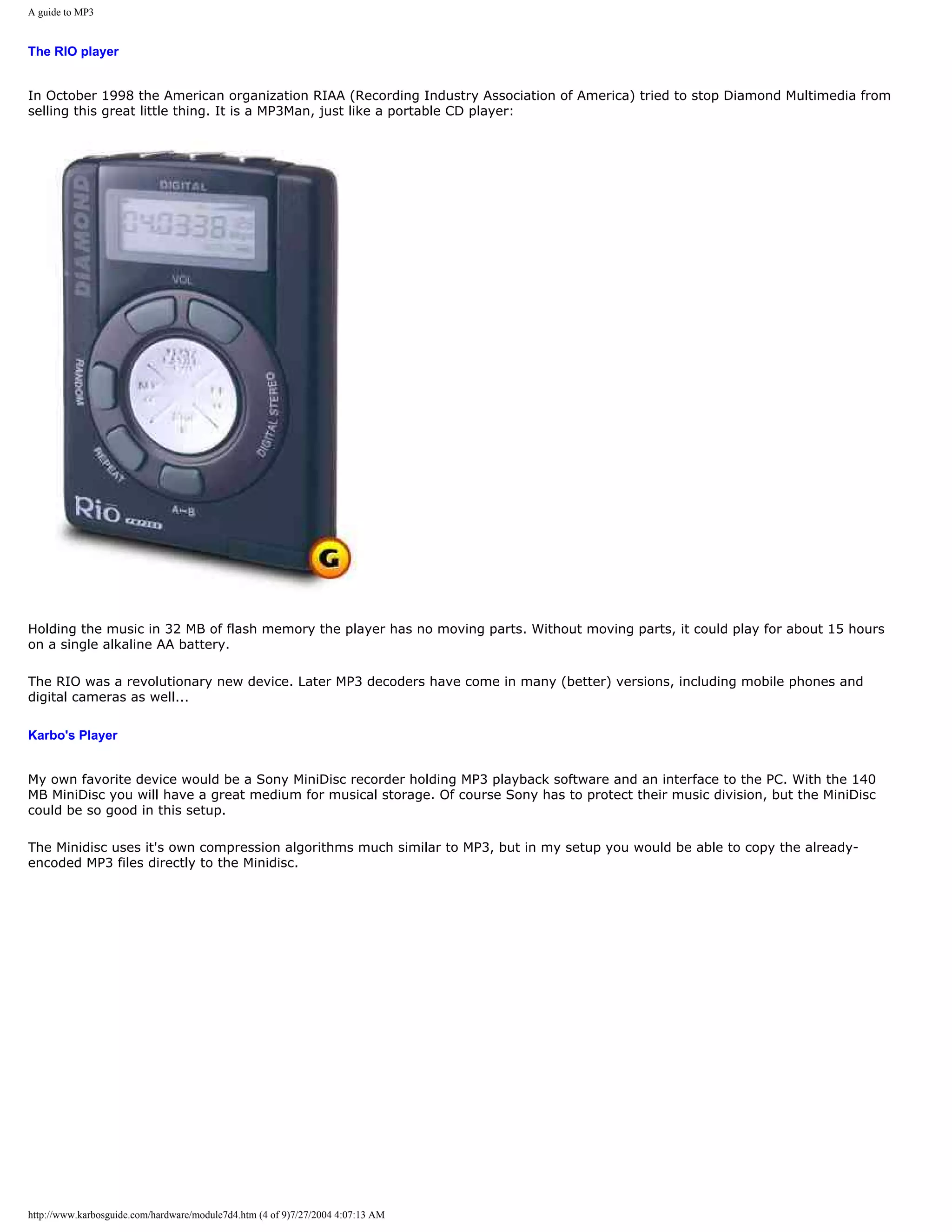
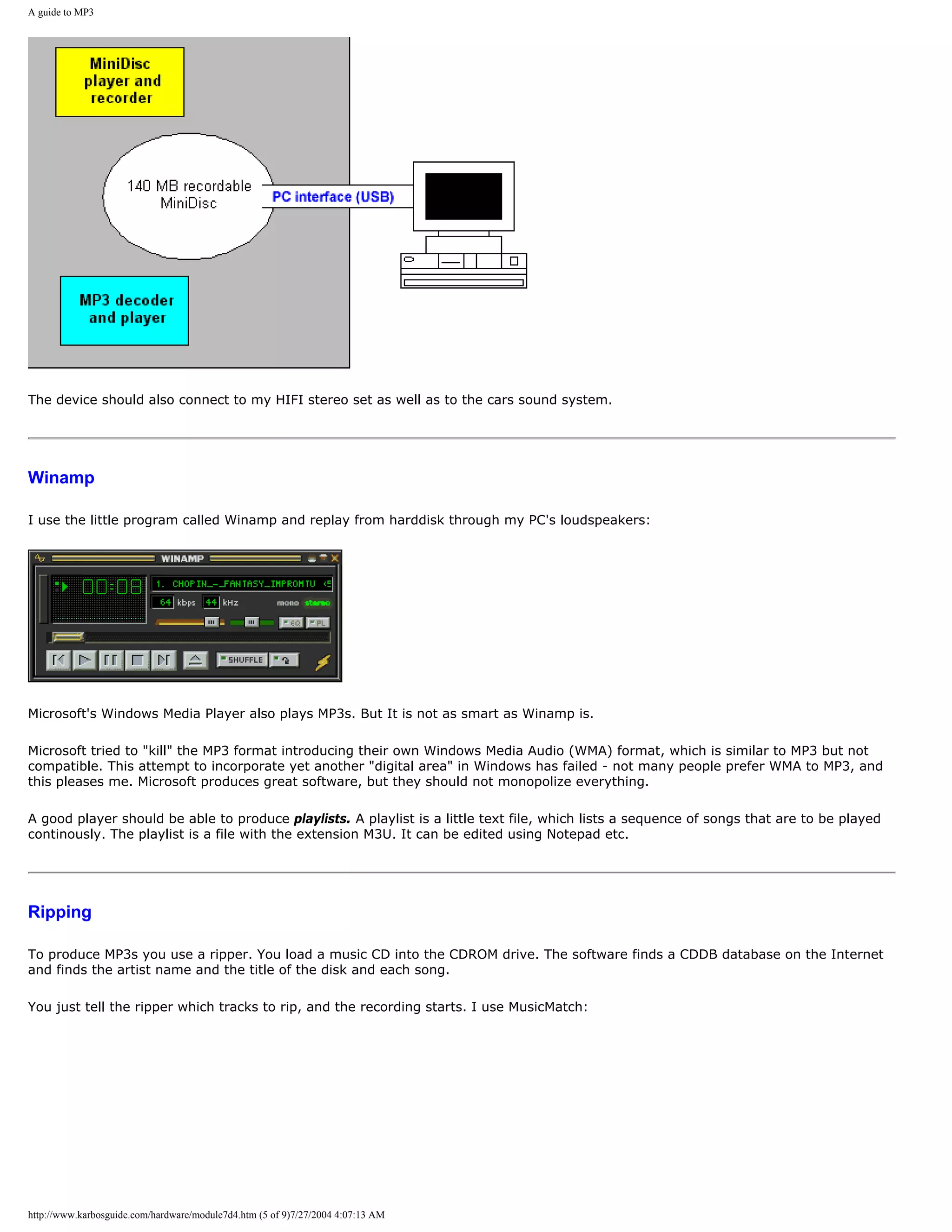
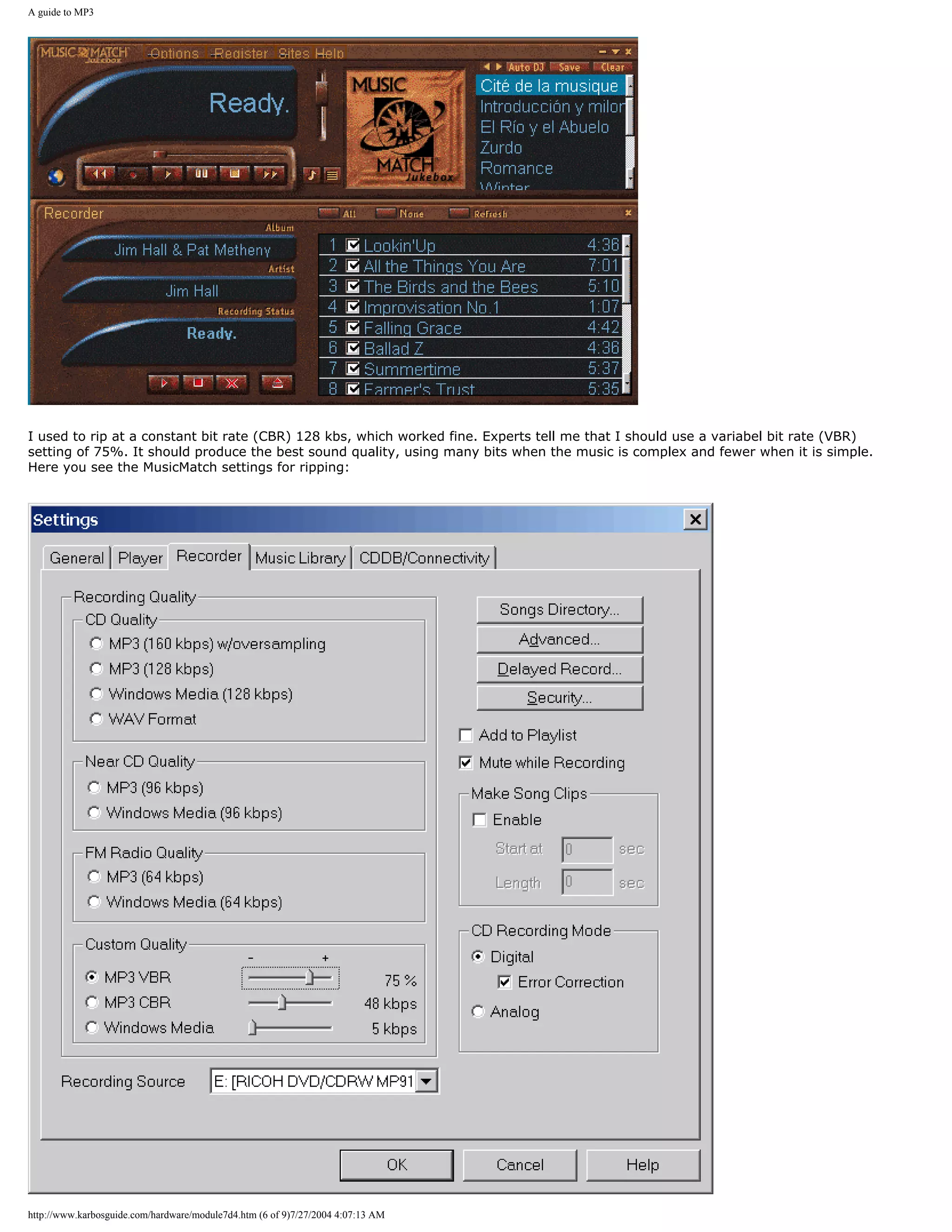
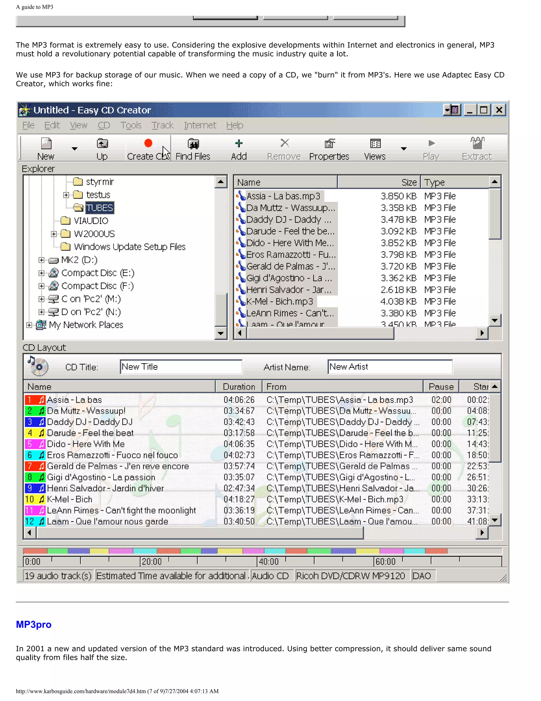
![A guide to MP3
Here you see my DVD-player which plays CD-ROMs filled with MP3 files:
Links
[top]
Get a MP3 player
You will have to find the MP3s yourself - start with www.mp3.com
Get a ripper from MusicMatch
Microsoft's new player " Windows Media Player " also plays MP3s.
q Next page
q Previous page
Learn more [top]
Click for Module 3b about CPU improvements
Click for Module 3c about the 5th generations CPUs (Pentiums etc.)
Click for Module 3d about the clock frequencies
Click for Module 3e about 6th generations CPUs (Pentium IIs etc.)
http://www.karbosguide.com/hardware/module7d4.htm (8 of 9)7/27/2004 4:07:13 AM](https://image.slidesharecdn.com/computerhardware-michaelkarbo-121118154249-phpapp01/75/Computer-hardware-michael-karbo-216-2048.jpg)
![A guide to MP3
[Main page] [Contact] [Karbo's Dictionary] [The Software Guides]
Copyright (c) 1996-2001 by Michael B. Karbo. www.karbosguide.com.
http://www.karbosguide.com/hardware/module7d4.htm (9 of 9)7/27/2004 4:07:13 AM](https://image.slidesharecdn.com/computerhardware-michaelkarbo-121118154249-phpapp01/75/Computer-hardware-michael-karbo-217-2048.jpg)
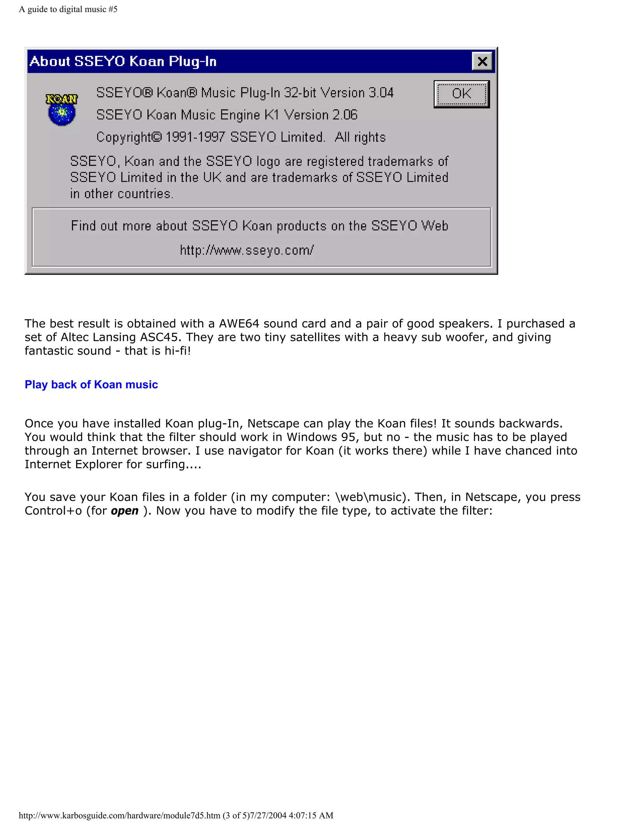
![A guide to digital music #5
Now you just select the melody, and Netscape will play it. You need not be on the Internet, you
just use the browser to play the music. The music can run in the background all day, while you
do something else.
If the SKP files are associated with Netscape, you can play them directly by double clicking on
them.
Links
[top]
At the SSEYO Koan home page you can find plugins, tunes and information, including software to
let you write your own Koan music.
q Next page
http://www.karbosguide.com/hardware/module7d5.htm (4 of 5)7/27/2004 4:07:15 AM](https://image.slidesharecdn.com/computerhardware-michaelkarbo-121118154249-phpapp01/75/Computer-hardware-michael-karbo-221-2048.jpg)
![A guide to digital music #5
q Previous page
Learn more [top]
Click for Module 3b about CPU improvements
Click for Module 3c about the 5th generations CPUs (Pentiums etc.)
Click for Module 3d about the clock frequencies
Click for Module 3e about 6th generations CPUs (Pentium IIs etc.)
[Main page] [Contact] [Karbo's Dictionary] [The Software Guides]
Copyright (c) 1996-2001 by Michael B. Karbo. www.karbosguide.com.
http://www.karbosguide.com/hardware/module7d5.htm (5 of 5)7/27/2004 4:07:15 AM](https://image.slidesharecdn.com/computerhardware-michaelkarbo-121118154249-phpapp01/75/Computer-hardware-michael-karbo-222-2048.jpg)