
Download to read offline
![International Journal of Engineering Inventions
ISSN: 2278-7461, www.ijeijournal.com
Volume 1, Issue 8 (October2012) PP: 14-19
A ROBUST PERFORMANCE OF A VOLTAGE SOURCE
CONVERTER BASED HIGH VOLTAGE DIRECT CURRENT
Nadir Ghanemi 1, Djamel Labed2,
1 ,2
Electrical Laboratory of Constantine, Constantine University, Algeria
Abstract:––In this paper, we presented the modelling of VSC (Voltage Source Converter) of a DC link in the field of Park.
A control strategy based on the separation of active and reactive power is proposed. Simulation in Matlab / Simulink system
proposed under normal operation and faulty operation allows us to evaluate the performance of a VSC HVDC.
Keywords:––VSC, HVDC, decoupled control
I. INTRODUCTION
The power transmission DC has being historically the first used solution, but the technology of that time did not
allow the development of this type of power transmission.
The first power transmission system using HVDC (High Voltage Direct Current) was released in 1954 [1], since then
research on power transmission DC has started.
Nowadays, and following the progress of the field of power electronics, converters based on VSC technology are realized
with IGBT (Insulated Gate Bipolar Transistor). These showed many advantages [1], [2] as compared to converters used for
the traditional HVDC and are realised with thyristors.
In this study, we present a model of the VSC HVDC that will allow us to establish a mathematical model, or a so called
control strategy. This model for separating control is used to power the controlled converter VSC. A simulation with
Matlab / simulink is performed to highlight the performance of a VSC HVDC.
II. MODELING OF THE VSC HVDC
The configuration of a single polar VSC [1] is given by "Fig. 1".
Rated AC voltages can be expressed by the following formula:
diabc
Vcabc V xabc L rI abc (1)
dt
Our goal is to establish a mathematical model that will be used for the control law. For this, we choose the study in the area
of Park, or we will establish a control system called VSC control by powers decoupled.
Fig. 1 VSC HVDC single polar
To facilitate the calculation, we used the transformation of Clark. This transformation the following result:
abc dq
The transition from normal reference to real reference Clark is given by "(2)":
1 1
1
2 2 a
2 3 3
0 . b
2
(2)
0 3 2
1 1 1 c
2
2 2
Transformation using the Clark "(1)":
ISSN: 2278-7461 www.ijeijournal.com P a g e | 14](https://image.slidesharecdn.com/c0181419-121124023031-phpapp02/75/C0181419International-Journal-of-Engineering-Inventions-IJEI-1-2048.jpg)
![A ROBUST PERFORMANCE OF A VOLTAGE
di
Vc Vx L rI (3)
dt
The relation between the Park reference and the Clark reference is given by:
X X dq .e jwt (4)
Where is the angular velocity of Park reference as compared to the real reference.
Using the formula "(3)," and "(4)":
d (idq .e jwt )
Vcdqe jwt V xdqe jwt L rI dq e jwt (5)
dt
On the other hand, we have:
d ( I dq .e jwt ) d ( I dq .) d (.e jwt )
L L.e jwt . L.I dq . (6)
dt dt dt
d ( I dq .e jwt ) d ( I dq .)
L L.e jwt . jwL.I dq .e jwt (7)
dt dt
If we substitute "(7)," in "(5),", and eliminate the term e jwt :
dI dq
Vcdq Vxdq L jwLI dq rI dq (8)
dt
The equation "(8)," represents the mathematical model of a Single Polar VSC configuration in the Park reference.
III. CONTROL OF THE VSC HVDC
If we consider the axis ( d ) of reference ( dq ) is in phase with the voltage (A) of the real reference, this means
that for every moment Vxd Vx [3], [4]. Therefore, the equation "(8)," becomes:
dI d
Vcd V xd L dt jwLI d rI d
(9)
V 0 L dI q jwLI rI
cq
dt
q q
With:
jI d I q And jI q I d (10)
Applying the Laplace transform on the results "(9)," and "(10),"
( SL r ) I d Vcd V xd wLI q
SL r I q Vcq wLI d
(11)
1. Inner current controllers
The principle of inner control is based on current formula "(11)". This type of control allows through a reference
currents ( I d ) and ( I q ) of the generated reference voltage ( V d ) and ( V q ) for generating control pulses for VSC converters.
The block diagram of the inner control current is given by "Fig. 2".
Fig. 2 Inner current controllers
ISSN: 2278-7461 www.ijeijournal.com P a g e | 15](https://image.slidesharecdn.com/c0181419-121124023031-phpapp02/75/C0181419International-Journal-of-Engineering-Inventions-IJEI-2-2048.jpg)
![A ROBUST PERFORMANCE OF A VOLTAGE
2. Outer controllers
The power exchanged with the alternative network through the VSC in the Park reference is given by the formula
"(12)," [5]:
S
3
2
V xd jV xq . I d jI q (12)
With Vxq 0 , the equation "(12)," becomes:
3 3
S V xd .I d j V xd .I q (13)
2 2
Hence the active and reactive powers are:
3
P 2 V xd .I d
(14)
Q 3 V .I
2
xd q
On the other hand, the variation of the DC voltage can be expressed as follows [3]:
qcap 1
C
VDC icap dt (15)
C
With ( C ) represent the smoothing capacitor voltage DC side.
If we neglect the power losses in converters (rectifier, inverter), and apply the theorem of energy conservation, we can write:
3
V xd I d V DC icap V DC I DC 0 (16)
2
From "(15)," and "(16)," we have:
dV DC 3V xd 2V I
I d DC DC (17)
dt 2CV DC 3V xd
From equation "(14)," controlled VSC in active and reactive powers can be formed separately. For the control voltage and
according to the equation "(17)", the DC voltage is affected by the current ( I d ) and ( V xd ).
If we consider an AC electrical network low-power SCR 2 (Short Circuit Ratio) the ( V xd ) has a value almost constant,
this means that the voltage ( V DC ) is dependant on only the current ( I d ).
The control structure is given by "Fig. 3"
Fig. 3 Outer controllers
Generally, the converters using a technique VSC are controlled [6] [7] by active and reactive powers for the
rectifier mode, reactive power and DC voltage for inverter mode.
The complete structure of the VSC control is given by "Fig. 4".
ISSN: 2278-7461 www.ijeijournal.com P a g e | 16](https://image.slidesharecdn.com/c0181419-121124023031-phpapp02/75/C0181419International-Journal-of-Engineering-Inventions-IJEI-3-2048.jpg)
![A ROBUST PERFORMANCE OF A VOLTAGE
Fig. 4 VSC HVDC controllers
The controllers PI (Proportional Integrator) of the control system are calculated using the symmetrical optimum
criterion [2], [8], Table (1) gives the different gains of the controllers.
Table I. GAINS OF THE CONTROLLERS
Outre controllers Inner controllers
PI
KP KI KP KI
P (station1) 0,17 12 7 85
Q (station1) 0,12 12 3 55
V (station2) 1 26 5 45
Q (station2) 0,3 25 3 35
IV. SIMULATION AND RESULTS
To test the performance of the VSC HVDC transmission under normal operation (change of control settings), and
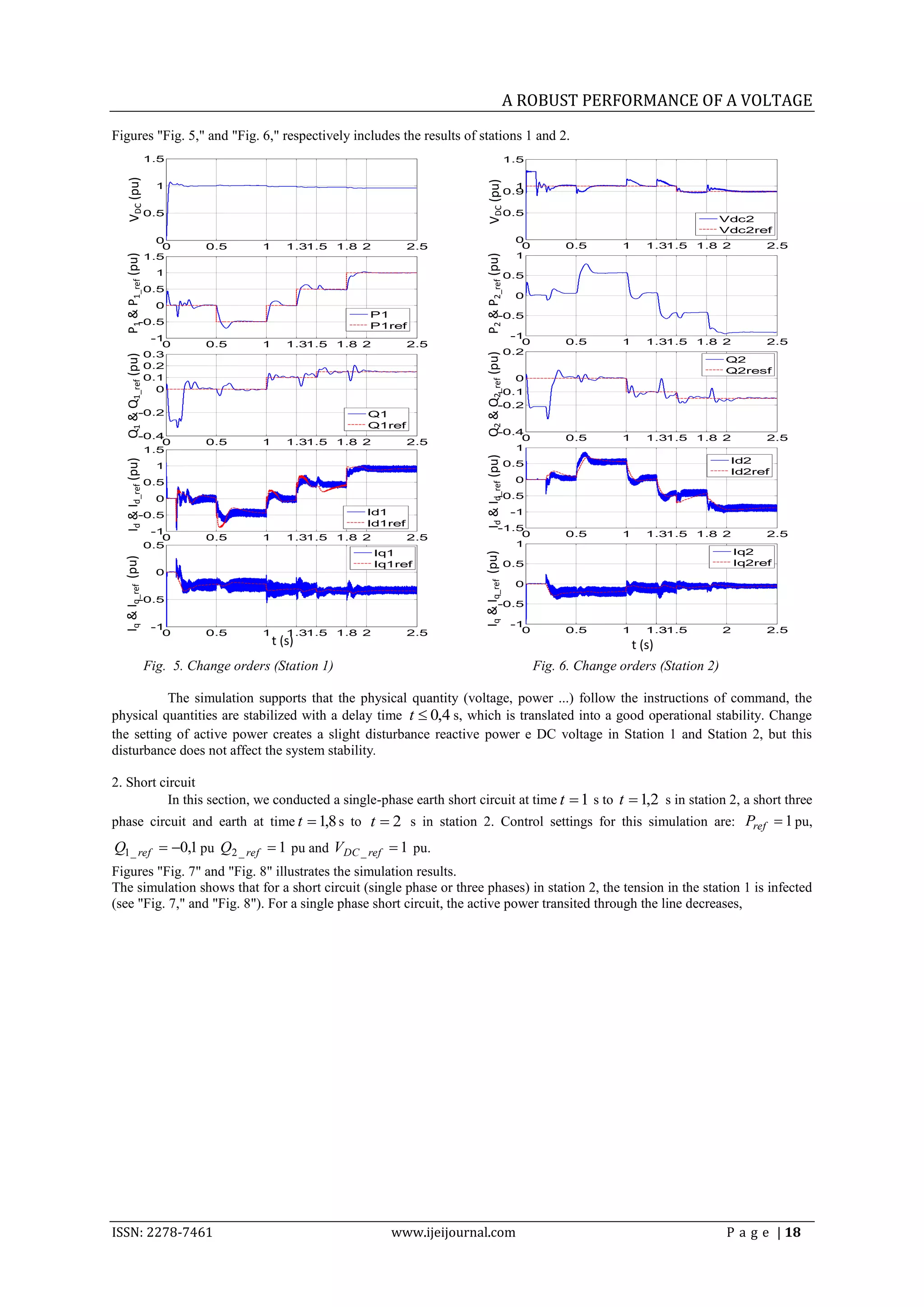
a default operation (single and three phase short circuit) was selected see the network "Fig. 5".
Fig. 5 Testing network
1. Variations in the command instructions
In the first simulation, we will test the response of the VSC-HVDC for changes in control settings.
Initial settings : Pref 0 pu, Q1 _ ref 0 pu, Q2 _ ref 0 pu et VDC _ ref 1 pu.
The scenario change is given in Table II.
Table II. VARIATION OF THE SETTINGS
time (s) Pref Q1 _ ref Q2 _ ref VDC _ ref
0,5 -0,5 0 0 1
1 0 0,1 -0,1 1
1,3 0 0,1 -0,1 1
1,5 0,5 0,15 -0,15 0,9
1,8 1 0,15 -0,15 0,9
ISSN: 2278-7461 www.ijeijournal.com P a g e | 17](https://image.slidesharecdn.com/c0181419-121124023031-phpapp02/75/C0181419International-Journal-of-Engineering-Inventions-IJEI-4-2048.jpg)
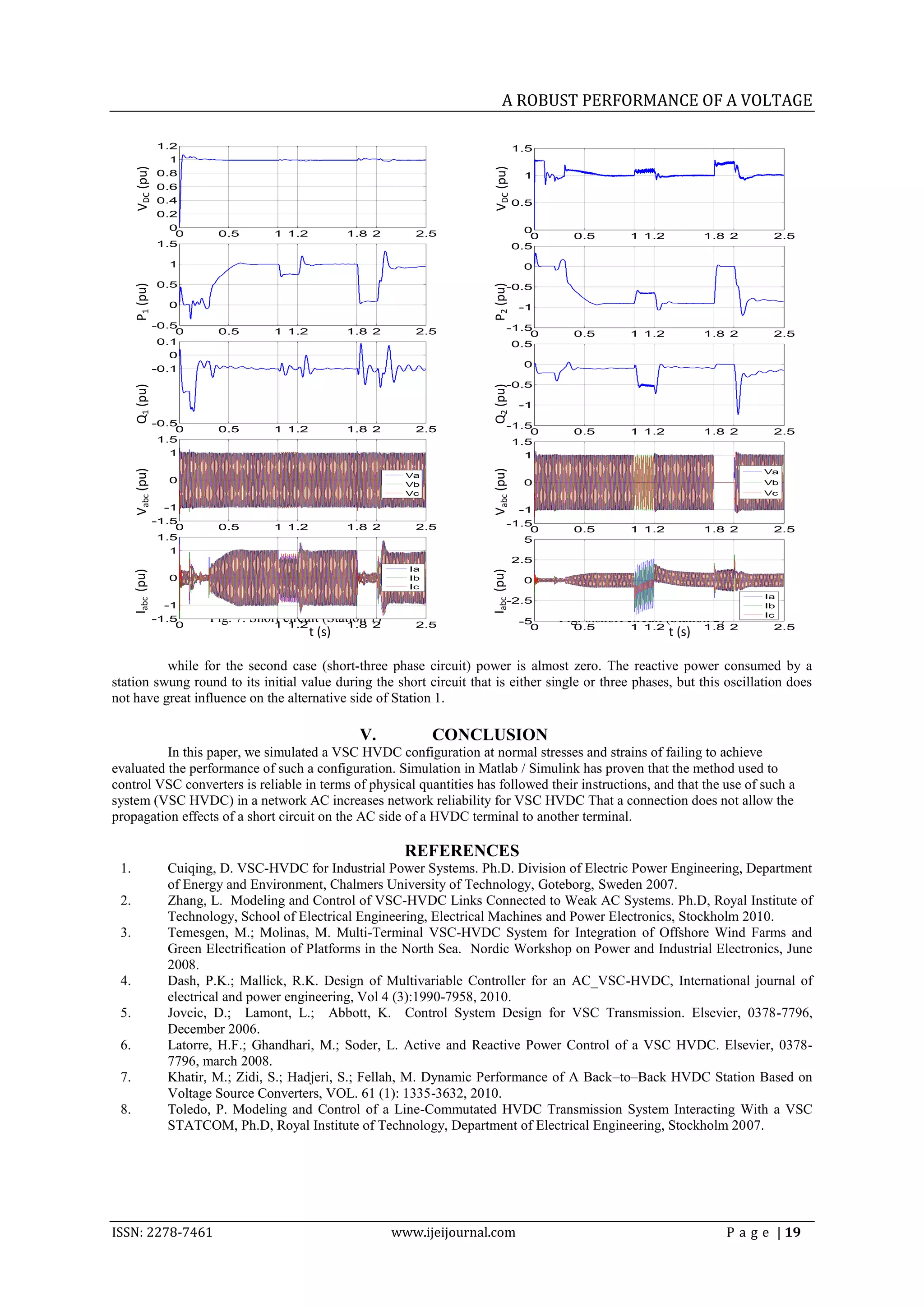
This document summarizes a research paper that models and simulates the control of a voltage source converter (VSC) for high voltage direct current (HVDC) power transmission. The summary is: 1) A mathematical model of a VSC HVDC system is developed using Park's transformation to facilitate control system design. 2) An inner current control loop and outer power/voltage control loops are proposed based on decoupled control of active and reactive power. 3) Simulations under normal and faulty operations demonstrate the control system provides robust performance for the VSC HVDC with disturbances rejecting in less than 0.4 seconds.


![Empc 8-110329 a[1]](https://cdn.slidesharecdn.com/ss_thumbnails/empc-8-110329a1-110905021306-phpapp01-thumbnail.jpg?width=640&height=640&fit=bounds)


