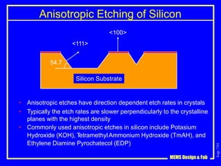
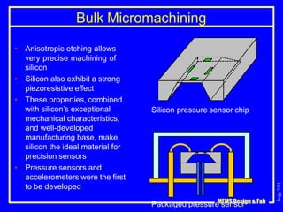
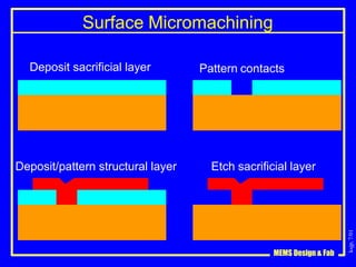
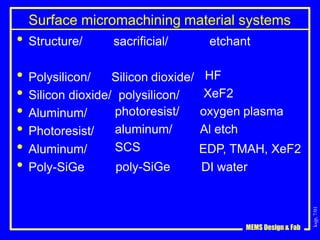
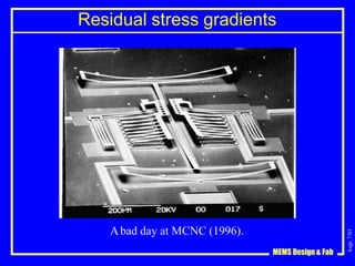
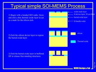
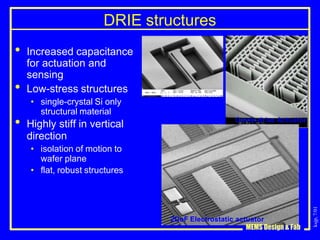
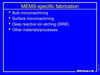
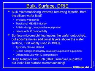
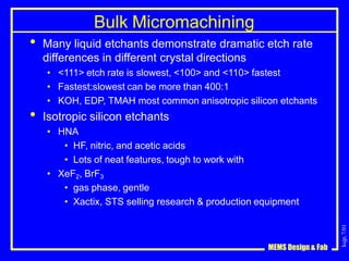
This document discusses different microelectromechanical systems (MEMS) fabrication techniques including bulk micromachining, surface micromachining, and deep reactive ion etching (DRIE). Bulk micromachining involves removing material from the silicon wafer through wet etching, typically using anisotropic etchants like potassium hydroxide (KOH) or tetramethylammonium hydroxide (TMAH) that etch at different rates depending on the crystal orientation. Surface micromachining leaves the wafer intact but adds and removes additional layers on the surface, first used widely in the 1990s. DRIE removes substrate in a way that looks like surface micromachining.

![ksjp,
7/01
Crystal Planes & Miller Indices
• [abc] in a cubic crystal is just a direction vector
• (abc) is any plane perpendicular to the [abc] vector
• (…)/[…] indicate a specific plane/direction
• {…}/<…> indicate equivalent planes/direction
Angles between directions can be determined by scalar
product: the angle between [abc] and [xyz] is given by
ax+by+cz = |(a,b,c)|*|(x,y,z)|*cos(theta)
e.g.: ((1 0 0) /(1)( 3))
MEMS Design & Fab
1
(100),(111) Cos](https://image.slidesharecdn.com/bulksurfacemicromachining-240228161853-0789d87b/85/bulk-surface-micromachining-and-engg-stuff-about-mems-5-320.jpg)
![ksjp,
7/01
Miller indices
[100]
[010]
[001]
b
c
a
[abc]
MEMS Design & Fab](https://image.slidesharecdn.com/bulksurfacemicromachining-240228161853-0789d87b/85/bulk-surface-micromachining-and-engg-stuff-about-mems-6-320.jpg)
![ksjp,
7/01
MEMS Design & Fab
[010]
[001]
a
b
c
[abc]
1/a
[100]
1/b
1/c
(abc)](https://image.slidesharecdn.com/bulksurfacemicromachining-240228161853-0789d87b/85/bulk-surface-micromachining-and-engg-stuff-about-mems-7-320.jpg)
![ksjp,
7/01
MEMS Design & Fab
[100]
[001]
(100)
{100}
(001)
[010]
(010)](https://image.slidesharecdn.com/bulksurfacemicromachining-240228161853-0789d87b/85/bulk-surface-micromachining-and-engg-stuff-about-mems-8-320.jpg)
![ksjp,
7/01
MEMS Design & Fab
[100]
[001]
(110)
[010]
(111)](https://image.slidesharecdn.com/bulksurfacemicromachining-240228161853-0789d87b/85/bulk-surface-micromachining-and-engg-stuff-about-mems-9-320.jpg)
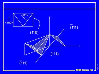
![ksjp,
7/01
MEMS Design & Fab
Typical 100 wafer
Cross-section in (110) plane
<111>
<100>
The wafer flat is oriented in the [110] direction](https://image.slidesharecdn.com/bulksurfacemicromachining-240228161853-0789d87b/85/bulk-surface-micromachining-and-engg-stuff-about-mems-10-320.jpg)