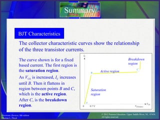
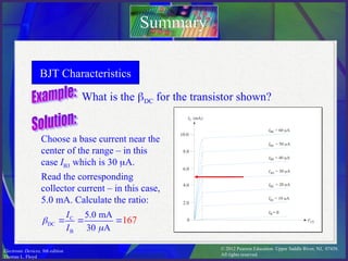
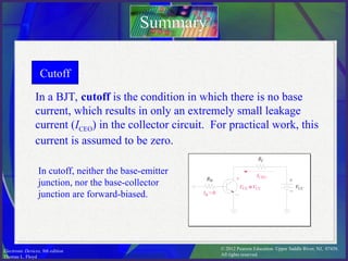
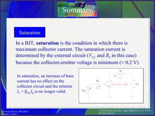
© 2012 Pearson Education. Upper Saddle River, NJ, 07458.
All rights reserved.
Electronic Devices, 9th edition
Thomas L. Floyd
Electronic Devices
Ninth Edition
Floyd
Chapter 4
© 2012 Pearson Education. Upper Saddle River, NJ, 07458.
All rights reserved.
Electronic Devices, 9th edition
Thomas L. Floyd
BJT Structure
The BJT has three regions called the emitter, base, and
collector. Between the regions are junctions as indicated.
Summary
Summary
B
(base)
C(collector)
n
p
n
Base-Collector
junction
Base-Emitter
junction
E (emitter)
B
C
p
n
E
p
npn pnp
The base is a thin
lightly doped region
compared to the
heavily doped emitter
and moderately doped
collector regions.
© 2012 Pearson Education. Upper Saddle River, NJ, 07458.
All rights reserved.
Electronic Devices, 9th edition
Thomas L. Floyd
BJT Operation
In normal operation, the base-emitter is forward-biased
and the base-collector is reverse-biased.
Summary
Summary
npn
For the pnp type, the voltages
are reversed to maintain the
forward-reverse bias.
–
+ –
+
–
+
+
BCreverse-
biased
–
BE forward-
biased
–
+
+
–
–
BCreverse-
biased
+
BE forward-
biased
–
+
pnp
For the npn type shown, the
collector is more positive
than the base, which is more
positive than the emitter.
© 2012 Pearson Education. Upper Saddle River, NJ, 07458.
All rights reserved.
Electronic Devices, 9th edition
Thomas L. Floyd
BJT Currents
Summary
Summary
IE IE
IC
IB
IC
IB
n
p
n
p
n
p
+
– +
–
–
+
IE
IC
IB
+
–
+
IE
IC
IB
+
–
–
npn pnp
The direction of conventional current is in the direction of the arrow
on the emitter terminal. The emitter current is the sum of the
collector current and the small base current. That is, IE = IC + IB.
© 2012 Pearson Education. Upper Saddle River, NJ, 07458.
All rights reserved.
Electronic Devices, 9th edition
Thomas L. Floyd
Summary
Summary
The collector characteristic curves show the relationship
of the three transistor currents.
The curve shown is for a fixed
based current. The first region is
the saturation region.
BJT Characteristics
IC
B
C
A
0 0.7 V VCE(max)
VCE
Saturation
region
Active region
Breakdown
region
As VCE is increased, IC increases
until B. Then it flattens in
region between points B and C,
which is the active region.
After C, is the breakdown
region.
© 2012 Pearson Education. Upper Saddle River, NJ, 07458.
All rights reserved.
Electronic Devices, 9th edition
Thomas L. Floyd
Summary
Summary
The collector characteristic curves illustrate the relationship of the
three transistor currents.
0
IC
VCE
IB6
IB5
IB4
IB3
IB2
IB1
IB = 0
Cutoff region
By setting up other values of
base current, a family of
collector curves is developed.
DC is the ratio of collector
current to base current.
BJT Characteristics
It can be read from the curves.
The value of DC is nearly the
same wherever it is read.
C
DC
B
I
I
 
© 2012 Pearson Education. Upper Saddle River, NJ, 07458.
All rights reserved.
Electronic Devices, 9th edition
Thomas L. Floyd
Summary
Summary
What is the DC for the transistor shown?
Choose a base current near the
center of the range – in this
case IB3 which is 30 A.
IC
VCE
IB6
IB5
IB4
B3
I
IB2
B1
I
IB = 0
= 10 A
m
= 20 A
m
= 30 A
m
= 0
= 60 A
m
= 40 A
m
= 50 A
m
10.0
8.0
6.0
4.0
2.0
0
(mA)
Read the corresponding
collector current – in this case,
5.0 mA. Calculate the ratio:
C
DC
B
5.0 mA
30 A
I
I


  167
BJT Characteristics
© 2012 Pearson Education. Upper Saddle River, NJ, 07458.
All rights reserved.
Electronic Devices, 9th edition
Thomas L. Floyd
Cutoff
Summary
Summary
In a BJT, cutoff is the condition in which there is no base
current, which results in only an extremely small leakage
current (ICEO) in the collector circuit. For practical work, this
current is assumed to be zero.
IB =0 –
+
–
+
ICEO
RC
VCC
VCE ≅VCC
RB
In cutoff, neither the base-emitter
junction, nor the base-collector
junction are forward-biased.
© 2012 Pearson Education. Upper Saddle River, NJ, 07458.
All rights reserved.
Electronic Devices, 9th edition
Thomas L. Floyd
Saturation
Summary
Summary
In a BJT, saturation is the condition in which there is
maximum collector current. The saturation current is
determined by the external circuit (VCC and RC in this case)
because the collector-emitter voltage is minimum (≈ 0.2 V)
In saturation, an increase of base
current has no effect on the
collector circuit and the relation
IC = DCIB is no longer valid. –
+ –
+
VCC
VBB
VCE = VCC – IC RC
RB
RC
IB
IC
–
+
– +
© 2012 Pearson Education. Upper Saddle River, NJ, 07458.
All rights reserved.
Electronic Devices, 9th edition
Thomas L. Floyd
DC Load Line
Summary
Summary
the transistor. It is drawn by
connecting the saturation
and cutoff points.
The transistor characteristic
curves are shown
superimposed on the load line.
The region between the
saturation and cutoff points is
called the active region.
The DC load line represents the circuit that is external to
0
IC
VCE
IB =0 Cutoff
VCE(sat) VCC
IC(sat)
Saturation
© 2012 Pearson Education. Upper Saddle River, NJ, 07458.
All rights reserved.
Electronic Devices, 9th edition
Thomas L. Floyd
DC Load Line
Summary
Summary
What is the saturation current and
the cutoff voltage for the circuit?
Assume VCE = 0.2 V in saturation. –
+ –
+
VCC
15 V
VBB
3 V
RC
RB
βDC =200
220 kW
3.3 kW
CC
SAT
C
0.2 V 15 V 0.2 V
3.3 k
V
I
R
 
  

4.48 mA CO CC
V V
 15 V
Is the transistor saturated? B
3.0 V 0.7 V
10.45 A
220 k
I 

 

IC =  IB = 200 (10.45 A) = 2.09 mA Since IC < ISAT, it is not saturated.
© 2012 Pearson Education. Upper Saddle River, NJ, 07458.
All rights reserved.
Electronic Devices, 9th edition
Thomas L. Floyd
Data Sheets
Summary
Summary
Data sheets give manufacturer’s specifications for maximum operating
conditions, thermal, and electrical characteristics. For example, an
electrical characteristic is DC, which is given as hFE. The 2N3904 shows
a range of ’s on the data sheet from 100 to 300 for IC = 10 mA.
ON Characteristics
DC current gain
(IC = 0.1 mA dc, VCE = 1.0 Vdc)
(IC = 1.0 mA dc, VCE = 1.0 Vdc)
(IC = 10 mA dc, VCE = 1.0 V dc)
(IC = 50 mA dc, VCE = 1.0 V dc)
(IC = 100 mA dc, VCE = 1.0 V dc)
2N3903
2N3904
2N3903
2N3904
2N3903
2N3904
2N3903
2N3904
2N3903
2N3904
hFE
20
40
35
70
50
100
30
60
15
30
–
–
–
–
150
300
–
–
–
–
–
Characteristic Symbol Max Unit
Min
© 2012 Pearson Education. Upper Saddle River, NJ, 07458.
All rights reserved.
Electronic Devices, 9th edition
Thomas L. Floyd
DC and AC Quantities
Summary
Summary
The text uses capital letters for both AC and DC currents and voltages
with rms values assumed unless stated otherwise.
DC Quantities use upper case roman subscripts. Example: VCE.
(The second letter in the subscript indicates the reference point.)
AC Quantities and time varying signals use lower case italic
subscripts. Example: Vce.
Internal transistor resistances are indicated as lower case
quantities with a prime and an appropriate subscript. Example: re
’
.
External resistances are indicated as capital R with either a
capital or lower case subscript depending on if it is a DC or ac
resistance. Examples: RC and Rc.
© 2012 Pearson Education. Upper Saddle River, NJ, 07458.
All rights reserved.
Electronic Devices, 9th edition
Thomas L. Floyd
BJT Amplifiers
Summary
Summary
A BJT amplifies AC signals by converting some of the DC power from
the power supplies to AC signal power. An ac signal at the input is
superimposed in the dc bias by the capacitive coupling. The output ac
signal is inverted and rides on a dc level of VCE.
–
+
–
+
VCC
VBB
RB
RC
Vb
Vc
r′
e
Vin
VCE
Vc
VBB
Vin
0
0
© 2012 Pearson Education. Upper Saddle River, NJ, 07458.
All rights reserved.
Electronic Devices, 9th edition
Thomas L. Floyd
BJT Switches
Summary
Summary
A BJT can be used as a switching device in logic circuits to turn on or
off current to a load. As a switch, the transistor is normally in either
cutoff (load is OFF) or saturation (load is ON).
In cutoff, the transistor
looks like an open switch.
In saturation, the transistor
looks like a closed switch.
RB
0 V
RC IC =0
+VCC
RC
C
E
+VCC
IB =0
–
+
RB
RC IC(sat)
+VCC
RC
C
E
+VCC
IB
+VBB
IC(sat)
© 2012 Pearson Education. Upper Saddle River, NJ, 07458.
All rights reserved.
Electronic Devices, 9th edition
Thomas L. Floyd
Phototransistors
Summary
Summary
A phototransistor produces base current when light strikes the exposed
photosensitive base region, which is the active area. Phototransistors
have high gain and are more sensitive to light than photodiodes.
Collector
Emitter
Light
n p
n
Base
In a typical circuit the base
lead is left open. In the
circuit shown, the output
voltage is maximum with
no light and drops with
increasing light.
RC
+V
VO U T
CC
© 2012 Pearson Education. Upper Saddle River, NJ, 07458.
All rights reserved.
Electronic Devices, 9th edition
Thomas L. Floyd
Phototransistors
Summary
Summary
The characteristic curves for a phototransistor are based on light flux
(mW/cm2
) to the base rather than base current in an ordinary transistor.
Dark current
5
0 10 15 20 25 30
VCE (V)
10
8
6
4
2
IC (mA)
50 mW/cm2
2
2
2
10 mW/cm2
© 2012 Pearson Education. Upper Saddle River, NJ, 07458.
All rights reserved.
Electronic Devices, 9th edition
Thomas L. Floyd
Phototransistors
Summary
Summary
The output from the phototransistor can be used to activate or deactivate
a relay. In this case, the phototransistor is part of a switching circuit.
+VCC
R
Relay
coil
Relay
contacts
Q2
Q1
Is either transistor ON for the circuit
when there is no incident light?
With no incident light, Q1 will be
biased OFF. Q2 will be forward-biased
through R and is ON. Collector current
in Q2 causes the relay to be energized.
© 2012 Pearson Education. Upper Saddle River, NJ, 07458.
All rights reserved.
Electronic Devices, 9th edition
Thomas L. Floyd
Optocouplers
Summary
Summary
An optocoupler is a single package containing
an LED and a phototransistor. Optical couplers
transfer a signal from one circuit to another
while providing a high degree of isolation.
A key specification for optocouplers is the current transfer ratio or
CTR, which is a measure of efficiency. The CTR is the ratio of
output current to input current. Typically values are from 50% to
110% for standard optocouplers.
© 2012 Pearson Education. Upper Saddle River, NJ, 07458.
All rights reserved.
Electronic Devices, 9th edition
Thomas L. Floyd
Applications for Optocouplers
Summary
Summary
Optocouplers are used when data or signals need to be
transferred from a control circuit to a power circuit
without making electrical connections between the
circuits. For example, the logic circuits in a traffic light
controller need to be isolated from the lights themselves.
Another application for optocouplers is as a transducer to detect a
light path such as a hole in a rotating disk. In this case, the LED
and phototransistor are separated by a gap.
Optocouplers are also useful for isolating patients
from the monitoring instruments.
Traffic
Controller
© 2012 Pearson Education. Upper Saddle River, NJ, 07458.
All rights reserved.
Electronic Devices, 9th edition
Thomas L. Floyd
A Sample of Common Transistor Packages
Summary
Summary
1
2
3
1 Emitter
2
Base
3 Collector
TO-92
2 Emitter
1
Base
3 Collector
1
2
3
SOT-23
1 Emitter
2
Base
3 Collector
3 2
1
TO-18
C(case)
E
B
TO-3
B
C
E
C
TO-220AB
E
C
B
TO-225AA
© 2012 Pearson Education. Upper Saddle River, NJ, 07458.
All rights reserved.
Electronic Devices, 9th edition
Thomas L. Floyd
BJT Basic Test
A basic test for a BJT is to use the Diode Test function of your DMM.
VW
1 s
1 s
40 mA
10 A
COM
Range
Autorange
Touch/Hold
Fused
OFF V
V
mV
Hz
W
A
H
H
H
0.673 V
E B C
Summary
Summary
VW
1 s
1 s
40 mA
10 A
COM
Range
Autorange
Touch/Hold
Fused
OFF V
V
mV
Hz
W
A
H
H
H
OL
E B C
To test the base-emitter junction of a
BJT, connect the positive lead to the
base and the negative lead to the
emitter. You should see a voltage
close to 0.7 V for an npn transistor.
Reversing the leads will show OL
for “overload”.
The procedure is repeated to test the
base-collector junction.
© 2012 Pearson Education. Upper Saddle River, NJ, 07458.
All rights reserved.
Electronic Devices, 9th edition
Thomas L. Floyd
Selected Key Terms
Selected Key Terms
BJT (bipolar
junction
transistor)
Emitter
Base
Collector
a transistor constructed with three doped
semiconductor regions separated by two pn
junctions.
the most heavily doped of the three
semiconductor regions of a BJT.
one of the three semiconductor regions of a BJT.
The base is thin and lightly doped compared to
the other regions.
the largest of the three semiconductor regions of
a BJT.
© 2012 Pearson Education. Upper Saddle River, NJ, 07458.
All rights reserved.
Electronic Devices, 9th edition
Thomas L. Floyd
Selected Key Terms
Selected Key Terms
Beta
Saturation
Cutoff
Phototransistor
the ratio of dc collector current to the dc base
current in a BJT; current gain from base to
collector.
the state of a BJT in which the collector
current has reached a maximum and is
independent of the base current.
the nonconducting state of a transistor.
a transistor in which base current is produced
when like strikes the photosensitive
semiconductor base region.
© 2012 Pearson Education. Upper Saddle River, NJ, 07458.
All rights reserved.
Electronic Devices, 9th edition
Thomas L. Floyd
Quiz
Quiz
1. The region on the characteristic curve in which the
current changes only slightly with an increase in VCE is
called the
a. saturation region
b. cutoff region
c. breakdown region
d. active region
© 2012 Pearson Education. Upper Saddle River, NJ, 07458.
All rights reserved.
Electronic Devices, 9th edition
Thomas L. Floyd
Quiz
Quiz
2. DC is defined as the ratio of
a. collector current to base current
b. collector current to emitter current
c. emitter current to base current
d. emitter current to collector current
© 2012 Pearson Education. Upper Saddle River, NJ, 07458.
All rights reserved.
Electronic Devices, 9th edition
Thomas L. Floyd
Quiz
Quiz
a. collector current does not change with an
increase in base current
b. base current cannot increase
c. collector to emitter voltage is maximum
d. all of the above
3. When a BJT is in saturation, the
© 2012 Pearson Education. Upper Saddle River, NJ, 07458.
All rights reserved.
Electronic Devices, 9th edition
Thomas L. Floyd
Quiz
Quiz
4. When a BJT is cutoff, the
a. voltage from collector to emitter is near zero
b. collector current is near zero
c. base-emitter junction is forward-biased
d. none of the above
© 2012 Pearson Education. Upper Saddle River, NJ, 07458.
All rights reserved.
Electronic Devices, 9th edition
Thomas L. Floyd
Quiz
Quiz
5. The lower end of the dc load line touches the x-axis at
a. saturation
b. cutoff
c. breakdown
d. 0.7 V
© 2012 Pearson Education. Upper Saddle River, NJ, 07458.
All rights reserved.
Electronic Devices, 9th edition
Thomas L. Floyd
Quiz
Quiz
6. For the circuit shown, the base current is
a. 1.0 A
b. 1.16 A
c. 10 A
d. 11.6 A –
+ –
+
VCC
15 V
VBB
5 V
RC
RB
βDC =200
430 kW
3.9 kW
© 2012 Pearson Education. Upper Saddle River, NJ, 07458.
All rights reserved.
Electronic Devices, 9th edition
Thomas L. Floyd
Quiz
Quiz
7. For the circuit shown, the saturation current is
a. 200 A
b. 2.0 mA
c. 3.79 mA
d. 14.8 mA –
+ –
+
VCC
15 V
VBB
5 V
RC
RB
βDC =200
430 kW
3.9 kW
© 2012 Pearson Education. Upper Saddle River, NJ, 07458.
All rights reserved.
Electronic Devices, 9th edition
Thomas L. Floyd
Quiz
Quiz
8. For the phototransistor circuit, assume there is sufficient
light to saturate Q1. In this condition,
a. Q2 is also saturated
b. the diode is conducting
c. the relay is energized
d. none of the above
+VCC
R
Relay
coil
Relay
contacts
Q2
Q1
© 2012 Pearson Education. Upper Saddle River, NJ, 07458.
All rights reserved.
Electronic Devices, 9th edition
Thomas L. Floyd
Quiz
Quiz
9. An optocoupler is a single package containing
a. two transistors
b. an LED and a phototransistor
c. a phototransistor and a relay
d. an LED and a relay
© 2012 Pearson Education. Upper Saddle River, NJ, 07458.
All rights reserved.
Electronic Devices, 9th edition
Thomas L. Floyd
Quiz
Quiz
10. The transistor package that is a TO-3 case is
a. b.
c. d.
© 2012 Pearson Education. Upper Saddle River, NJ, 07458.
All rights reserved.
Electronic Devices, 9th edition
Thomas L. Floyd
Quiz
Quiz
Answers:
1. d
2. a
3. a
4. d
5. b
6. c
7. c
8. d
9. b
10. c

Basic Electronics Lecture Electronic Devices Chapter 4

  • 1.
    © 2012 PearsonEducation. Upper Saddle River, NJ, 07458. All rights reserved. Electronic Devices, 9th edition Thomas L. Floyd Electronic Devices Ninth Edition Floyd Chapter 4
  • 2.
    © 2012 PearsonEducation. Upper Saddle River, NJ, 07458. All rights reserved. Electronic Devices, 9th edition Thomas L. Floyd BJT Structure The BJT has three regions called the emitter, base, and collector. Between the regions are junctions as indicated. Summary Summary B (base) C(collector) n p n Base-Collector junction Base-Emitter junction E (emitter) B C p n E p npn pnp The base is a thin lightly doped region compared to the heavily doped emitter and moderately doped collector regions.
  • 3.
    © 2012 PearsonEducation. Upper Saddle River, NJ, 07458. All rights reserved. Electronic Devices, 9th edition Thomas L. Floyd BJT Operation In normal operation, the base-emitter is forward-biased and the base-collector is reverse-biased. Summary Summary npn For the pnp type, the voltages are reversed to maintain the forward-reverse bias. – + – + – + + BCreverse- biased – BE forward- biased – + + – – BCreverse- biased + BE forward- biased – + pnp For the npn type shown, the collector is more positive than the base, which is more positive than the emitter.
  • 4.
    © 2012 PearsonEducation. Upper Saddle River, NJ, 07458. All rights reserved. Electronic Devices, 9th edition Thomas L. Floyd BJT Currents Summary Summary IE IE IC IB IC IB n p n p n p + – + – – + IE IC IB + – + IE IC IB + – – npn pnp The direction of conventional current is in the direction of the arrow on the emitter terminal. The emitter current is the sum of the collector current and the small base current. That is, IE = IC + IB.
  • 5.
    © 2012 PearsonEducation. Upper Saddle River, NJ, 07458. All rights reserved. Electronic Devices, 9th edition Thomas L. Floyd Summary Summary The collector characteristic curves show the relationship of the three transistor currents. The curve shown is for a fixed based current. The first region is the saturation region. BJT Characteristics IC B C A 0 0.7 V VCE(max) VCE Saturation region Active region Breakdown region As VCE is increased, IC increases until B. Then it flattens in region between points B and C, which is the active region. After C, is the breakdown region.
  • 6.
    © 2012 PearsonEducation. Upper Saddle River, NJ, 07458. All rights reserved. Electronic Devices, 9th edition Thomas L. Floyd Summary Summary The collector characteristic curves illustrate the relationship of the three transistor currents. 0 IC VCE IB6 IB5 IB4 IB3 IB2 IB1 IB = 0 Cutoff region By setting up other values of base current, a family of collector curves is developed. DC is the ratio of collector current to base current. BJT Characteristics It can be read from the curves. The value of DC is nearly the same wherever it is read. C DC B I I  
  • 7.
    © 2012 PearsonEducation. Upper Saddle River, NJ, 07458. All rights reserved. Electronic Devices, 9th edition Thomas L. Floyd Summary Summary What is the DC for the transistor shown? Choose a base current near the center of the range – in this case IB3 which is 30 A. IC VCE IB6 IB5 IB4 B3 I IB2 B1 I IB = 0 = 10 A m = 20 A m = 30 A m = 0 = 60 A m = 40 A m = 50 A m 10.0 8.0 6.0 4.0 2.0 0 (mA) Read the corresponding collector current – in this case, 5.0 mA. Calculate the ratio: C DC B 5.0 mA 30 A I I     167 BJT Characteristics
  • 8.
    © 2012 PearsonEducation. Upper Saddle River, NJ, 07458. All rights reserved. Electronic Devices, 9th edition Thomas L. Floyd Cutoff Summary Summary In a BJT, cutoff is the condition in which there is no base current, which results in only an extremely small leakage current (ICEO) in the collector circuit. For practical work, this current is assumed to be zero. IB =0 – + – + ICEO RC VCC VCE ≅VCC RB In cutoff, neither the base-emitter junction, nor the base-collector junction are forward-biased.
  • 9.
    © 2012 PearsonEducation. Upper Saddle River, NJ, 07458. All rights reserved. Electronic Devices, 9th edition Thomas L. Floyd Saturation Summary Summary In a BJT, saturation is the condition in which there is maximum collector current. The saturation current is determined by the external circuit (VCC and RC in this case) because the collector-emitter voltage is minimum (≈ 0.2 V) In saturation, an increase of base current has no effect on the collector circuit and the relation IC = DCIB is no longer valid. – + – + VCC VBB VCE = VCC – IC RC RB RC IB IC – + – +
  • 10.
    © 2012 PearsonEducation. Upper Saddle River, NJ, 07458. All rights reserved. Electronic Devices, 9th edition Thomas L. Floyd DC Load Line Summary Summary the transistor. It is drawn by connecting the saturation and cutoff points. The transistor characteristic curves are shown superimposed on the load line. The region between the saturation and cutoff points is called the active region. The DC load line represents the circuit that is external to 0 IC VCE IB =0 Cutoff VCE(sat) VCC IC(sat) Saturation
  • 11.
    © 2012 PearsonEducation. Upper Saddle River, NJ, 07458. All rights reserved. Electronic Devices, 9th edition Thomas L. Floyd DC Load Line Summary Summary What is the saturation current and the cutoff voltage for the circuit? Assume VCE = 0.2 V in saturation. – + – + VCC 15 V VBB 3 V RC RB βDC =200 220 kW 3.3 kW CC SAT C 0.2 V 15 V 0.2 V 3.3 k V I R       4.48 mA CO CC V V  15 V Is the transistor saturated? B 3.0 V 0.7 V 10.45 A 220 k I      IC =  IB = 200 (10.45 A) = 2.09 mA Since IC < ISAT, it is not saturated.
  • 12.
    © 2012 PearsonEducation. Upper Saddle River, NJ, 07458. All rights reserved. Electronic Devices, 9th edition Thomas L. Floyd Data Sheets Summary Summary Data sheets give manufacturer’s specifications for maximum operating conditions, thermal, and electrical characteristics. For example, an electrical characteristic is DC, which is given as hFE. The 2N3904 shows a range of ’s on the data sheet from 100 to 300 for IC = 10 mA. ON Characteristics DC current gain (IC = 0.1 mA dc, VCE = 1.0 Vdc) (IC = 1.0 mA dc, VCE = 1.0 Vdc) (IC = 10 mA dc, VCE = 1.0 V dc) (IC = 50 mA dc, VCE = 1.0 V dc) (IC = 100 mA dc, VCE = 1.0 V dc) 2N3903 2N3904 2N3903 2N3904 2N3903 2N3904 2N3903 2N3904 2N3903 2N3904 hFE 20 40 35 70 50 100 30 60 15 30 – – – – 150 300 – – – – – Characteristic Symbol Max Unit Min
  • 13.
    © 2012 PearsonEducation. Upper Saddle River, NJ, 07458. All rights reserved. Electronic Devices, 9th edition Thomas L. Floyd DC and AC Quantities Summary Summary The text uses capital letters for both AC and DC currents and voltages with rms values assumed unless stated otherwise. DC Quantities use upper case roman subscripts. Example: VCE. (The second letter in the subscript indicates the reference point.) AC Quantities and time varying signals use lower case italic subscripts. Example: Vce. Internal transistor resistances are indicated as lower case quantities with a prime and an appropriate subscript. Example: re ’ . External resistances are indicated as capital R with either a capital or lower case subscript depending on if it is a DC or ac resistance. Examples: RC and Rc.
  • 14.
    © 2012 PearsonEducation. Upper Saddle River, NJ, 07458. All rights reserved. Electronic Devices, 9th edition Thomas L. Floyd BJT Amplifiers Summary Summary A BJT amplifies AC signals by converting some of the DC power from the power supplies to AC signal power. An ac signal at the input is superimposed in the dc bias by the capacitive coupling. The output ac signal is inverted and rides on a dc level of VCE. – + – + VCC VBB RB RC Vb Vc r′ e Vin VCE Vc VBB Vin 0 0
  • 15.
    © 2012 PearsonEducation. Upper Saddle River, NJ, 07458. All rights reserved. Electronic Devices, 9th edition Thomas L. Floyd BJT Switches Summary Summary A BJT can be used as a switching device in logic circuits to turn on or off current to a load. As a switch, the transistor is normally in either cutoff (load is OFF) or saturation (load is ON). In cutoff, the transistor looks like an open switch. In saturation, the transistor looks like a closed switch. RB 0 V RC IC =0 +VCC RC C E +VCC IB =0 – + RB RC IC(sat) +VCC RC C E +VCC IB +VBB IC(sat)
  • 16.
    © 2012 PearsonEducation. Upper Saddle River, NJ, 07458. All rights reserved. Electronic Devices, 9th edition Thomas L. Floyd Phototransistors Summary Summary A phototransistor produces base current when light strikes the exposed photosensitive base region, which is the active area. Phototransistors have high gain and are more sensitive to light than photodiodes. Collector Emitter Light n p n Base In a typical circuit the base lead is left open. In the circuit shown, the output voltage is maximum with no light and drops with increasing light. RC +V VO U T CC
  • 17.
    © 2012 PearsonEducation. Upper Saddle River, NJ, 07458. All rights reserved. Electronic Devices, 9th edition Thomas L. Floyd Phototransistors Summary Summary The characteristic curves for a phototransistor are based on light flux (mW/cm2 ) to the base rather than base current in an ordinary transistor. Dark current 5 0 10 15 20 25 30 VCE (V) 10 8 6 4 2 IC (mA) 50 mW/cm2 2 2 2 10 mW/cm2
  • 18.
    © 2012 PearsonEducation. Upper Saddle River, NJ, 07458. All rights reserved. Electronic Devices, 9th edition Thomas L. Floyd Phototransistors Summary Summary The output from the phototransistor can be used to activate or deactivate a relay. In this case, the phototransistor is part of a switching circuit. +VCC R Relay coil Relay contacts Q2 Q1 Is either transistor ON for the circuit when there is no incident light? With no incident light, Q1 will be biased OFF. Q2 will be forward-biased through R and is ON. Collector current in Q2 causes the relay to be energized.
  • 19.
    © 2012 PearsonEducation. Upper Saddle River, NJ, 07458. All rights reserved. Electronic Devices, 9th edition Thomas L. Floyd Optocouplers Summary Summary An optocoupler is a single package containing an LED and a phototransistor. Optical couplers transfer a signal from one circuit to another while providing a high degree of isolation. A key specification for optocouplers is the current transfer ratio or CTR, which is a measure of efficiency. The CTR is the ratio of output current to input current. Typically values are from 50% to 110% for standard optocouplers.
  • 20.
    © 2012 PearsonEducation. Upper Saddle River, NJ, 07458. All rights reserved. Electronic Devices, 9th edition Thomas L. Floyd Applications for Optocouplers Summary Summary Optocouplers are used when data or signals need to be transferred from a control circuit to a power circuit without making electrical connections between the circuits. For example, the logic circuits in a traffic light controller need to be isolated from the lights themselves. Another application for optocouplers is as a transducer to detect a light path such as a hole in a rotating disk. In this case, the LED and phototransistor are separated by a gap. Optocouplers are also useful for isolating patients from the monitoring instruments. Traffic Controller
  • 21.
    © 2012 PearsonEducation. Upper Saddle River, NJ, 07458. All rights reserved. Electronic Devices, 9th edition Thomas L. Floyd A Sample of Common Transistor Packages Summary Summary 1 2 3 1 Emitter 2 Base 3 Collector TO-92 2 Emitter 1 Base 3 Collector 1 2 3 SOT-23 1 Emitter 2 Base 3 Collector 3 2 1 TO-18 C(case) E B TO-3 B C E C TO-220AB E C B TO-225AA
  • 22.
    © 2012 PearsonEducation. Upper Saddle River, NJ, 07458. All rights reserved. Electronic Devices, 9th edition Thomas L. Floyd BJT Basic Test A basic test for a BJT is to use the Diode Test function of your DMM. VW 1 s 1 s 40 mA 10 A COM Range Autorange Touch/Hold Fused OFF V V mV Hz W A H H H 0.673 V E B C Summary Summary VW 1 s 1 s 40 mA 10 A COM Range Autorange Touch/Hold Fused OFF V V mV Hz W A H H H OL E B C To test the base-emitter junction of a BJT, connect the positive lead to the base and the negative lead to the emitter. You should see a voltage close to 0.7 V for an npn transistor. Reversing the leads will show OL for “overload”. The procedure is repeated to test the base-collector junction.
  • 23.
    © 2012 PearsonEducation. Upper Saddle River, NJ, 07458. All rights reserved. Electronic Devices, 9th edition Thomas L. Floyd Selected Key Terms Selected Key Terms BJT (bipolar junction transistor) Emitter Base Collector a transistor constructed with three doped semiconductor regions separated by two pn junctions. the most heavily doped of the three semiconductor regions of a BJT. one of the three semiconductor regions of a BJT. The base is thin and lightly doped compared to the other regions. the largest of the three semiconductor regions of a BJT.
  • 24.
    © 2012 PearsonEducation. Upper Saddle River, NJ, 07458. All rights reserved. Electronic Devices, 9th edition Thomas L. Floyd Selected Key Terms Selected Key Terms Beta Saturation Cutoff Phototransistor the ratio of dc collector current to the dc base current in a BJT; current gain from base to collector. the state of a BJT in which the collector current has reached a maximum and is independent of the base current. the nonconducting state of a transistor. a transistor in which base current is produced when like strikes the photosensitive semiconductor base region.
  • 25.
    © 2012 PearsonEducation. Upper Saddle River, NJ, 07458. All rights reserved. Electronic Devices, 9th edition Thomas L. Floyd Quiz Quiz 1. The region on the characteristic curve in which the current changes only slightly with an increase in VCE is called the a. saturation region b. cutoff region c. breakdown region d. active region
  • 26.
    © 2012 PearsonEducation. Upper Saddle River, NJ, 07458. All rights reserved. Electronic Devices, 9th edition Thomas L. Floyd Quiz Quiz 2. DC is defined as the ratio of a. collector current to base current b. collector current to emitter current c. emitter current to base current d. emitter current to collector current
  • 27.
    © 2012 PearsonEducation. Upper Saddle River, NJ, 07458. All rights reserved. Electronic Devices, 9th edition Thomas L. Floyd Quiz Quiz a. collector current does not change with an increase in base current b. base current cannot increase c. collector to emitter voltage is maximum d. all of the above 3. When a BJT is in saturation, the
  • 28.
    © 2012 PearsonEducation. Upper Saddle River, NJ, 07458. All rights reserved. Electronic Devices, 9th edition Thomas L. Floyd Quiz Quiz 4. When a BJT is cutoff, the a. voltage from collector to emitter is near zero b. collector current is near zero c. base-emitter junction is forward-biased d. none of the above
  • 29.
    © 2012 PearsonEducation. Upper Saddle River, NJ, 07458. All rights reserved. Electronic Devices, 9th edition Thomas L. Floyd Quiz Quiz 5. The lower end of the dc load line touches the x-axis at a. saturation b. cutoff c. breakdown d. 0.7 V
  • 30.
    © 2012 PearsonEducation. Upper Saddle River, NJ, 07458. All rights reserved. Electronic Devices, 9th edition Thomas L. Floyd Quiz Quiz 6. For the circuit shown, the base current is a. 1.0 A b. 1.16 A c. 10 A d. 11.6 A – + – + VCC 15 V VBB 5 V RC RB βDC =200 430 kW 3.9 kW
  • 31.
    © 2012 PearsonEducation. Upper Saddle River, NJ, 07458. All rights reserved. Electronic Devices, 9th edition Thomas L. Floyd Quiz Quiz 7. For the circuit shown, the saturation current is a. 200 A b. 2.0 mA c. 3.79 mA d. 14.8 mA – + – + VCC 15 V VBB 5 V RC RB βDC =200 430 kW 3.9 kW
  • 32.
    © 2012 PearsonEducation. Upper Saddle River, NJ, 07458. All rights reserved. Electronic Devices, 9th edition Thomas L. Floyd Quiz Quiz 8. For the phototransistor circuit, assume there is sufficient light to saturate Q1. In this condition, a. Q2 is also saturated b. the diode is conducting c. the relay is energized d. none of the above +VCC R Relay coil Relay contacts Q2 Q1
  • 33.
    © 2012 PearsonEducation. Upper Saddle River, NJ, 07458. All rights reserved. Electronic Devices, 9th edition Thomas L. Floyd Quiz Quiz 9. An optocoupler is a single package containing a. two transistors b. an LED and a phototransistor c. a phototransistor and a relay d. an LED and a relay
  • 34.
    © 2012 PearsonEducation. Upper Saddle River, NJ, 07458. All rights reserved. Electronic Devices, 9th edition Thomas L. Floyd Quiz Quiz 10. The transistor package that is a TO-3 case is a. b. c. d.
  • 35.
    © 2012 PearsonEducation. Upper Saddle River, NJ, 07458. All rights reserved. Electronic Devices, 9th edition Thomas L. Floyd Quiz Quiz Answers: 1. d 2. a 3. a 4. d 5. b 6. c 7. c 8. d 9. b 10. c