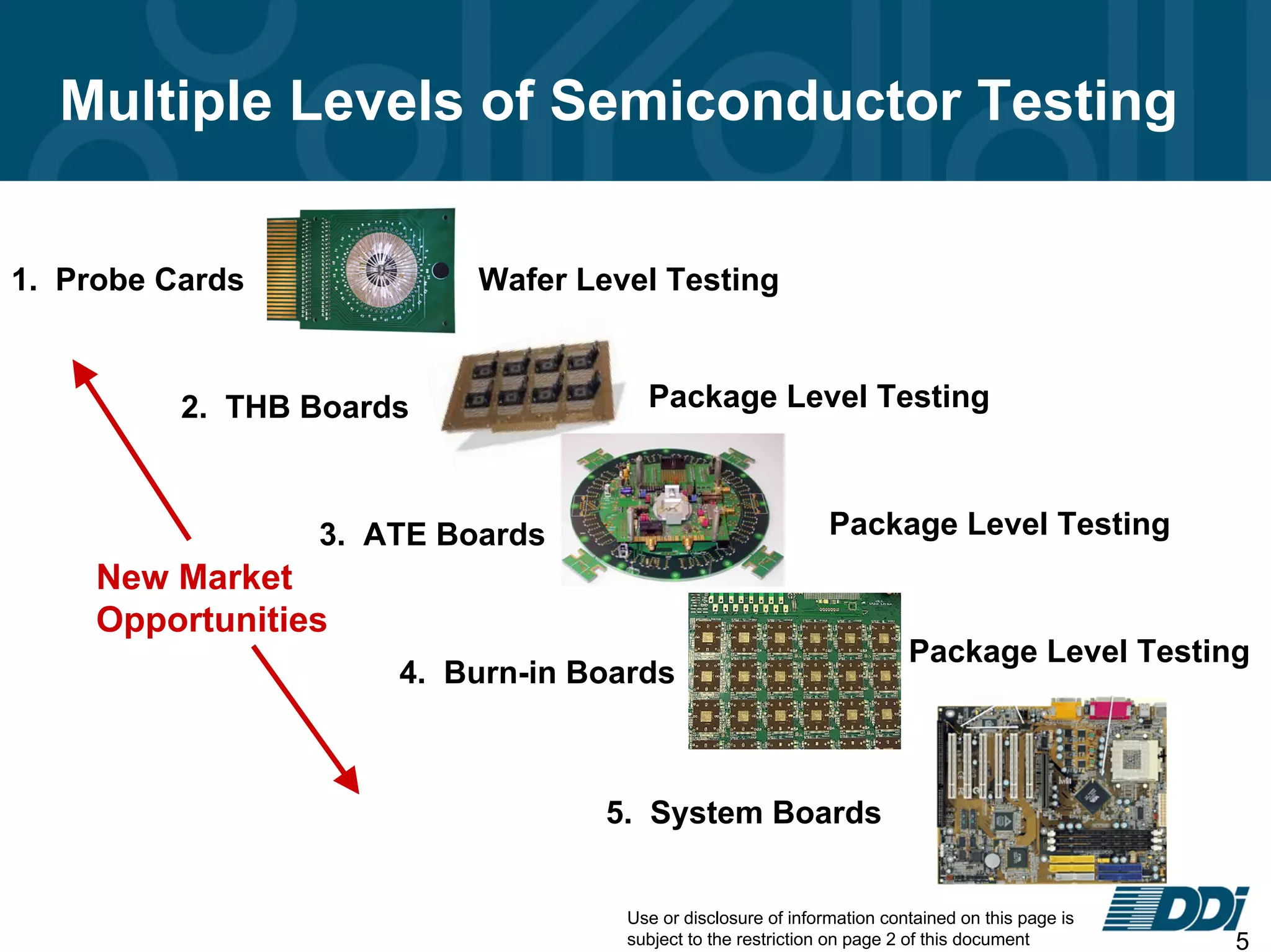
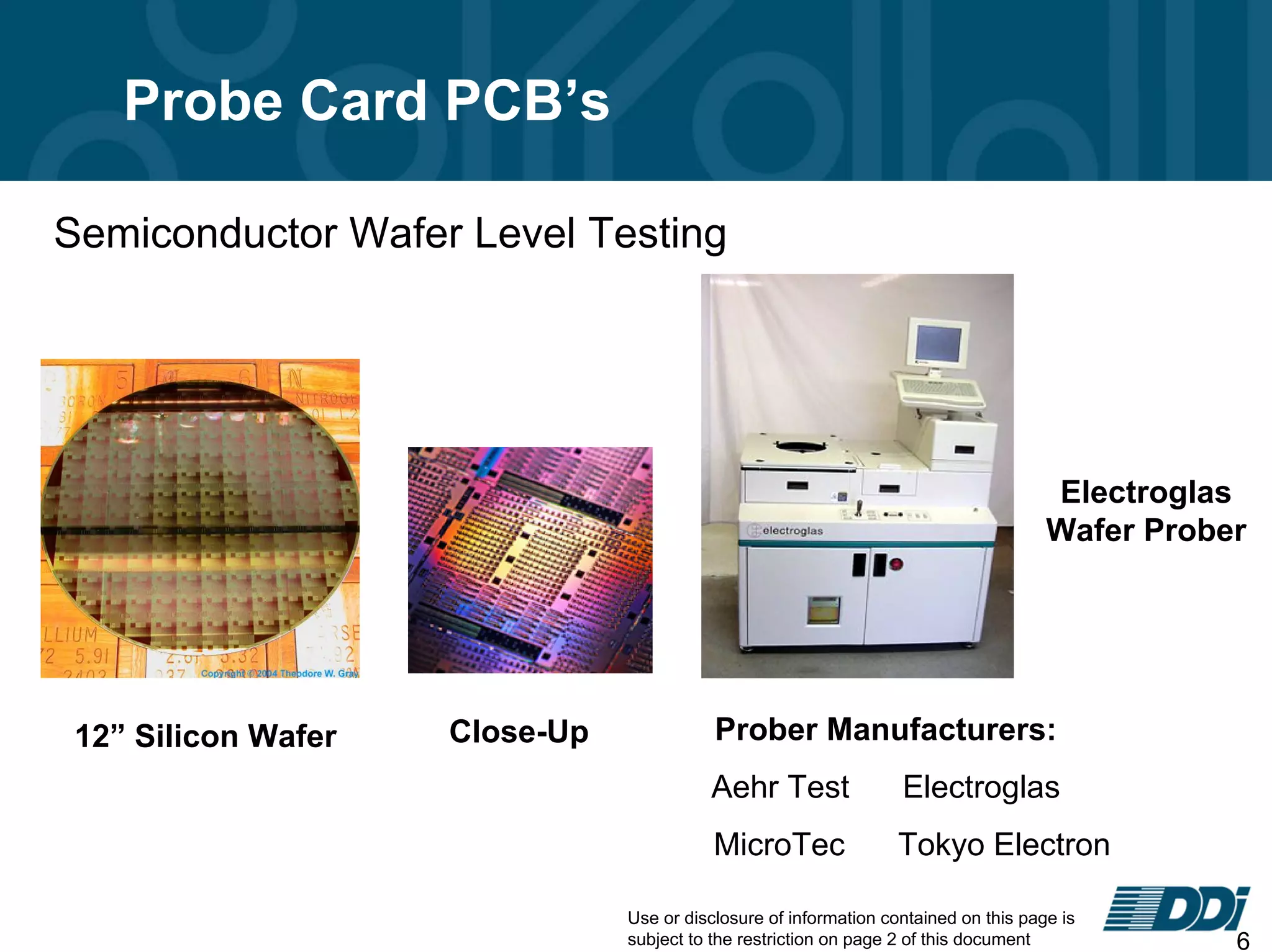
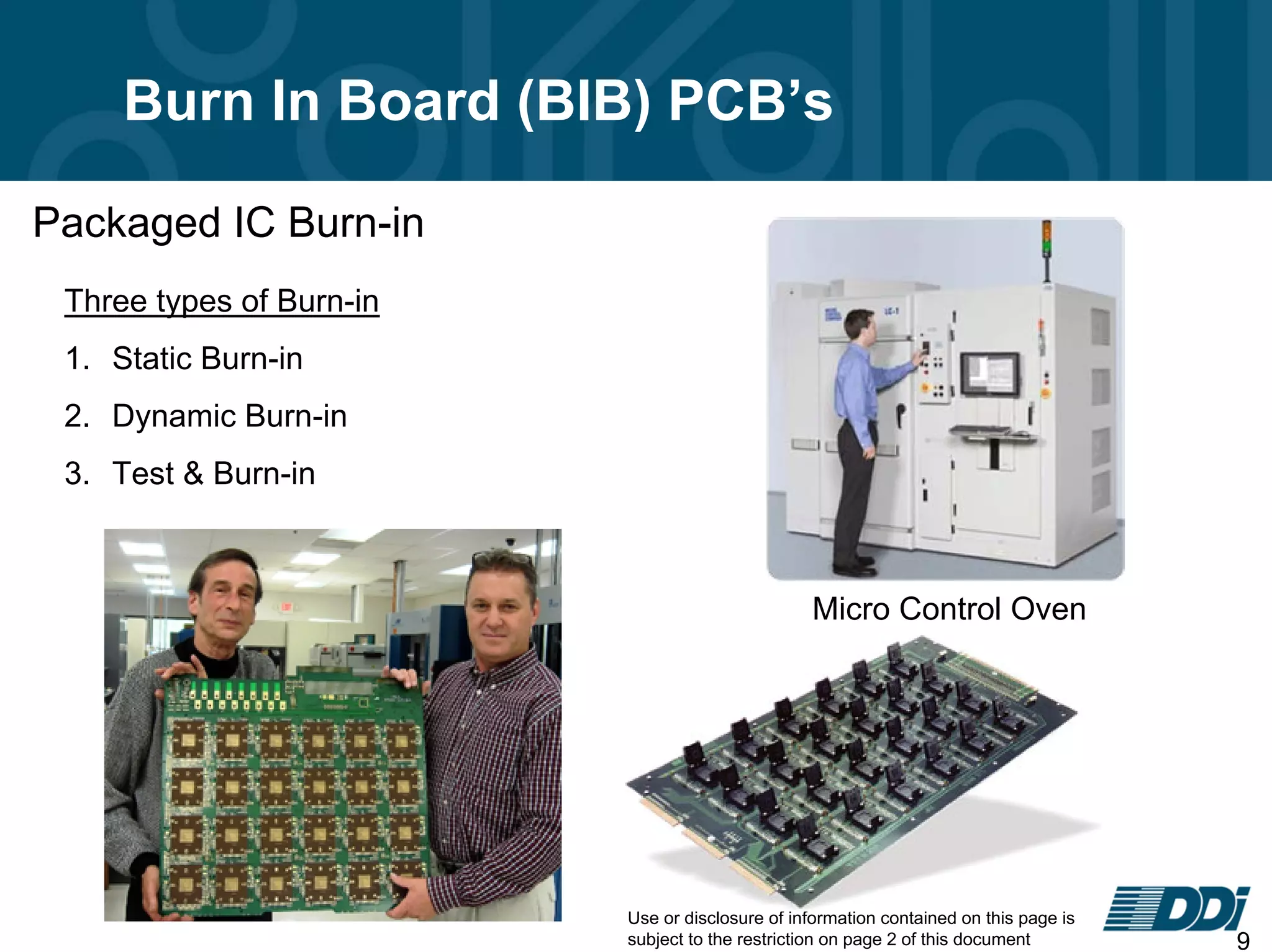
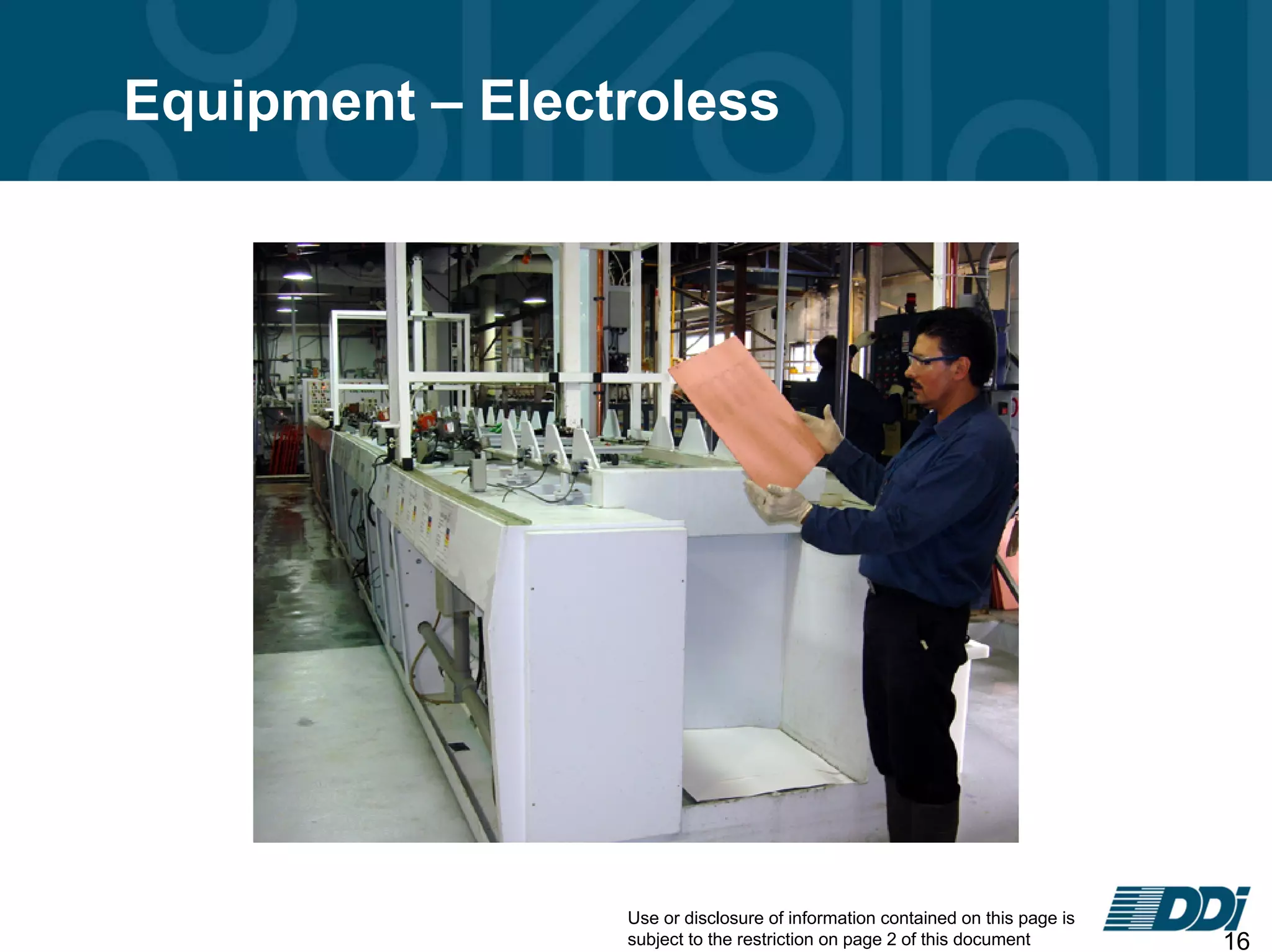
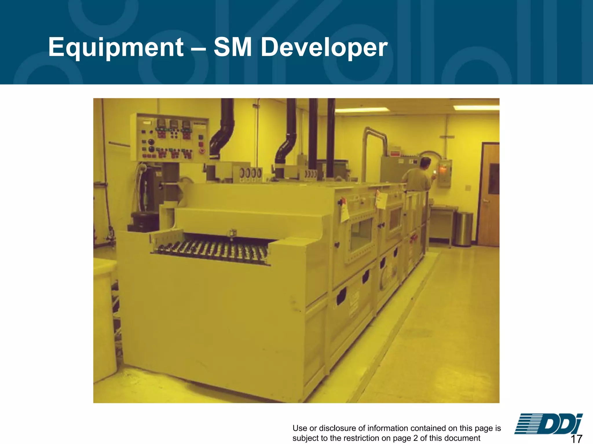
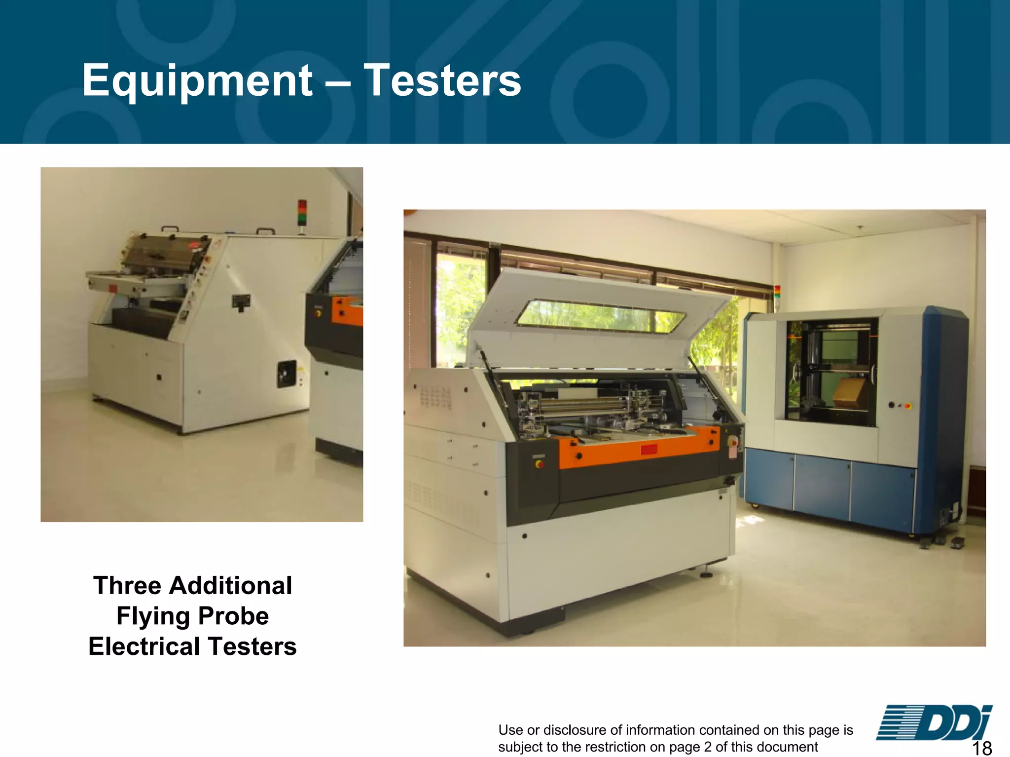
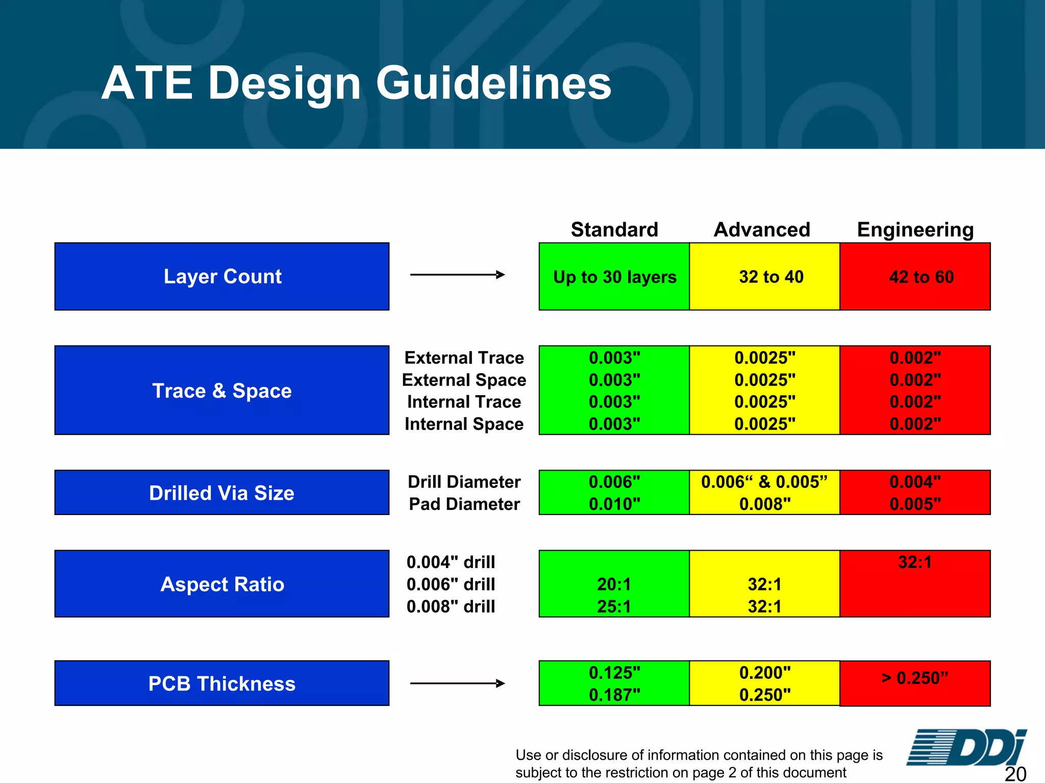
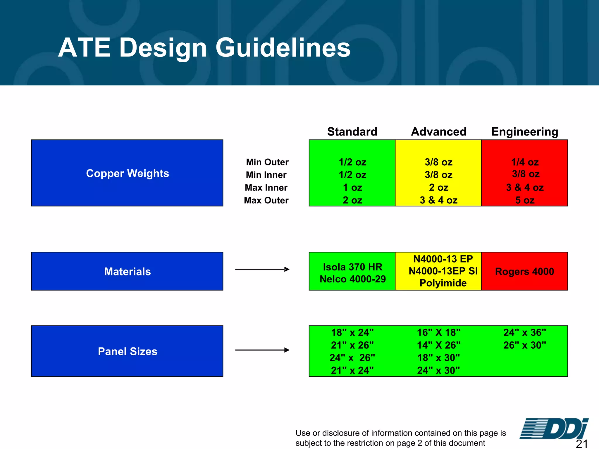
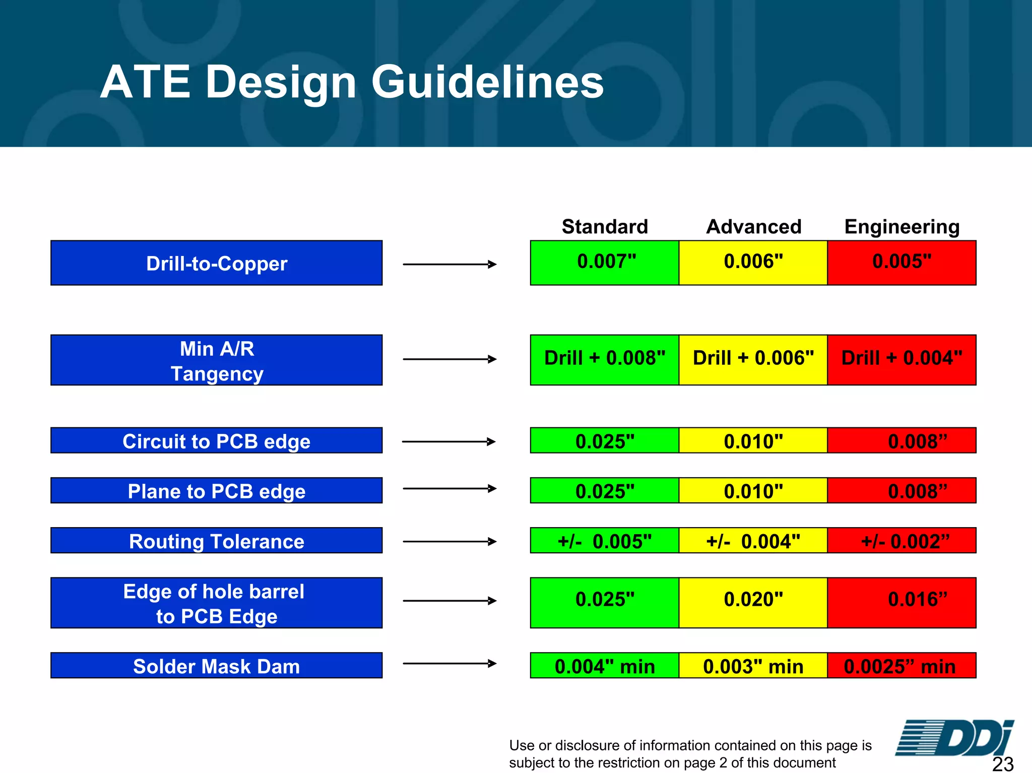
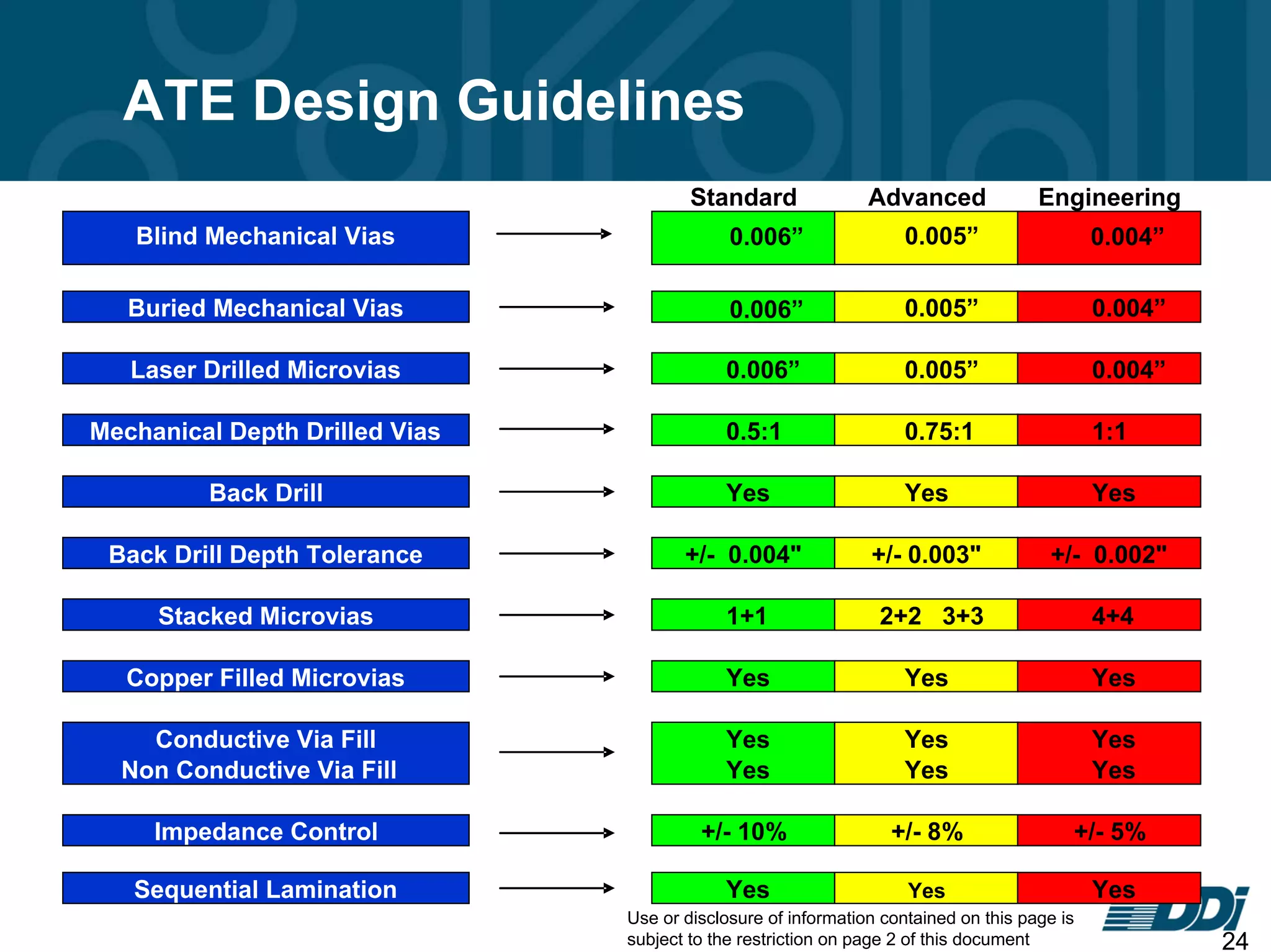
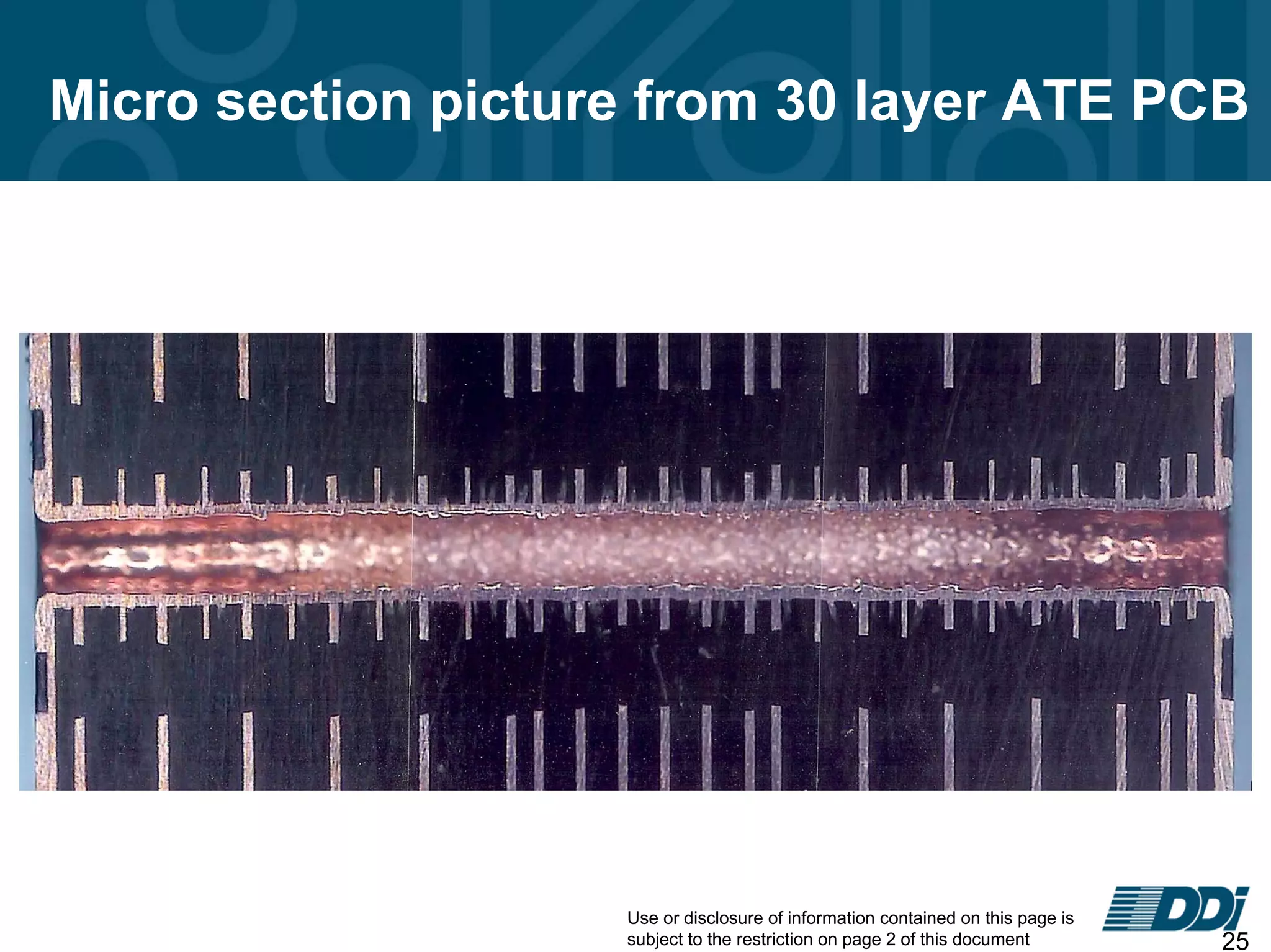
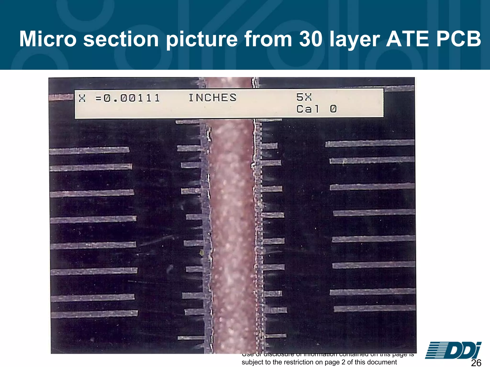
1
DDi ATE / BIB
Technology Overview
June 25, 2009
Use or disclosure of information contained on this page is
subject to the restriction on page 2 of this document 2
Notice
Notification of Proprietary Information: This document
contains proprietary information of DDi Corp. and its
receipt or possession does not convey any rights to
reproduce or disclose its contents, or to manufacture,
use, or sell anything it may describe. Reproduction,
dissemination, disclosure, or use, in whole or in part,
without specific written authorization of DDi Corp. is
strictly forbidden. All data contained within this
document are subject to this restriction.
Use or disclosure of information contained on this page is
subject to the restriction on page 2 of this document 3
ATE/BIB Market Opportunities
• DDi has been focused on the ATE and BIB market segment for some
time. We have been working with our customers to understand their
demand and technology requirements in this market sector.
• This market is important to DDi as we are always seeking to expand
our product offerings and leverage existing customer relationships
• We recently announced that we have extended our capabilities and
capacity with the acquisition of key capital and human assets to
support the high end ATE market
• This market requires specialized equipment and processing expertise
in the following areas:
– Material movement and layer to layer registration
– Lamination process controls
– High aspect ratio drilling and positional accuracy
– High aspect ratio electroless and electrolytic copper plating
– Very tight hole to copper tolerances
– Understanding of customer’s design rules and requirements
Use or disclosure of information contained on this page is
subject to the restriction on page 2 of this document 4
Semiconductor Manufacturers
Use or disclosure of information contained on this page is
subject to the restriction on page 2 of this document 5
1. Probe Cards
3. ATE Boards
2. THB Boards
5. System Boards
4. Burn-in Boards
Multiple Levels of Semiconductor Testing
Wafer Level Testing
Package Level Testing
New Market
Opportunities
Use or disclosure of information contained on this page is
subject to the restriction on page 2 of this document 6
Probe Card PCB’s
Semiconductor Wafer Level Testing
12” Silicon Wafer
Electroglas
Wafer Prober
Prober Manufacturers:
Aehr Test Electroglas
MicroTec Tokyo Electron
Close-Up
Use or disclosure of information contained on this page is
subject to the restriction on page 2 of this document 7
THB - HAST PCB’s
THB - Temperature, Humidity, Bias testing is a reliability test designed to accelerate
metal corrosion, particularly that of the metallization on the die surface of the device.
HAST - Highly Accelerated Temperature/Humidity Stress Test. It was developed as
a shorter alternative to THB testing.
Trio Tech 6000X
Pressurized Humidity Test Systems
Use or disclosure of information contained on this page is
subject to the restriction on page 2 of this document 8
ATE PCB’s
1. ATE (Automatic Test Equipment) Boards
2. DUT (Device Under Test) Boards
3. Performance Boards
4. Load Boards
Test Equipment Boards have a number of names:
Teradyne Tester
Packaged Semiconductor Testing
Use or disclosure of information contained on this page is
subject to the restriction on page 2 of this document 9
Burn In Board (BIB) PCB’s
Packaged IC Burn-in
Three types of Burn-in
1. Static Burn-in
2. Dynamic Burn-in
3. Test & Burn-in
Micro Control Oven
Use or disclosure of information contained on this page is
subject to the restriction on page 2 of this document 10
Introducing New Team Members
• John Papagni, Director ATE/BIB Technology, brings 30 years of
experience to DDi. Prior to joining DDi John was President and
CEO of Technitron, a leading producer of PCB’s for the
ATE/BIB market
• Armando Ceballos, Production Manager, will be responsible for
production training and manufacturing coordination of the
ATE/BIB product line, Armando brings 25+ years of experience
to DDi.
• Keith Lal, Senior Drill Technician, will be responsible for driving
drill technology and critical processing steps into the day to
day operations at DDi. Keith has 20+ years experience in high
aspect ratio precision drill processing of ATE/BIB PCB’s
Use or disclosure of information contained on this page is
subject to the restriction on page 2 of this document 11
DDi ATE Market Support
• Dual site approach
– Milpitas with additional equipment and engineering support
– Anaheim by leveraging current technology and expertise
– Share synergies site to site
• In Milpitas…DDi has acquired, installed, and certified the following
specialized equipment assets:
– Lamination tooling for oversized panels
– PLC controlled lamination press for tight tolerance heat rise
parameters
– High aspect ratio Electroless copper plating line
– Large Format photo printer for oversized panels
– Solder mask developer with high pressure rinse
– High speed multi-spindle drill machines for high aspect ratio
drilling
• In Anaheim…DDi has transitioned flip drill technology and high aspect
ratio pulse plating capability for this product set
Use or disclosure of information contained on this page is
subject to the restriction on page 2 of this document 12
Equipment – Lam Press
Lauffer “PLC Controlled” Hot Oil Press
Use or disclosure of information contained on this page is
subject to the restriction on page 2 of this document 13
Equipment – Pluritec & Router
Pluritec Inspecta X-Ray
Drill Position Optimizer
PDA Router
Use or disclosure of information contained on this page is
subject to the restriction on page 2 of this document 14
Equipment – Hitachi Drill Machines
Five Additional Hitachi’s
(Eight Total)
Use or disclosure of information contained on this page is
subject to the restriction on page 2 of this document 15
Equipment – Exposure & Planarizer
Large Format photo printer
MASS Planarizer
Use or disclosure of information contained on this page is
subject to the restriction on page 2 of this document 16
Equipment – Electroless
Use or disclosure of information contained on this page is
subject to the restriction on page 2 of this document 17
Equipment – SM Developer
Use or disclosure of information contained on this page is
subject to the restriction on page 2 of this document 18
Equipment – Testers
Three Additional
Flying Probe
Electrical Testers
Use or disclosure of information contained on this page is
subject to the restriction on page 2 of this document 19
• ‘DDi Standard'
DDi’s current everyday capability with no premium.
•• ‘‘DDi Advanced'DDi Advanced' = DDi’s current everyday capability
with a small premium
• ‘DDi Engineering' = product DDi has experience with
and can build on request with a significant premium
ATE Design Guidelines
Use or disclosure of information contained on this page is
subject to the restriction on page 2 of this document 20
ATE Design Guidelines
> 0.250”
Standard Advanced Engineering
Layer Count Up to 30 layers 32 to 40 42 to 60
External Trace 0.003" 0.0025" 0.002"
External Space 0.003" 0.0025" 0.002"
Internal Trace 0.003" 0.0025" 0.002"
Internal Space 0.003" 0.0025" 0.002"
Drill Diameter 0.006" 0.006“ & 0.005” 0.004"
Pad Diameter 0.010" 0.008" 0.005"
0.004" drill 32:1
0.006" drill 20:1 32:1
0.008" drill 25:1 32:1
0.125" 0.200"
0.187" 0.250"
Trace & Space
PCB Thickness
Drilled Via Size
Aspect Ratio
Use or disclosure of information contained on this page is
subject to the restriction on page 2 of this document 21
ATE Design Guidelines
Standard Advanced Engineering
Min Outer 1/2 oz 3/8 oz 1/4 oz
Min Inner 1/2 oz 3/8 oz
Max Inner 1 oz 2 oz 3 & 4 oz
Max Outer 2 oz 3 & 4 oz 5 oz
Isola 370 HR
Nelco 4000-29
N4000-13 EP
N4000-13EP SI
Polyimide
Rogers 4000
18" x 24" 16" X 18" 24" x 36"
21" x 26" 14" X 26" 26" x 30"
24" x 26" 18" x 30"
21" x 24" 24" x 30"
Materials
Panel Sizes
Copper Weights 3/8 oz
Use or disclosure of information contained on this page is
subject to the restriction on page 2 of this document 22
ATE Design Guidelines
Standard Advanced Engineering
BC2000™
FaradFlex™
Dupont HK04
Ceramic Filled
Electrolytic Gold, OSP
Lead Free HASL, ENIG
Immersion Silver, Immersion Tin
E-Less Gold
ENEPIG
Multiple
Finishes
+/- 0.0025" +/- 0.001"
0.008" 0.005"
Via Fill/Cap Plate
Non-CVF = Non-Conductive Via Fill 0.008" 0.006" 0.004"
CVF = Conductive Via Fill Non-CVF & CVF Non-CVF & CVF Non-CVF
Surface Finishes
Solder Mask Clearance
Solder Mask Opening
Embedded Passives
+/- 0.0020"
0.006"
Use or disclosure of information contained on this page is
subject to the restriction on page 2 of this document 23
ATE Design Guidelines
Standard Advanced Engineering
0.007" 0.006" 0.005"
Min A/R Drill + 0.008" Drill + 0.006" Drill + 0.004"
Tangency
Circuit to PCB edge 0.025" 0.010" 0.008”
Plane to PCB edge 0.025" 0.010" 0.008”
Routing Tolerance +/- 0.005" +/- 0.004" +/- 0.002”
Edge of hole barrel 0.025" 0.020" 0.016”
to PCB Edge
Solder Mask Dam 0.004" min 0.003" min 0.0025” min
Drill-to-Copper
Use or disclosure of information contained on this page is
subject to the restriction on page 2 of this document 24
ATE Design Guidelines
Standard Advanced Engineering
0.005”
Buried Mechanical Vias 0.005” 0.004”
Laser Drilled Microvias 0.006” 0.005” 0.004”
Mechanical Depth Drilled Vias 0.5:1 0.75:1 1:1
Back Drill Yes Yes Yes
Back Drill Depth Tolerance +/- 0.004" +/- 0.003" +/- 0.002"
Stacked Microvias 1+1 2+2 3+3 4+4
Copper Filled Microvias Yes Yes Yes
Conductive Via Fill Yes Yes Yes
Non Conductive Via Fill Yes Yes Yes
Impedance Control +/- 10% +/- 8% +/- 5%
Sequential Lamination Yes Yes Yes
Blind Mechanical Vias 0.004”0.006”
0.006”
Use or disclosure of information contained on this page is
subject to the restriction on page 2 of this document 25
Micro section picture from 30 layer ATE PCB
Use or disclosure of information contained on this page is
subject to the restriction on page 2 of this document 26
Micro section picture from 30 layer ATE PCB
Use or disclosure of information contained on this page is
subject to the restriction on page 2 of this document 27
In Summary
• The ATE/BIB market segment has been on our radar for some
time as it extends our level of support to our existing customer
base
• Recent activities have allowed us to support the high end of the
ATE technology spectrum
• Dual site approach minimizes the risk to customer and allows
for site to site synergies
• The acquisition of key talent and specialized equipment set has
enabled DDi to shorten the process development time to
support the high end market
• DDi is committed to supporting a broad spectrum of PCB
products used by a multitude of customers and this product set
will expand our offering in both regards

Ate Overview 06 25 09 Pd

  • 1.
    1 DDi ATE /BIB Technology Overview June 25, 2009
  • 2.
    Use or disclosureof information contained on this page is subject to the restriction on page 2 of this document 2 Notice Notification of Proprietary Information: This document contains proprietary information of DDi Corp. and its receipt or possession does not convey any rights to reproduce or disclose its contents, or to manufacture, use, or sell anything it may describe. Reproduction, dissemination, disclosure, or use, in whole or in part, without specific written authorization of DDi Corp. is strictly forbidden. All data contained within this document are subject to this restriction.
  • 3.
    Use or disclosureof information contained on this page is subject to the restriction on page 2 of this document 3 ATE/BIB Market Opportunities • DDi has been focused on the ATE and BIB market segment for some time. We have been working with our customers to understand their demand and technology requirements in this market sector. • This market is important to DDi as we are always seeking to expand our product offerings and leverage existing customer relationships • We recently announced that we have extended our capabilities and capacity with the acquisition of key capital and human assets to support the high end ATE market • This market requires specialized equipment and processing expertise in the following areas: – Material movement and layer to layer registration – Lamination process controls – High aspect ratio drilling and positional accuracy – High aspect ratio electroless and electrolytic copper plating – Very tight hole to copper tolerances – Understanding of customer’s design rules and requirements
  • 4.
    Use or disclosureof information contained on this page is subject to the restriction on page 2 of this document 4 Semiconductor Manufacturers
  • 5.
    Use or disclosureof information contained on this page is subject to the restriction on page 2 of this document 5 1. Probe Cards 3. ATE Boards 2. THB Boards 5. System Boards 4. Burn-in Boards Multiple Levels of Semiconductor Testing Wafer Level Testing Package Level Testing Package Level Testing Package Level Testing New Market Opportunities
  • 6.
    Use or disclosureof information contained on this page is subject to the restriction on page 2 of this document 6 Probe Card PCB’s Semiconductor Wafer Level Testing 12” Silicon Wafer Electroglas Wafer Prober Prober Manufacturers: Aehr Test Electroglas MicroTec Tokyo Electron Close-Up
  • 7.
    Use or disclosureof information contained on this page is subject to the restriction on page 2 of this document 7 THB - HAST PCB’s THB - Temperature, Humidity, Bias testing is a reliability test designed to accelerate metal corrosion, particularly that of the metallization on the die surface of the device. HAST - Highly Accelerated Temperature/Humidity Stress Test. It was developed as a shorter alternative to THB testing. Trio Tech 6000X Pressurized Humidity Test Systems
  • 8.
    Use or disclosureof information contained on this page is subject to the restriction on page 2 of this document 8 ATE PCB’s 1. ATE (Automatic Test Equipment) Boards 2. DUT (Device Under Test) Boards 3. Performance Boards 4. Load Boards Test Equipment Boards have a number of names: Teradyne Tester Packaged Semiconductor Testing
  • 9.
    Use or disclosureof information contained on this page is subject to the restriction on page 2 of this document 9 Burn In Board (BIB) PCB’s Packaged IC Burn-in Three types of Burn-in 1. Static Burn-in 2. Dynamic Burn-in 3. Test & Burn-in Micro Control Oven
  • 10.
    Use or disclosureof information contained on this page is subject to the restriction on page 2 of this document 10 Introducing New Team Members • John Papagni, Director ATE/BIB Technology, brings 30 years of experience to DDi. Prior to joining DDi John was President and CEO of Technitron, a leading producer of PCB’s for the ATE/BIB market • Armando Ceballos, Production Manager, will be responsible for production training and manufacturing coordination of the ATE/BIB product line, Armando brings 25+ years of experience to DDi. • Keith Lal, Senior Drill Technician, will be responsible for driving drill technology and critical processing steps into the day to day operations at DDi. Keith has 20+ years experience in high aspect ratio precision drill processing of ATE/BIB PCB’s
  • 11.
    Use or disclosureof information contained on this page is subject to the restriction on page 2 of this document 11 DDi ATE Market Support • Dual site approach – Milpitas with additional equipment and engineering support – Anaheim by leveraging current technology and expertise – Share synergies site to site • In Milpitas…DDi has acquired, installed, and certified the following specialized equipment assets: – Lamination tooling for oversized panels – PLC controlled lamination press for tight tolerance heat rise parameters – High aspect ratio Electroless copper plating line – Large Format photo printer for oversized panels – Solder mask developer with high pressure rinse – High speed multi-spindle drill machines for high aspect ratio drilling • In Anaheim…DDi has transitioned flip drill technology and high aspect ratio pulse plating capability for this product set
  • 12.
    Use or disclosureof information contained on this page is subject to the restriction on page 2 of this document 12 Equipment – Lam Press Lauffer “PLC Controlled” Hot Oil Press
  • 13.
    Use or disclosureof information contained on this page is subject to the restriction on page 2 of this document 13 Equipment – Pluritec & Router Pluritec Inspecta X-Ray Drill Position Optimizer PDA Router
  • 14.
    Use or disclosureof information contained on this page is subject to the restriction on page 2 of this document 14 Equipment – Hitachi Drill Machines Five Additional Hitachi’s (Eight Total)
  • 15.
    Use or disclosureof information contained on this page is subject to the restriction on page 2 of this document 15 Equipment – Exposure & Planarizer Large Format photo printer MASS Planarizer
  • 16.
    Use or disclosureof information contained on this page is subject to the restriction on page 2 of this document 16 Equipment – Electroless
  • 17.
    Use or disclosureof information contained on this page is subject to the restriction on page 2 of this document 17 Equipment – SM Developer
  • 18.
    Use or disclosureof information contained on this page is subject to the restriction on page 2 of this document 18 Equipment – Testers Three Additional Flying Probe Electrical Testers
  • 19.
    Use or disclosureof information contained on this page is subject to the restriction on page 2 of this document 19 • ‘DDi Standard' DDi’s current everyday capability with no premium. •• ‘‘DDi Advanced'DDi Advanced' = DDi’s current everyday capability with a small premium • ‘DDi Engineering' = product DDi has experience with and can build on request with a significant premium ATE Design Guidelines
  • 20.
    Use or disclosureof information contained on this page is subject to the restriction on page 2 of this document 20 ATE Design Guidelines > 0.250” Standard Advanced Engineering Layer Count Up to 30 layers 32 to 40 42 to 60 External Trace 0.003" 0.0025" 0.002" External Space 0.003" 0.0025" 0.002" Internal Trace 0.003" 0.0025" 0.002" Internal Space 0.003" 0.0025" 0.002" Drill Diameter 0.006" 0.006“ & 0.005” 0.004" Pad Diameter 0.010" 0.008" 0.005" 0.004" drill 32:1 0.006" drill 20:1 32:1 0.008" drill 25:1 32:1 0.125" 0.200" 0.187" 0.250" Trace & Space PCB Thickness Drilled Via Size Aspect Ratio
  • 21.
    Use or disclosureof information contained on this page is subject to the restriction on page 2 of this document 21 ATE Design Guidelines Standard Advanced Engineering Min Outer 1/2 oz 3/8 oz 1/4 oz Min Inner 1/2 oz 3/8 oz Max Inner 1 oz 2 oz 3 & 4 oz Max Outer 2 oz 3 & 4 oz 5 oz Isola 370 HR Nelco 4000-29 N4000-13 EP N4000-13EP SI Polyimide Rogers 4000 18" x 24" 16" X 18" 24" x 36" 21" x 26" 14" X 26" 26" x 30" 24" x 26" 18" x 30" 21" x 24" 24" x 30" Materials Panel Sizes Copper Weights 3/8 oz
  • 22.
    Use or disclosureof information contained on this page is subject to the restriction on page 2 of this document 22 ATE Design Guidelines Standard Advanced Engineering BC2000™ FaradFlex™ Dupont HK04 Ceramic Filled Electrolytic Gold, OSP Lead Free HASL, ENIG Immersion Silver, Immersion Tin E-Less Gold ENEPIG Multiple Finishes +/- 0.0025" +/- 0.001" 0.008" 0.005" Via Fill/Cap Plate Non-CVF = Non-Conductive Via Fill 0.008" 0.006" 0.004" CVF = Conductive Via Fill Non-CVF & CVF Non-CVF & CVF Non-CVF Surface Finishes Solder Mask Clearance Solder Mask Opening Embedded Passives +/- 0.0020" 0.006"
  • 23.
    Use or disclosureof information contained on this page is subject to the restriction on page 2 of this document 23 ATE Design Guidelines Standard Advanced Engineering 0.007" 0.006" 0.005" Min A/R Drill + 0.008" Drill + 0.006" Drill + 0.004" Tangency Circuit to PCB edge 0.025" 0.010" 0.008” Plane to PCB edge 0.025" 0.010" 0.008” Routing Tolerance +/- 0.005" +/- 0.004" +/- 0.002” Edge of hole barrel 0.025" 0.020" 0.016” to PCB Edge Solder Mask Dam 0.004" min 0.003" min 0.0025” min Drill-to-Copper
  • 24.
    Use or disclosureof information contained on this page is subject to the restriction on page 2 of this document 24 ATE Design Guidelines Standard Advanced Engineering 0.005” Buried Mechanical Vias 0.005” 0.004” Laser Drilled Microvias 0.006” 0.005” 0.004” Mechanical Depth Drilled Vias 0.5:1 0.75:1 1:1 Back Drill Yes Yes Yes Back Drill Depth Tolerance +/- 0.004" +/- 0.003" +/- 0.002" Stacked Microvias 1+1 2+2 3+3 4+4 Copper Filled Microvias Yes Yes Yes Conductive Via Fill Yes Yes Yes Non Conductive Via Fill Yes Yes Yes Impedance Control +/- 10% +/- 8% +/- 5% Sequential Lamination Yes Yes Yes Blind Mechanical Vias 0.004”0.006” 0.006”
  • 25.
    Use or disclosureof information contained on this page is subject to the restriction on page 2 of this document 25 Micro section picture from 30 layer ATE PCB
  • 26.
    Use or disclosureof information contained on this page is subject to the restriction on page 2 of this document 26 Micro section picture from 30 layer ATE PCB
  • 27.
    Use or disclosureof information contained on this page is subject to the restriction on page 2 of this document 27 In Summary • The ATE/BIB market segment has been on our radar for some time as it extends our level of support to our existing customer base • Recent activities have allowed us to support the high end of the ATE technology spectrum • Dual site approach minimizes the risk to customer and allows for site to site synergies • The acquisition of key talent and specialized equipment set has enabled DDi to shorten the process development time to support the high end market • DDi is committed to supporting a broad spectrum of PCB products used by a multitude of customers and this product set will expand our offering in both regards