Download to read offline


![2 Cache Performance Analysis
We are going to microbenchmark the cache hierarchy of a computer with the following
two codes. The array data contains 32-bit unsigned integer values. For simplicity, we
consider that accesses to the array latency bypass all caches (i.e., latency is not cached).
timer() returns a timestamp in cycles.
(1) j = 0;
for (i=0; i,<size:]; i+=stride){
start = timer();
d = data[i];
stop = timer();
latency[j++] = stop - start;
}
(2) for (i=0; i<Size1; i+=stride1){
d = data[i];
}
j = 0;
for (i=0; i<size2; i+=stride2){
architectureassignmenthelp.com](https://image.slidesharecdn.com/architectureassignmenthelp-220616050755-49527b24/75/Architecture-Assignment-Help-6-2048.jpg)
![start = timer();
d = data[i];
stop = timer();
latency[j++] = stop - start;
}
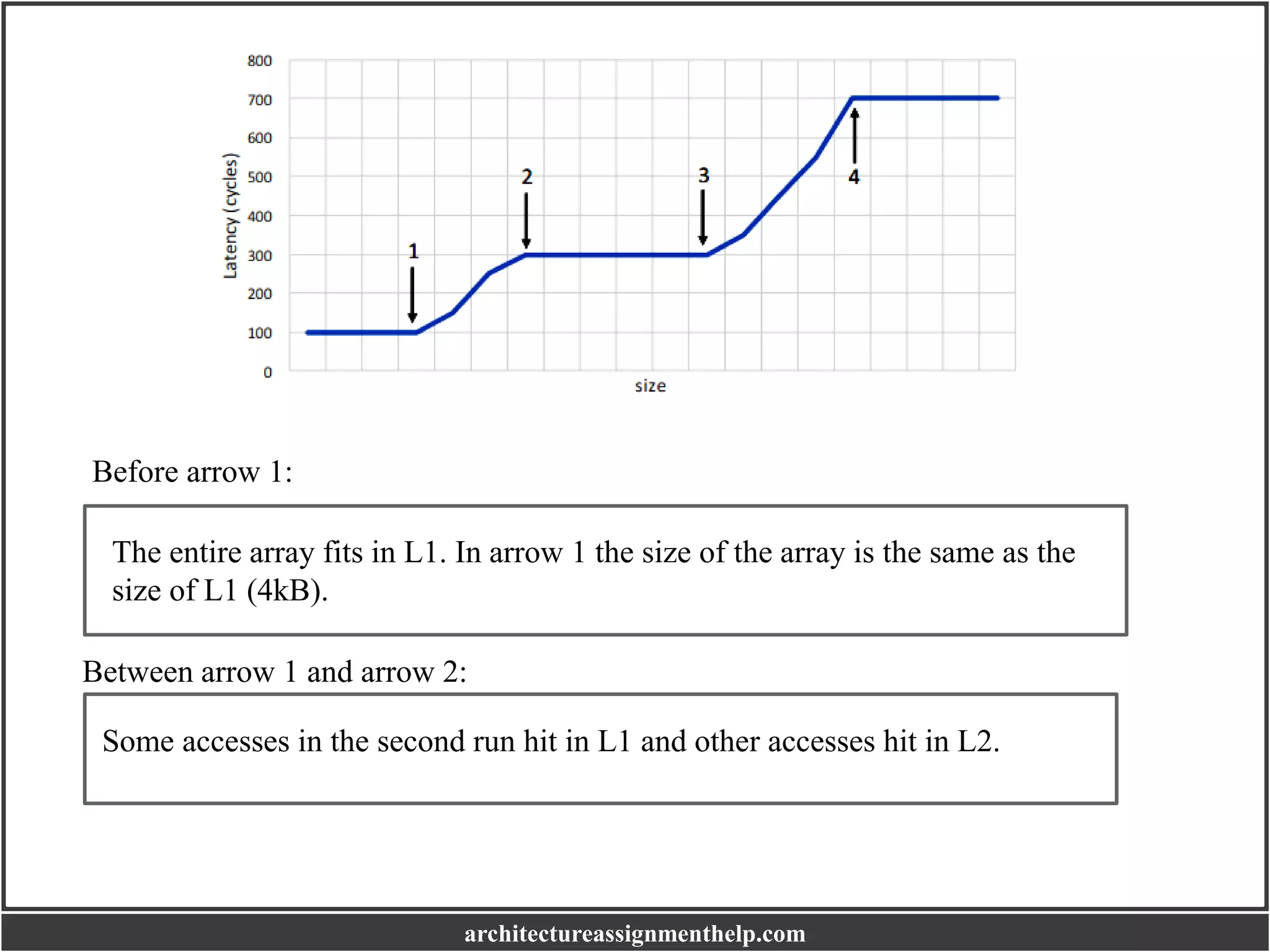
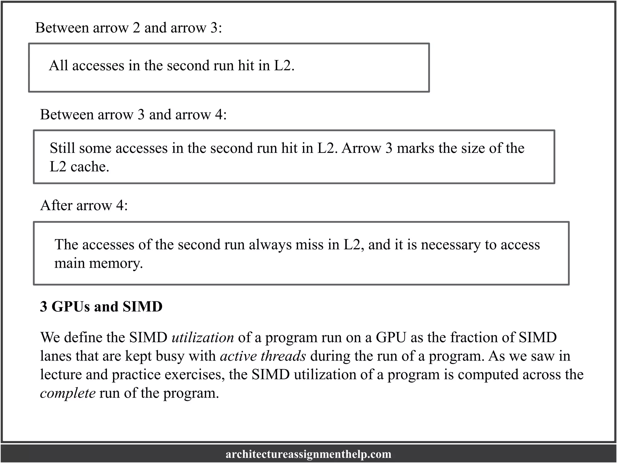
The cache hierarchy has two levels. L1 is a 4kB set associative cache.
(a) When we run code (1), we obtain the latency values in the following chart for the
first 64 reads to the array data (in the first 64 iterations of the loop) with stride equal to
1. What are the cache block sizes in L1 and L2?
architectureassignmenthelp.com](https://image.slidesharecdn.com/architectureassignmenthelp-220616050755-49527b24/75/Architecture-Assignment-Help-7-2048.jpg)
![L1 cache block size is 32 bytes, and L2 cache block size is 128 bytes.
Explanation: The highest latency values (700 cycles) correspond to L2 cache misses.
The latency of 300 cycles correspond to L1 cache misses that hit the L2 cache. The
lowest latency (100 cycles) corresponds to L1 cache hits. We find L1 misses every 8
32-bit elements, and L2 misses every 32 32-bit elements. Thus, L1 cache blocks are of
size 32 bytes, while L2 cache blocks are 128 bytes.
(b) Using code (2) with stride1 = stride2 = 32, size1 = 1056, and size2 = 1024,
we observe latency[0] = 300 cycles. However, if size1 = 1024, latency[0] = 100
cycles. What is the maximum number of ways in L1? (Note: The replacement policy
can be either FIFO or LRU).
The maximum number of ways is 32.
Explanation:
In L1 there are a total of 128 cache blocks. If the accessed space is 1056
elements, 33 cache blocks are read. In case of having more than 32 ways, there
would be a hit in the second loop. However, with 32 or less ways, the cache
block that contains data[0] is replaced in the last iteration of the first loop.
architectureassignmenthelp.com](https://image.slidesharecdn.com/architectureassignmenthelp-220616050755-49527b24/75/Architecture-Assignment-Help-8-2048.jpg)
![(c) We want to find out the exact replacement policy, assuming that the associativity is the
maximum obtained in part (b). We first run code (2) with stride1 = 32, size1 = 1024,
stride2 = 64, and size2 = 1056. Then (after resetting j), we run code (1) with stride = 32
and size = 1024. We observe latency[1] = 100 cycles. What is the replacement policy?
Explain. (Hint: The replacement policy can be either FIFO or LRU. You need to find the
correct one and explain).
It is FIFO.
Explanation:
In the second loop of code (2), the last cache block that is accessed (data[1024])
replaces the cache block that contains data[0], if the replacement policy is FIFO. If the
replacement policy is LRU, the LRU cache block (the one that contains data[32]).
Because we observe that latency[1] is 100 cycles, and it corresponds to the access to
data[32], we conclude the replacement policy is FIFO.
(d) Now we carry out two consecutive runs of code (1) for different values of size. In the
first run, stride is equal to 1. In the second run, stride is equal to 16. We ignore the
latency results of the first run, and average the latency results of the second run. We
obtain the following graph. What do the four parts shown with the arrows represent?
architectureassignmenthelp.com](https://image.slidesharecdn.com/architectureassignmenthelp-220616050755-49527b24/75/Architecture-Assignment-Help-9-2048.jpg)
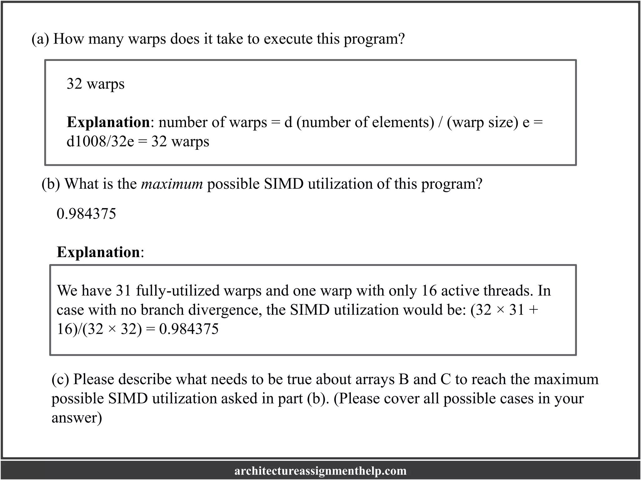
![The following code segment is run on a GPU. Each thread executes a single iteration of
the shown loop. Assume that the data values of the arrays A, B, and C are already in
vector registers, so there are no loads and stores in this program. (Hint: Notice that there
are 6 instructions in each thread.) A warp in the GPU consists of 32 threads, and there are
32 SIMD lanes in the GPU. Please assume that all values in arrays B and C have
magnitudes less than 10 (i.e., |B[i]| < 10 and |C[i]| < 10, for all i).
for (i = 0; i < 1008; i++) {
A[i] = B[i] * C[i];
if (A[i] < 0) {
C[i] = A[i] * B[i];
if (C[i] < 0) {
A[i] = A[i] + 1;
}
A[i] = A[i] - 2;
}
}
Please answer the following six questions.
architectureassignmenthelp.com](https://image.slidesharecdn.com/architectureassignmenthelp-220616050755-49527b24/75/Architecture-Assignment-Help-12-2048.jpg)
![For each 32 consecutive elements: ((B[i]==0 || C[i]==0) || (B[i] < 0 & C[i] < 0) || (B[i]
> 0 & C[i] > 0)) || ((B[i] < 0 & C[i] > 0) || (B[i] > 0 & C[i] < 0))
Explanation: We can have two possibilities: (1) No threads inside a warp take the
first "if". It is possible if for 32 consecutive elements, the following condition is true:
(B[i]==0 || C[i]==0) || (B[i] < 0 & C[i] < 0) || (B[i] > 0 & C[i] > 0)
(2) All threads inside a warp take the first "if". It is possible if for 32 consecutive
elements, the following condition is true:
(B[i] < 0 & C[i] > 0) || (B[i] > 0 & C[i] < 0) This condition also ensures that for the
second "if", all threads take the branch or no threads take the branch.
Finally, for every 32 consecutive elements, we should have one of the mentioned
possibilities. For the warp with 16 active threads, we should have one of mentioned
possibilities for every 16 consecutive elements
(d) What is the minimum possible SIMD utilization of this program?
architectureassignmenthelp.com](https://image.slidesharecdn.com/architectureassignmenthelp-220616050755-49527b24/75/Architecture-Assignment-Help-14-2048.jpg)
![((32+32+4)×31+16+16+4)/(32×6×32)=0.3489
Explanation:
The first two lines must be executed by every thread in a warp. The minimum
utilization results when a single thread from each warp passes both conditions, and
every other thread fails to meet the condition on the first "if". The thread per warp
that meets both conditions, executes four instructions.
(e) Please describe what needs to be true about arrays B and C to reach the minimum
possible SIMD utilization asked in part (d). (Please cover all possible cases in your
answer)
Exactly 1 of every 32 consecutive elements in arrays B and C should have this
condition: B[i] > 0 & C[i] < 0
Explanation: Only one thread in a warp should pass the first condition. Therefore,
exactly 1 of every 32 consecutive elements in arrays B and C should have the
following condition:
(B[i] < 0 & C[i] > 0) || (B[i] > 0 & C[i] < 0)
architectureassignmenthelp.com](https://image.slidesharecdn.com/architectureassignmenthelp-220616050755-49527b24/75/Architecture-Assignment-Help-15-2048.jpg)
![However, the thread in a warp which passes the first condition should also pass the
second condition. Therefore, the only condition which ensures the minimum possible
SIMD utilization is: exactly 1 of every 32 consecutive elements in arrays B and C
should have this condition: B[i] > 0 & C[i] < 0. For the warp with 16 active threads,
this condition should be true for exactly 1 of the 16 elements.
(f) Now consider a GPU that employs Dynamic Warp Formation (DWF) to improve the
SIMD utilization. As we discussed in the class, DWF dynamically merges threads
executing the same instruction (after branch divergence). What is the maximum
achievable SIMD utilization using DWF? Explain your answer (Hint: The maximum
SIMD utilization can happen under the conditions you found in part (e)).
((32+32)×31+16+16+32×4)/((32+32)×32+32×4) = 0.985
Explanation: DWF can ideally merge 32 warps with only one active threads in
a single warp. This could be happen if none of the threads inside the warp have
overlaps. If it happens, we will run 31 fully utilized warps and one warp with
16 active threads for the first and second instructions. Then, we will have only
one fully-utilized warp which executes the remaining 4 instructions.
architectureassignmenthelp.com](https://image.slidesharecdn.com/architectureassignmenthelp-220616050755-49527b24/75/Architecture-Assignment-Help-16-2048.jpg)

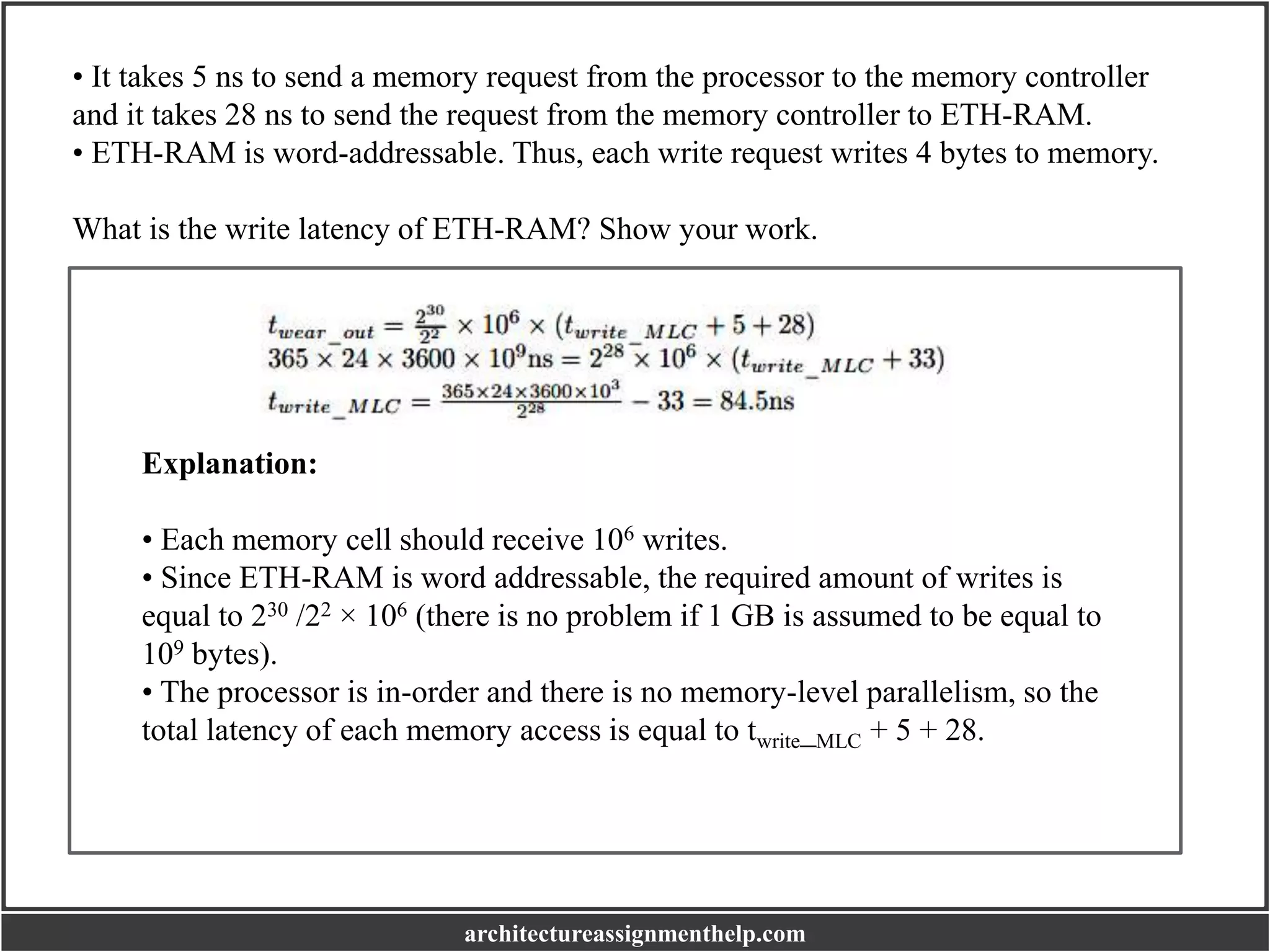
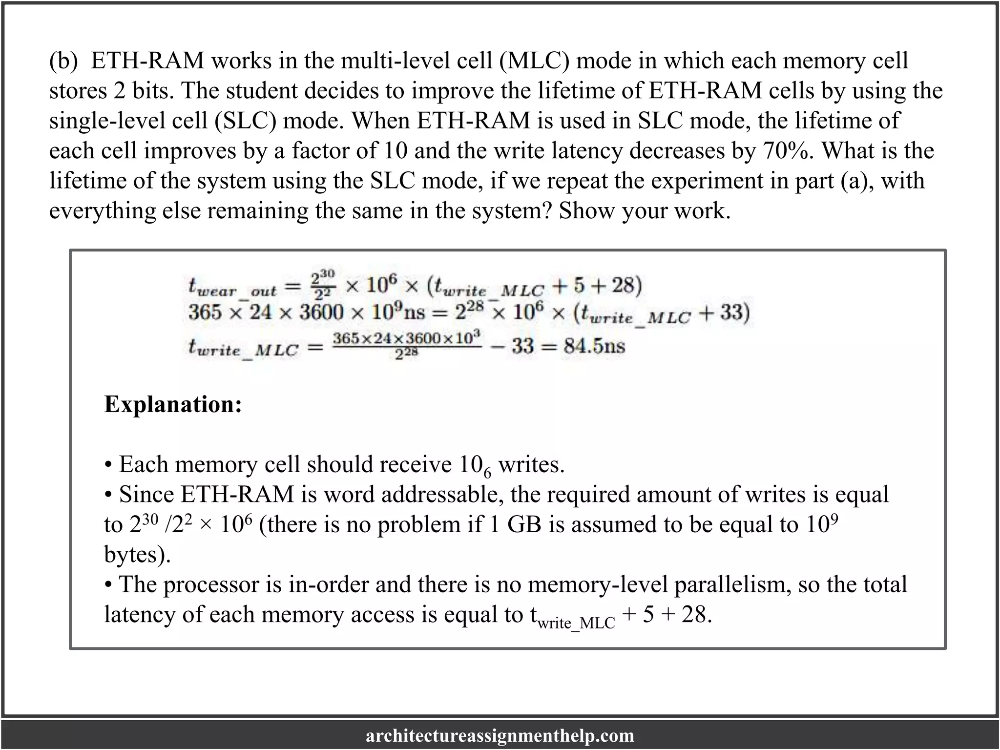
The document discusses emerging memory technology ETH-RAM developed at ETH Zurich, highlighting its features and endurance issues. A student created a computer system using 1 GB of ETH-RAM, which lasts one year with continuous writing. It also contrasts the performance and longevity of ETH-RAM in multi-level cell (MLC) and single-level cell (SLC) modes, alongside a cache performance analysis and GPU utilization metrics.