This document describes a mixed-mode PIDA controller circuit employing OTAs. It introduces PID and PIDA controllers and discusses their limitations. It then presents the proposed mixed-mode PIDA controller circuit design using OTAs which allows for either current or voltage input/output signals and independent adjustment of gain parameters. Simulation results show the circuit performs as theoretically expected with good agreement between ideal and simulated frequency responses. The circuit offers advantages over conventional controller designs and can be applied in closed-loop control systems.
![The proportional-integral-derivative-acceleration(PIDA)
controller
The proportional-integral-derivative-acceleration (PIDA)
controller [2] was proposed for a third order plant.](https://image.slidesharecdn.com/amixed-modepidacontrolleremployingotas-231026091802-28bb2fa1/85/A-mixed-mode-PIDA-controller-employing-OTAs-pptx-4-320.jpg)
![THE SYNTHESIS OF ELECTRONIC CONTROLLER
CIRCUITS
using op-amp and passive element [3]-[4], they consume
high power and their frequency response is limited by
GBP](https://image.slidesharecdn.com/amixed-modepidacontrolleremployingotas-231026091802-28bb2fa1/85/A-mixed-mode-PIDA-controller-employing-OTAs-pptx-5-320.jpg)
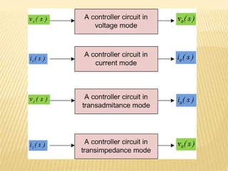
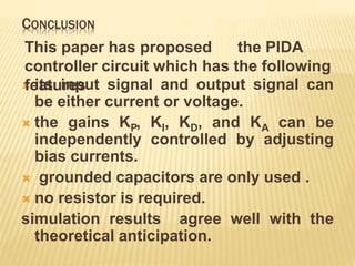
![ PIDA circuits using OTA (Operational
Transconductance Amplifier), CFOA
(Current Feedback Operational Amplifier),
and CCII (second generation current
conveyor) were proposed [5], [6], and [7].
This controller is more advantageous than
conventional controllers.
Since the inputs and output of proposed
controller can be either current signal or
voltage signal, the application of circuitry
will be more flexible](https://image.slidesharecdn.com/amixed-modepidacontrolleremployingotas-231026091802-28bb2fa1/85/A-mixed-mode-PIDA-controller-employing-OTAs-pptx-6-320.jpg)