K. Webb ECE322
29
Diode Models
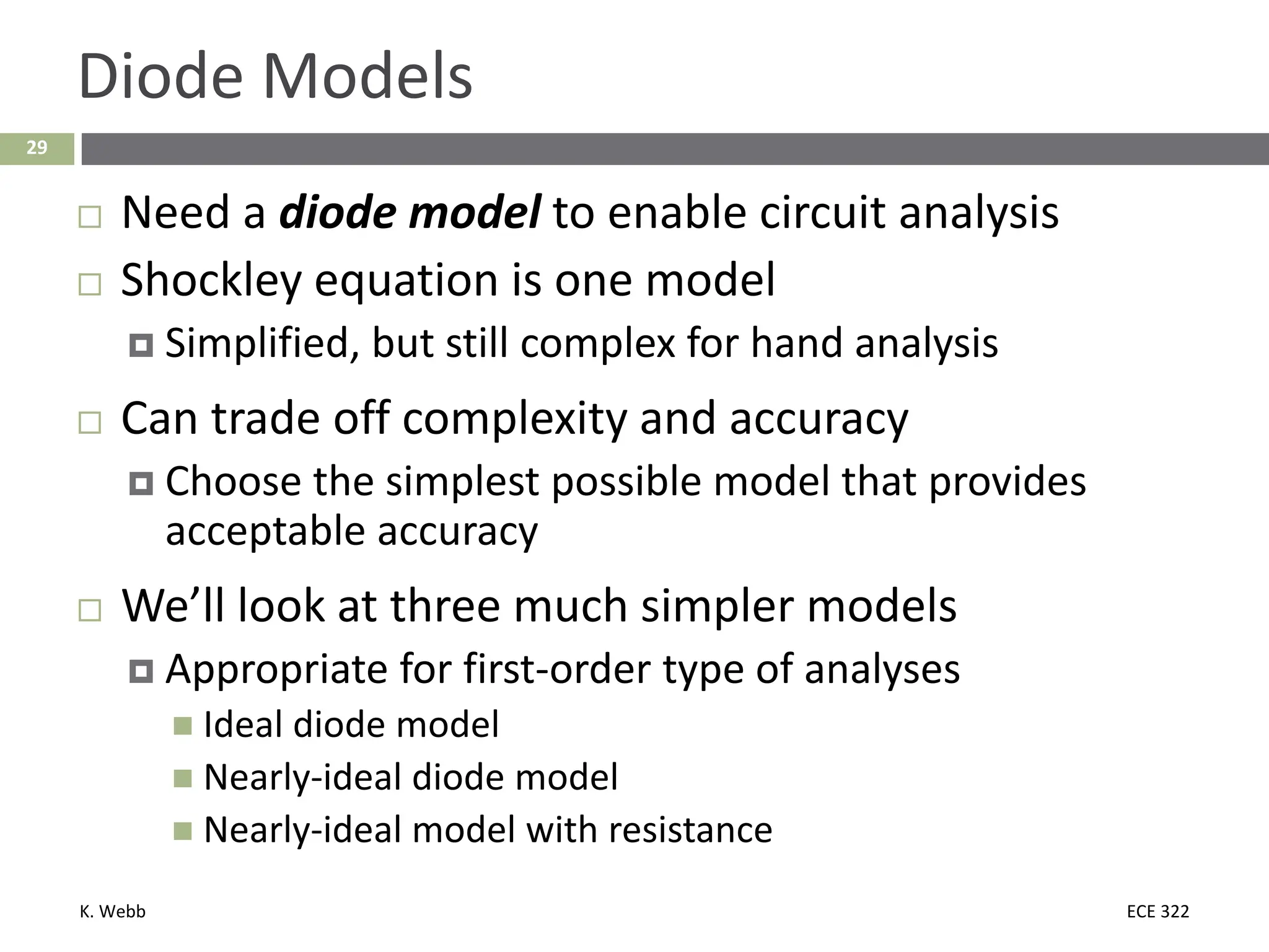
Need a diode model to enable circuit analysis
Shockley equation is one model
Simplified, but still complex for hand analysis
Can trade off complexity and accuracy
Choose the simplest possible model that provides
acceptable accuracy
We’ll look at three much simpler models
Appropriate for first-order type of analyses
Ideal diode model
Nearly-ideal diode model
Nearly-ideal model with resistance
3.
K. Webb ECE322
30
Ideal Diode Model
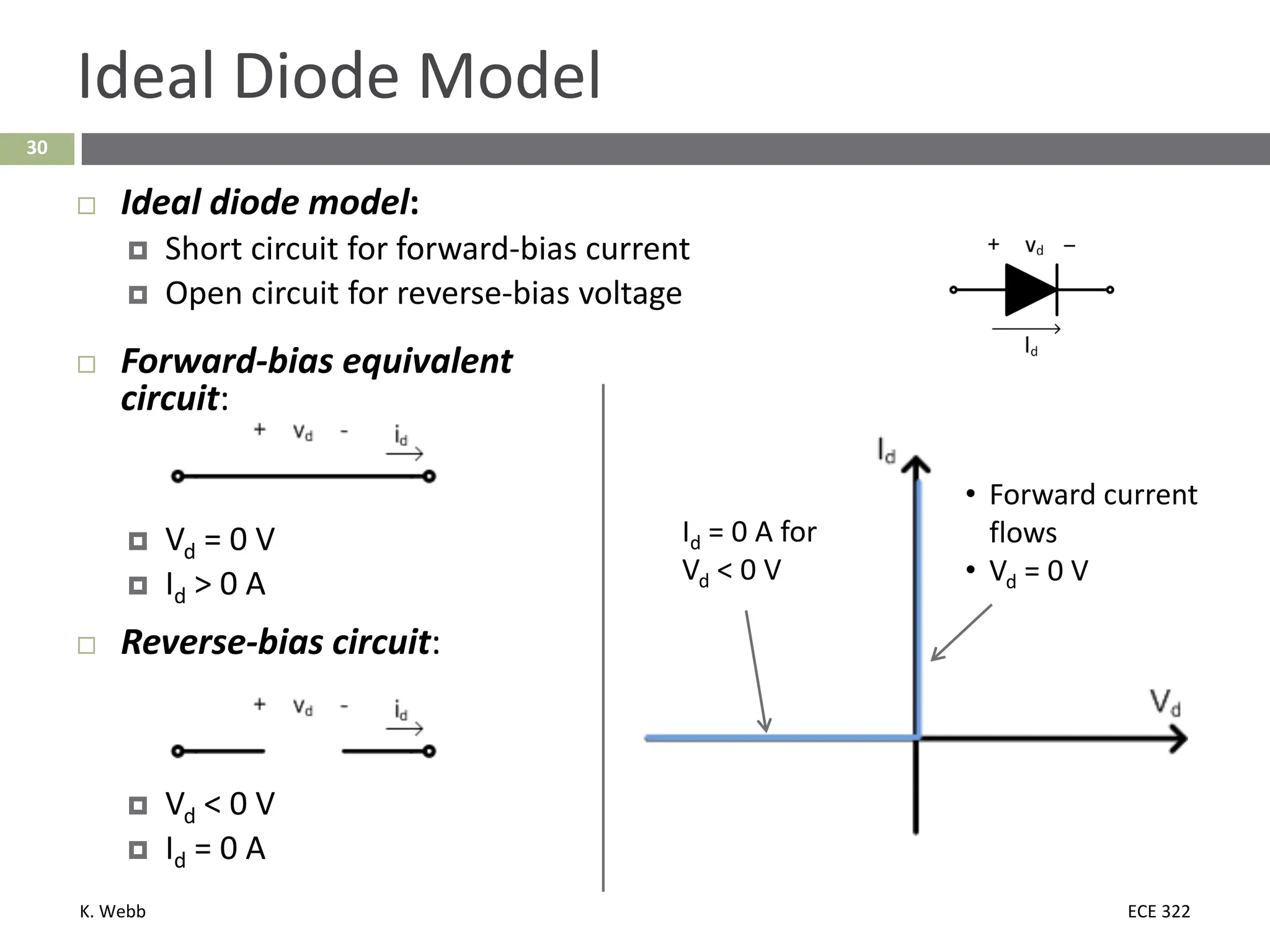
Ideal diode model:
Short circuit for forward-bias current
Open circuit for reverse-bias voltage
Id = 0 A for
Vd < 0 V
• Forward current
flows
• Vd = 0 V
Forward-bias equivalent
circuit:
Vd = 0 V
Id > 0 A
Reverse-bias circuit:
Vd < 0 V
Id = 0 A
4.
K. Webb ECE322
31
Nearly-Ideal Diode Model
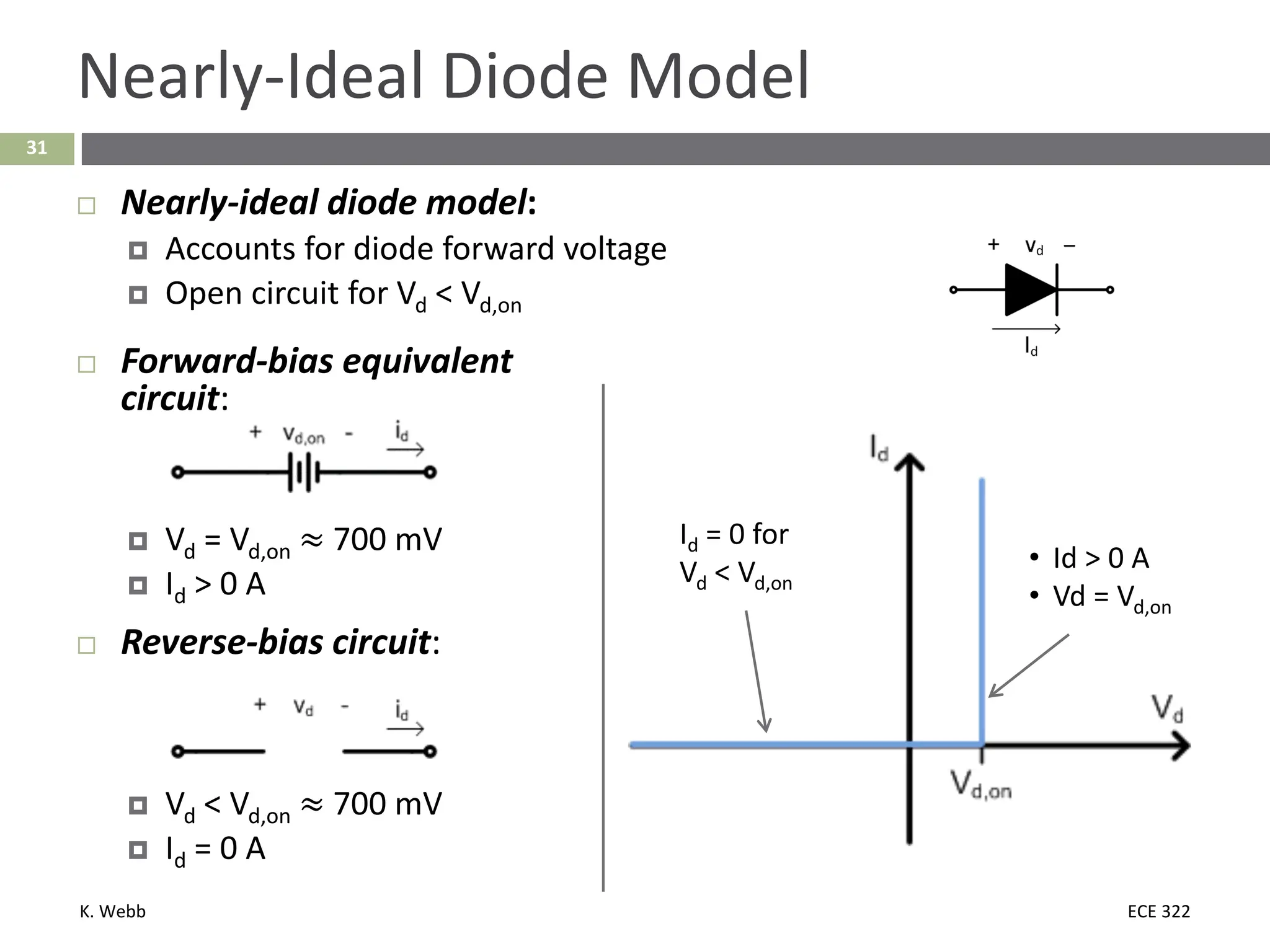
Nearly-ideal diode model:
Accounts for diode forward voltage
Open circuit for Vd < Vd,on
Forward-bias equivalent
circuit:
Vd = Vd,on ≈ 700 mV
Id > 0 A
Reverse-bias circuit:
Vd < Vd,on ≈ 700 mV
Id = 0 A
Id = 0 for
Vd < Vd,on
• Id > 0 A
• Vd = Vd,on
5.
K. Webb ECE322
32
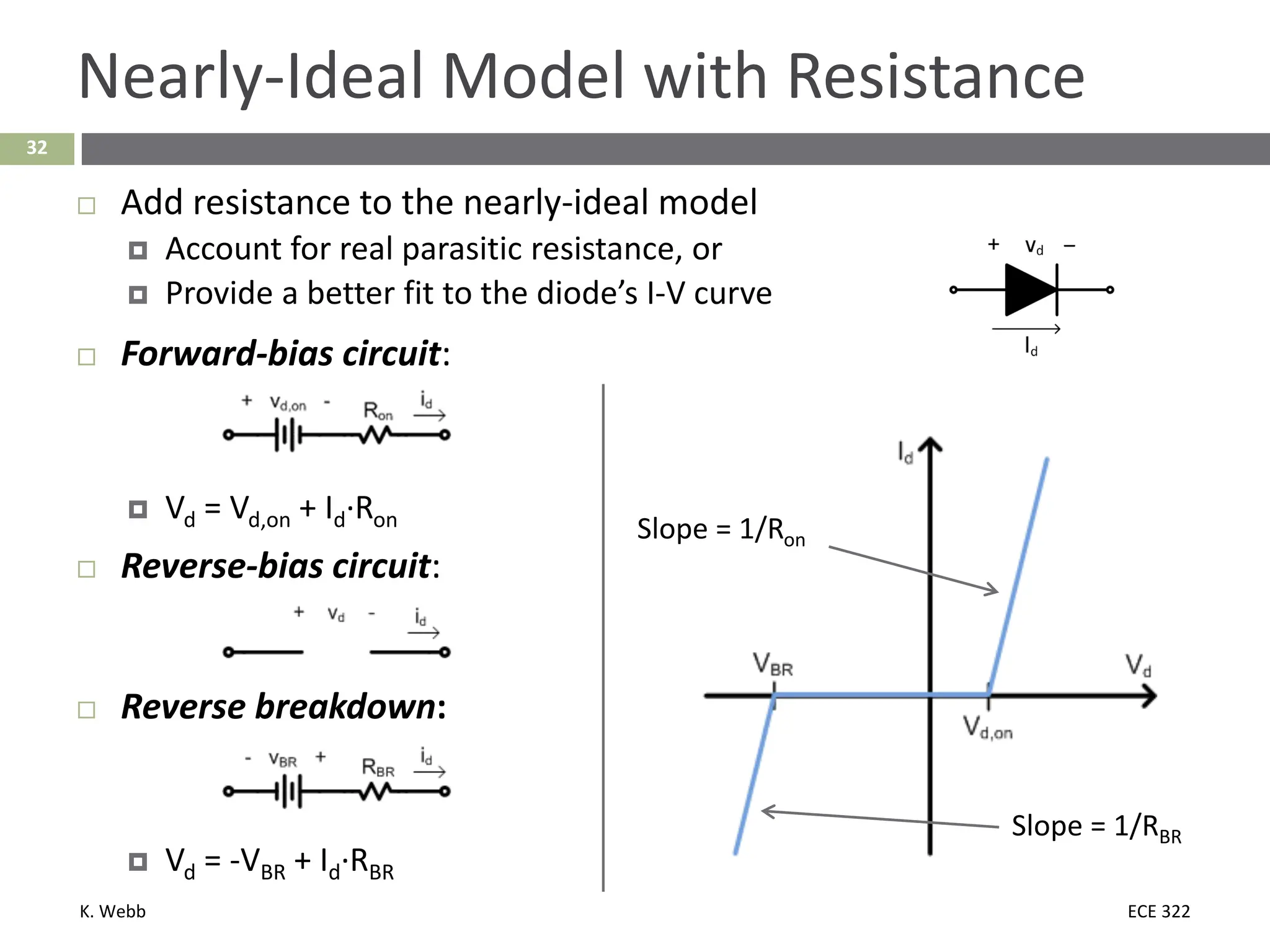
Nearly-Ideal Model with Resistance
Add resistance to the nearly-ideal model
Account for real parasitic resistance, or
Provide a better fit to the diode’s I-V curve
Forward-bias circuit:
Vd = Vd,on + Id∙Ron
Reverse-bias circuit:
Reverse breakdown:
Vd = -VBR + Id∙RBR
Slope = 1/Ron
Slope = 1/RBR
K. Webb ECE322
34
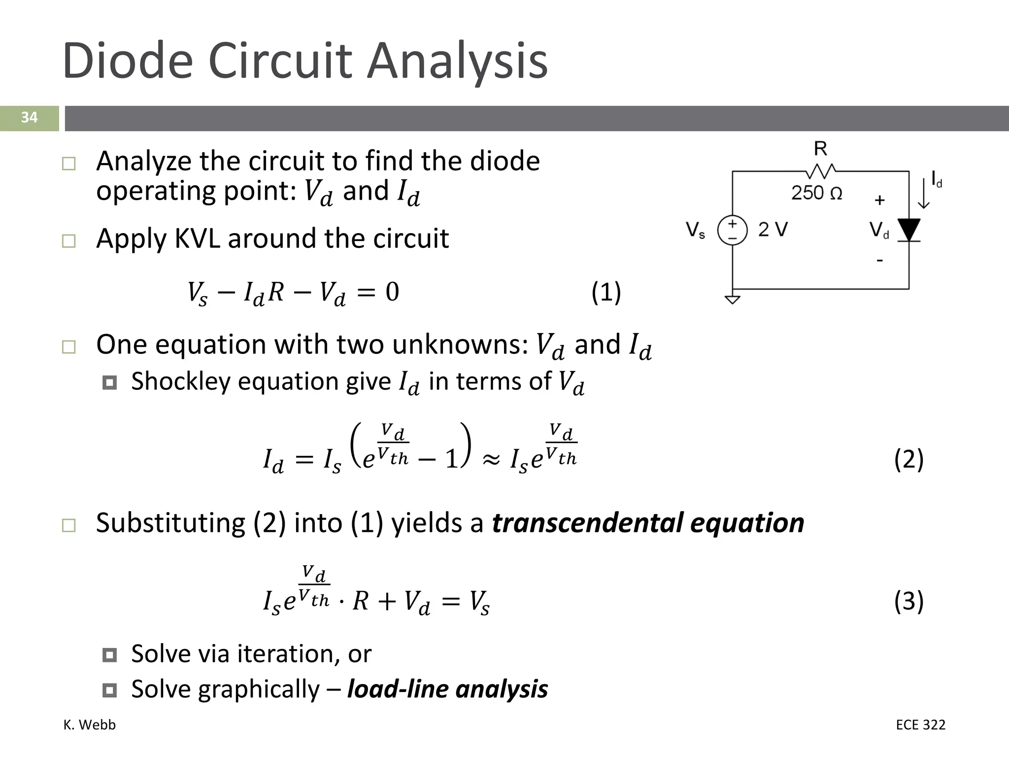
Diode Circuit Analysis
Analyze the circuit to find the diode
operating point: 𝑉𝑉𝑑𝑑 and 𝐼𝐼𝑑𝑑
Apply KVL around the circuit
𝑉𝑉
𝑠𝑠 − 𝐼𝐼𝑑𝑑𝑅𝑅 − 𝑉𝑉𝑑𝑑 = 0 (1)
One equation with two unknowns: 𝑉𝑉𝑑𝑑 and 𝐼𝐼𝑑𝑑
Shockley equation give 𝐼𝐼𝑑𝑑 in terms of 𝑉𝑉𝑑𝑑
𝐼𝐼𝑑𝑑 = 𝐼𝐼𝑠𝑠 𝑒𝑒
𝑉𝑉𝑑𝑑
𝑉𝑉𝑡𝑡𝑡 − 1 ≈ 𝐼𝐼𝑠𝑠𝑒𝑒
𝑉𝑉𝑑𝑑
𝑉𝑉𝑡𝑡𝑡 (2)
Substituting (2) into (1) yields a transcendental equation
𝐼𝐼𝑠𝑠𝑒𝑒
𝑉𝑉𝑑𝑑
𝑉𝑉𝑡𝑡𝑡 ⋅ 𝑅𝑅 + 𝑉𝑉𝑑𝑑 = 𝑉𝑉
𝑠𝑠 (3)
Solve via iteration, or
Solve graphically – load-line analysis
8.
K. Webb ECE322
35
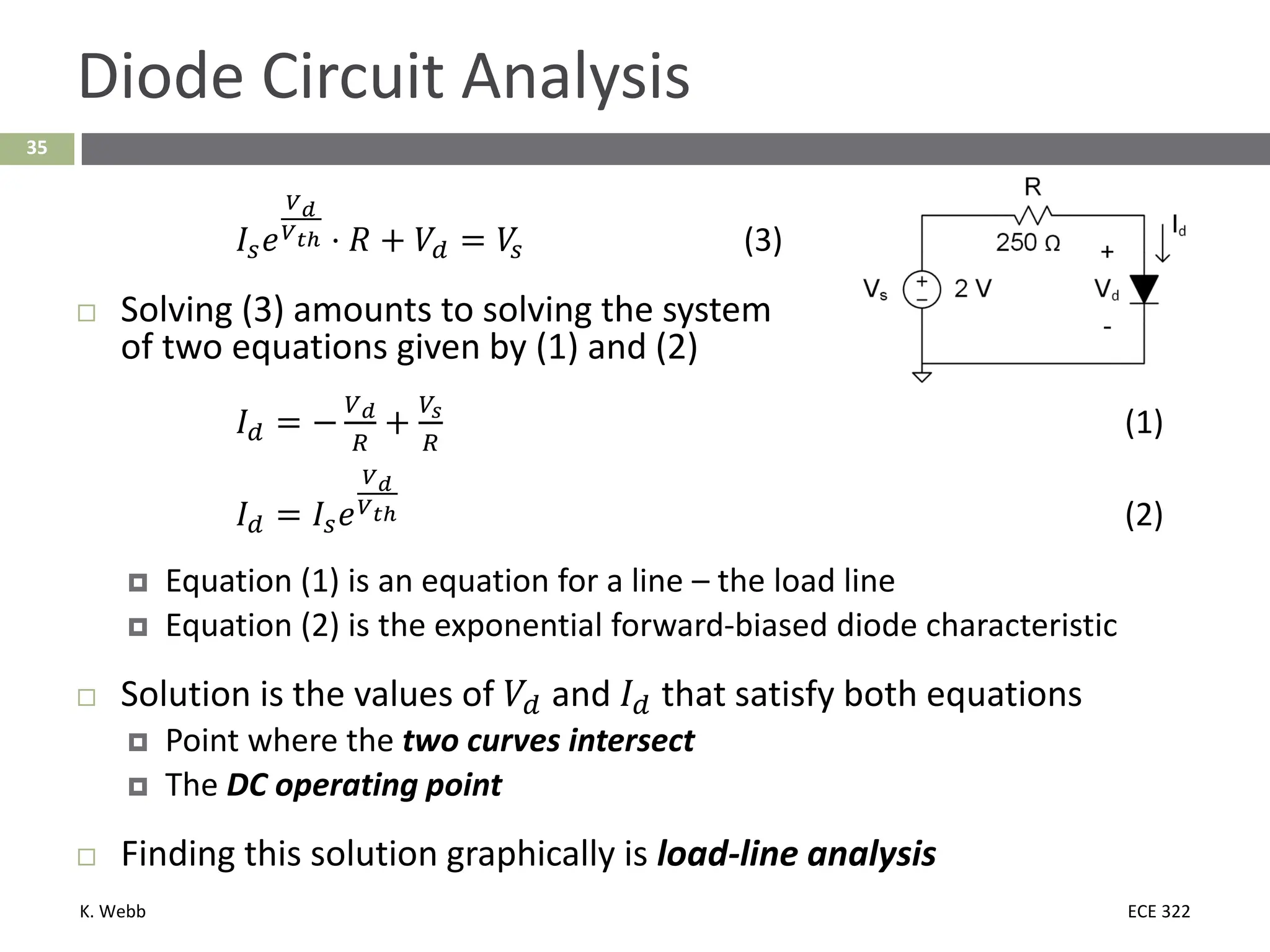
Diode Circuit Analysis
𝐼𝐼𝑠𝑠𝑒𝑒
𝑉𝑉𝑑𝑑
𝑉𝑉𝑡𝑡𝑡 ⋅ 𝑅𝑅 + 𝑉𝑉𝑑𝑑 = 𝑉𝑉
𝑠𝑠 (3)
Solving (3) amounts to solving the system
of two equations given by (1) and (2)
𝐼𝐼𝑑𝑑 = −
𝑉𝑉𝑑𝑑
𝑅𝑅
+
𝑉𝑉𝑠𝑠
𝑅𝑅
(1)
𝐼𝐼𝑑𝑑 = 𝐼𝐼𝑠𝑠𝑒𝑒
𝑉𝑉𝑑𝑑
𝑉𝑉𝑡𝑡𝑡 (2)
Equation (1) is an equation for a line – the load line
Equation (2) is the exponential forward-biased diode characteristic
Solution is the values of 𝑉𝑉𝑑𝑑 and 𝐼𝐼𝑑𝑑 that satisfy both equations
Point where the two curves intersect
The DC operating point
Finding this solution graphically is load-line analysis
9.
K. Webb ECE322
36
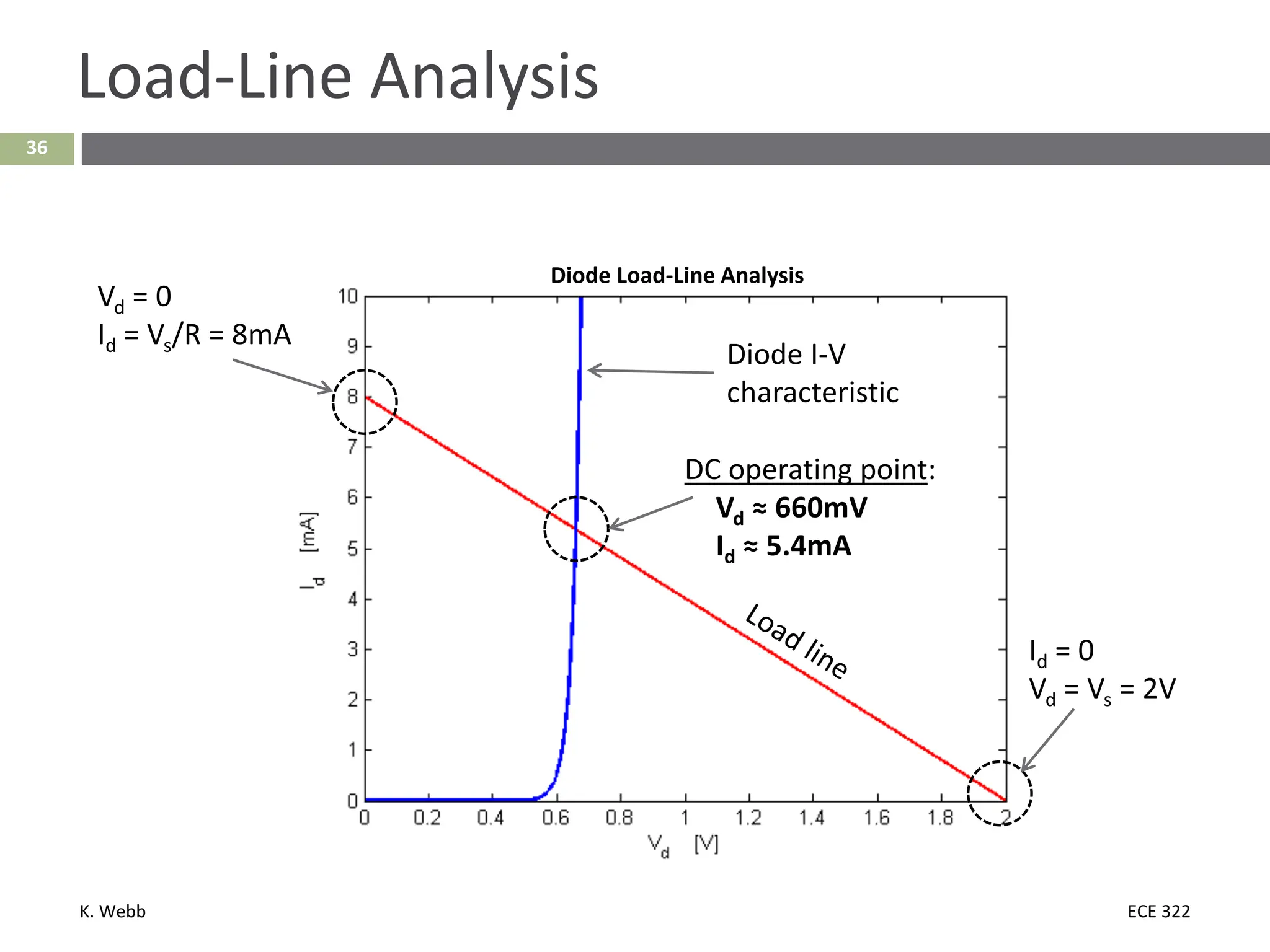
Load-Line Analysis
Diode I-V
characteristic
DC operating point:
Vd ≈ 660mV
Id ≈ 5.4mA
Id = 0
Vd = Vs = 2V
Vd = 0
Id = Vs/R = 8mA
Diode Load-Line Analysis
10.
K. Webb ECE322
Analysis with Simple Diode Models
37
11.
K. Webb ECE322
38
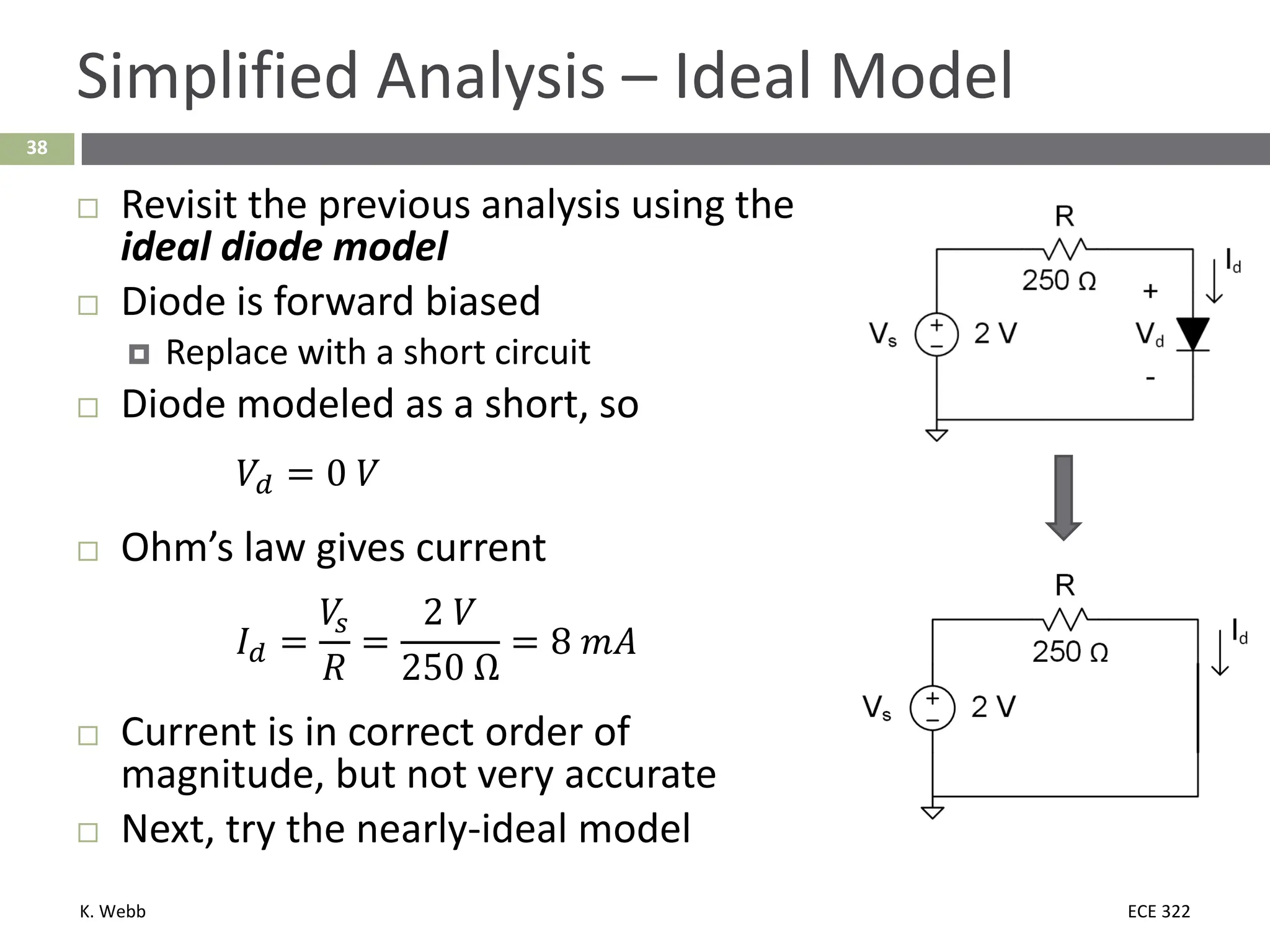
Simplified Analysis – Ideal Model
Revisit the previous analysis using the
ideal diode model
Diode is forward biased
Replace with a short circuit
Diode modeled as a short, so
𝑉𝑉𝑑𝑑 = 0 𝑉𝑉
Ohm’s law gives current
𝐼𝐼𝑑𝑑 =
𝑉𝑉
𝑠𝑠
𝑅𝑅
=
2 𝑉𝑉
250 Ω
= 8 𝑚𝑚𝑝𝑝
Current is in correct order of
magnitude, but not very accurate
Next, try the nearly-ideal model
12.
K. Webb ECE322
39
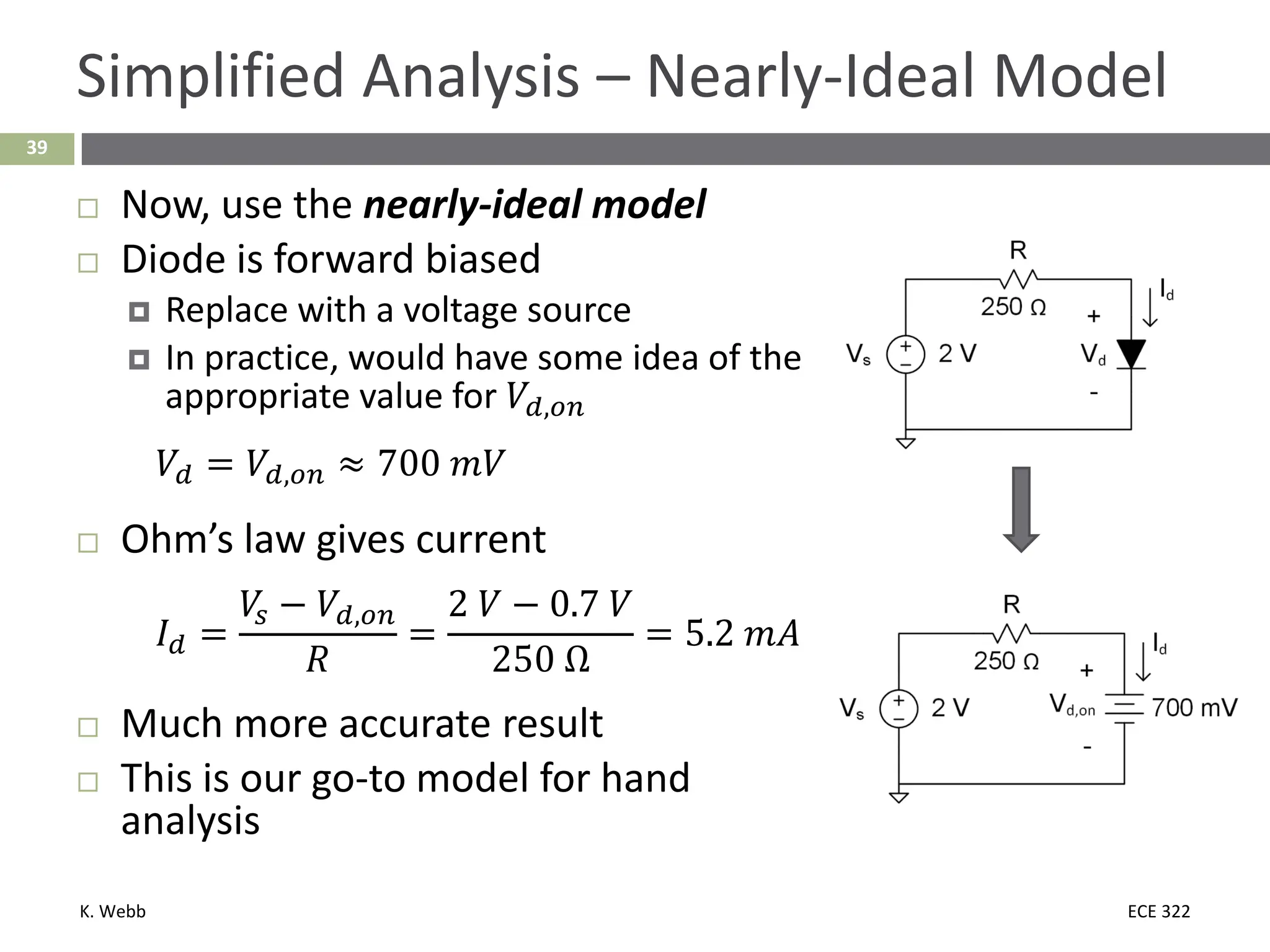
Simplified Analysis – Nearly-Ideal Model
Now, use the nearly-ideal model
Diode is forward biased
Replace with a voltage source
In practice, would have some idea of the
appropriate value for 𝑉𝑉𝑑𝑑,𝑜𝑜𝑜𝑜
𝑉𝑉𝑑𝑑 = 𝑉𝑉𝑑𝑑,𝑜𝑜𝑜𝑜 ≈ 700 𝑚𝑚𝑉𝑉
Ohm’s law gives current
𝐼𝐼𝑑𝑑 =
𝑉𝑉
𝑠𝑠 − 𝑉𝑉𝑑𝑑,𝑜𝑜𝑜𝑜
𝑅𝑅
=
2 𝑉𝑉 − 0.7 𝑉𝑉
250 Ω
= 5.2 𝑚𝑚𝑝𝑝
Much more accurate result
This is our go-to model for hand
analysis
K. Webb ECE322
41
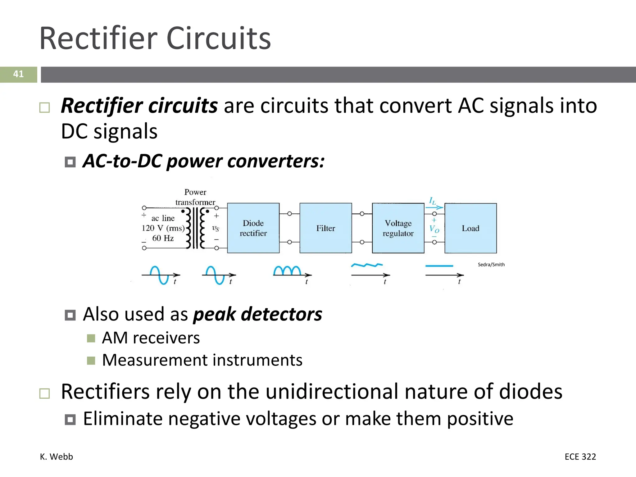
Rectifier Circuits
Rectifier circuits are circuits that convert AC signals into
DC signals
AC-to-DC power converters:
Also used as peak detectors
AM receivers
Measurement instruments
Rectifiers rely on the unidirectional nature of diodes
Eliminate negative voltages or make them positive
Sedra/Smith
K. Webb ECE322
44
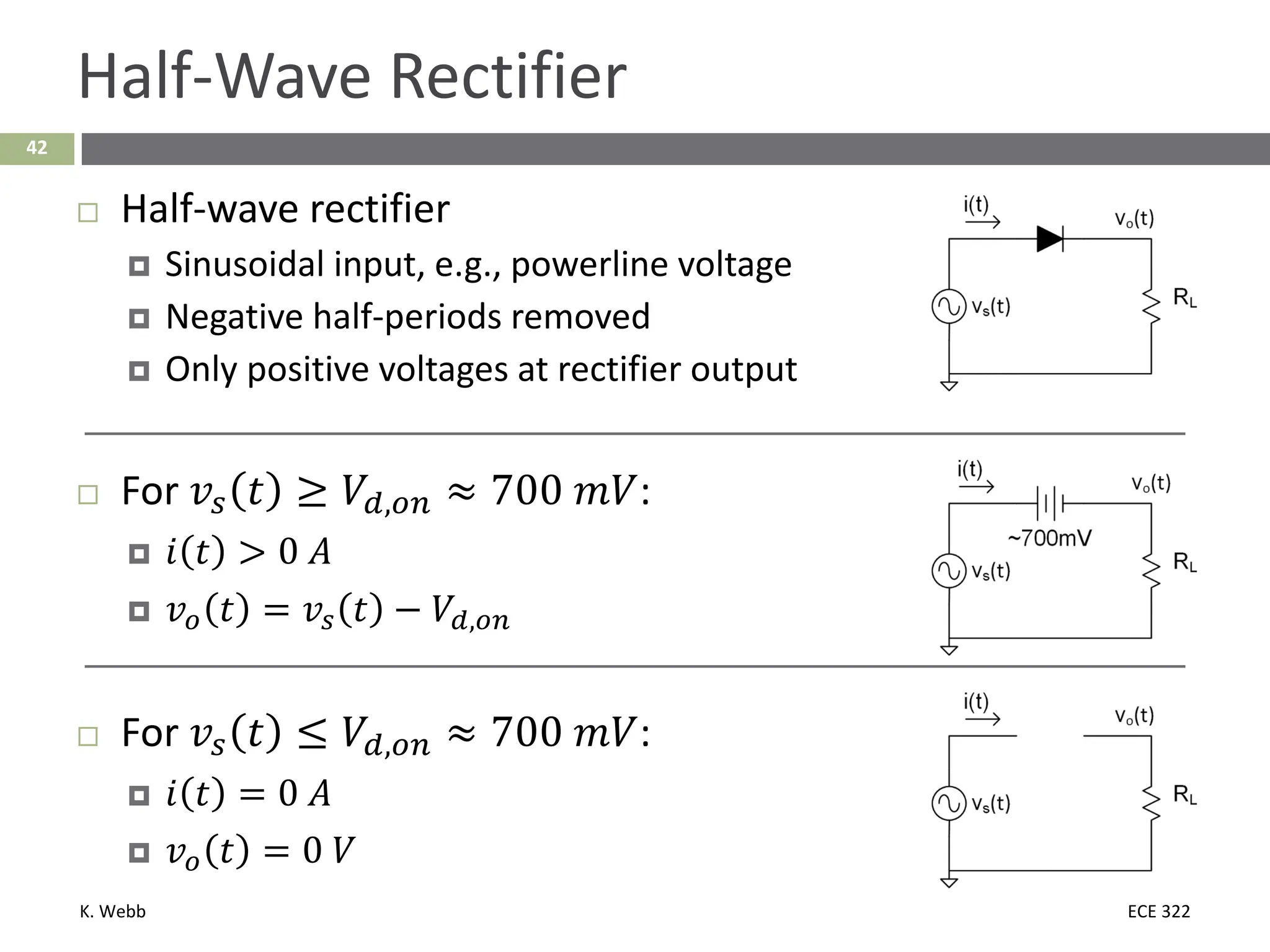
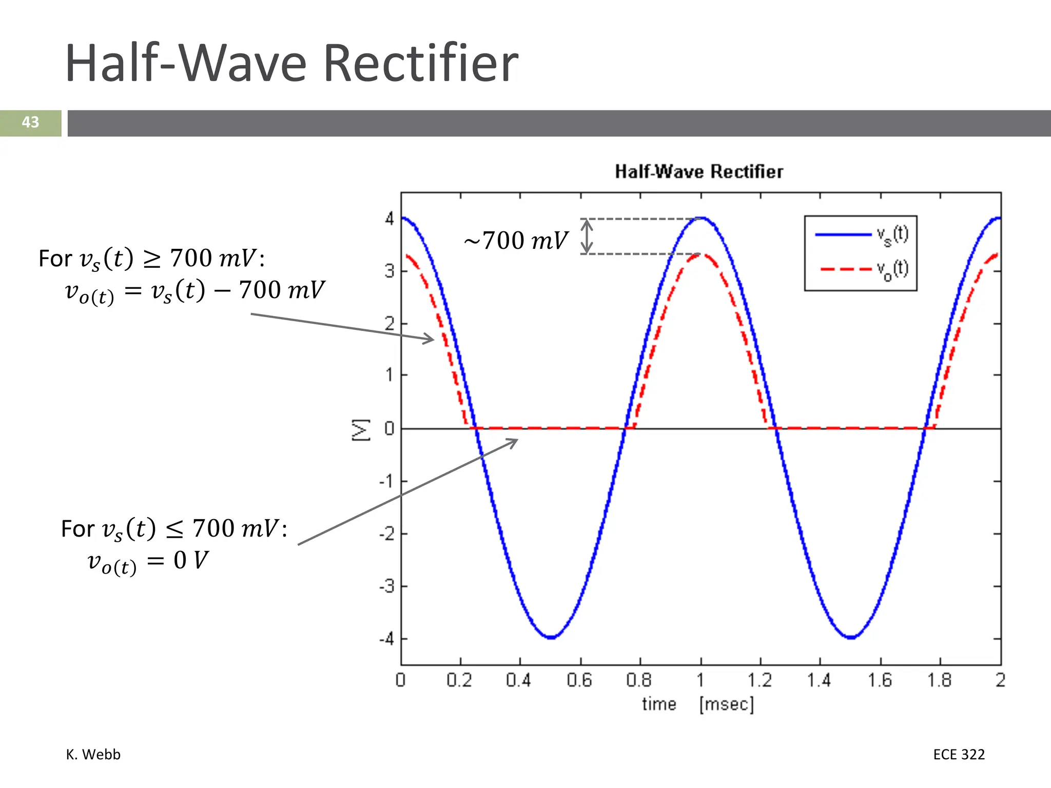
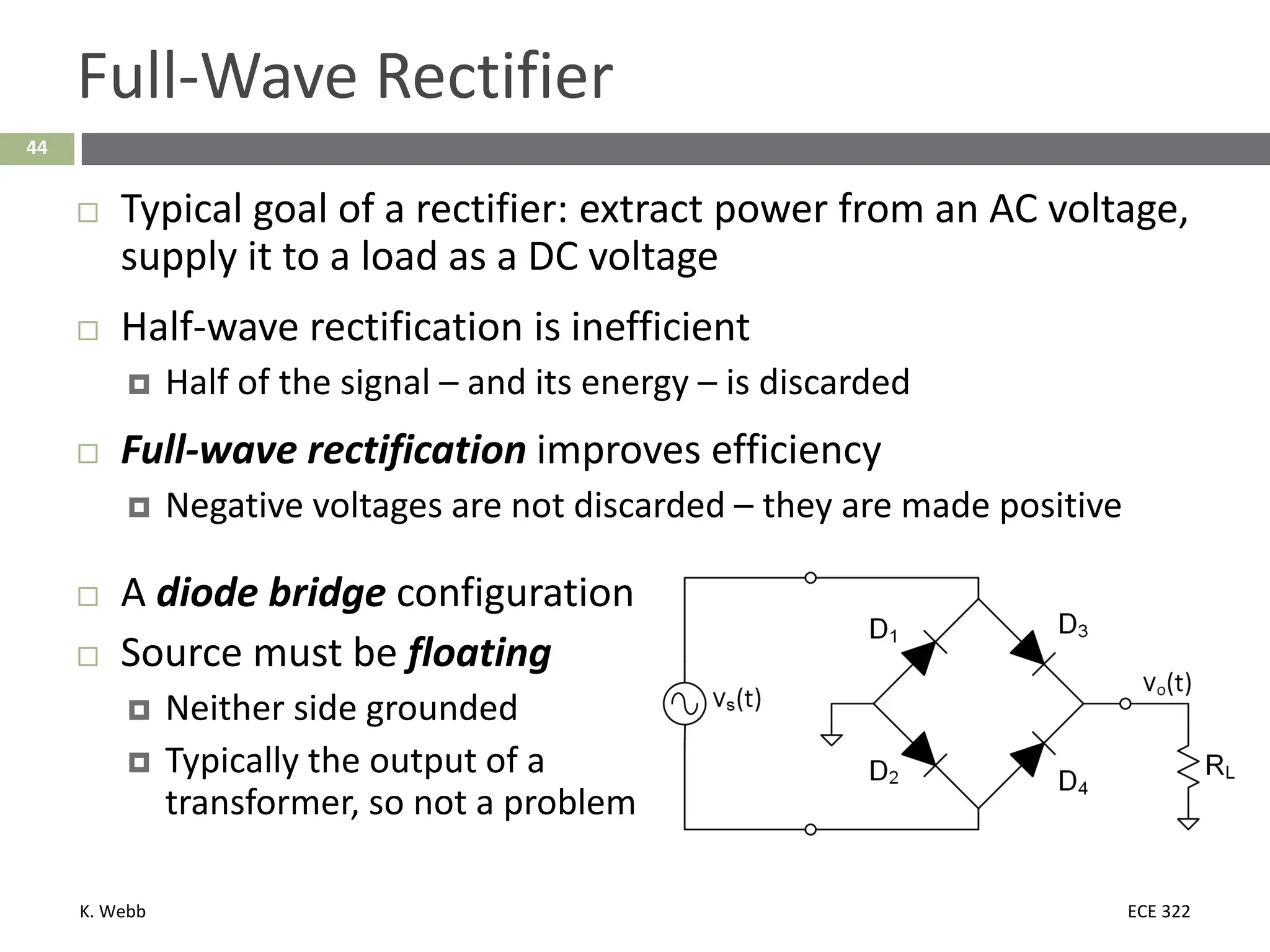
Full-Wave Rectifier
Typical goal of a rectifier: extract power from an AC voltage,
supply it to a load as a DC voltage
Half-wave rectification is inefficient
Half of the signal – and its energy – is discarded
Full-wave rectification improves efficiency
Negative voltages are not discarded – they are made positive
A diode bridge configuration
Source must be floating
Neither side grounded
Typically the output of a
transformer, so not a problem
18.
K. Webb ECE322
45
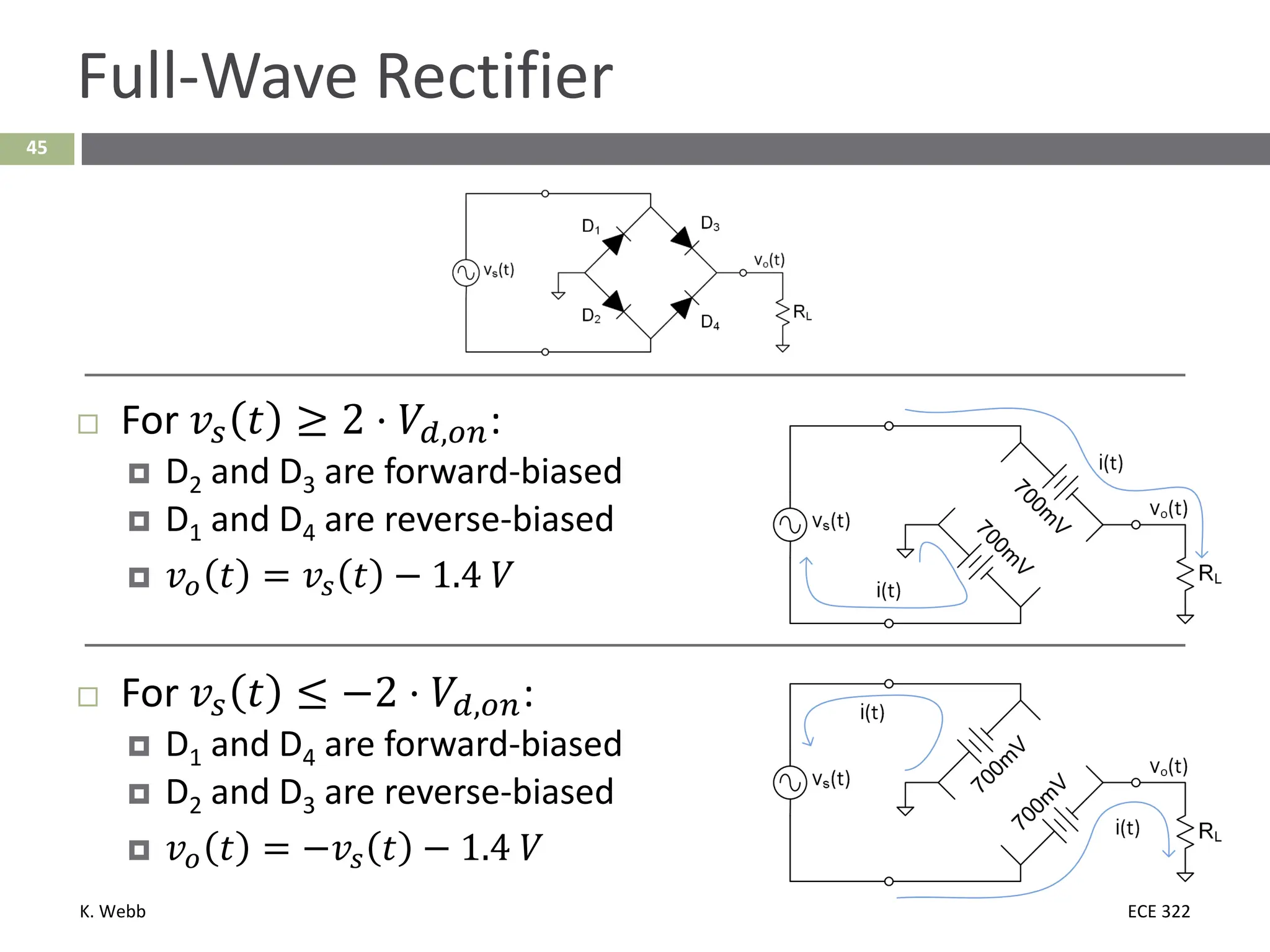
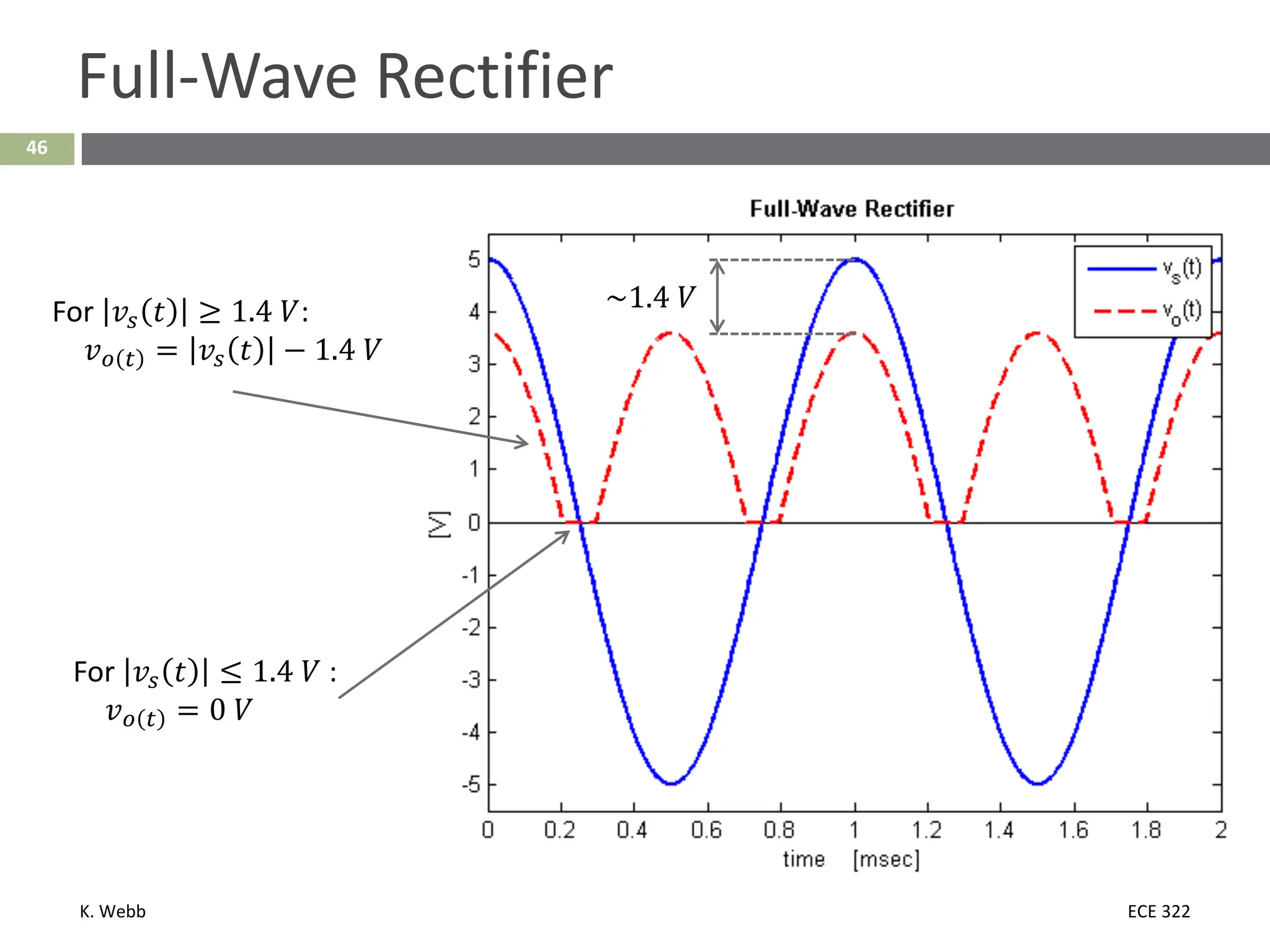
Full-Wave Rectifier
For 𝑣𝑣𝑠𝑠 𝑡𝑡 ≥ 2 ⋅ 𝑉𝑉𝑑𝑑,𝑜𝑜𝑜𝑜:
D2 and D3 are forward-biased
D1 and D4 are reverse-biased
𝑣𝑣𝑜𝑜 𝑡𝑡 = 𝑣𝑣𝑠𝑠 𝑡𝑡 − 1.4 𝑉𝑉
For 𝑣𝑣𝑠𝑠 𝑡𝑡 ≤ −2 ⋅ 𝑉𝑉𝑑𝑑,𝑜𝑜𝑜𝑜:
D1 and D4 are forward-biased
D2 and D3 are reverse-biased
𝑣𝑣𝑜𝑜 𝑡𝑡 = −𝑣𝑣𝑠𝑠 𝑡𝑡 − 1.4 𝑉𝑉
K. Webb ECE322
47
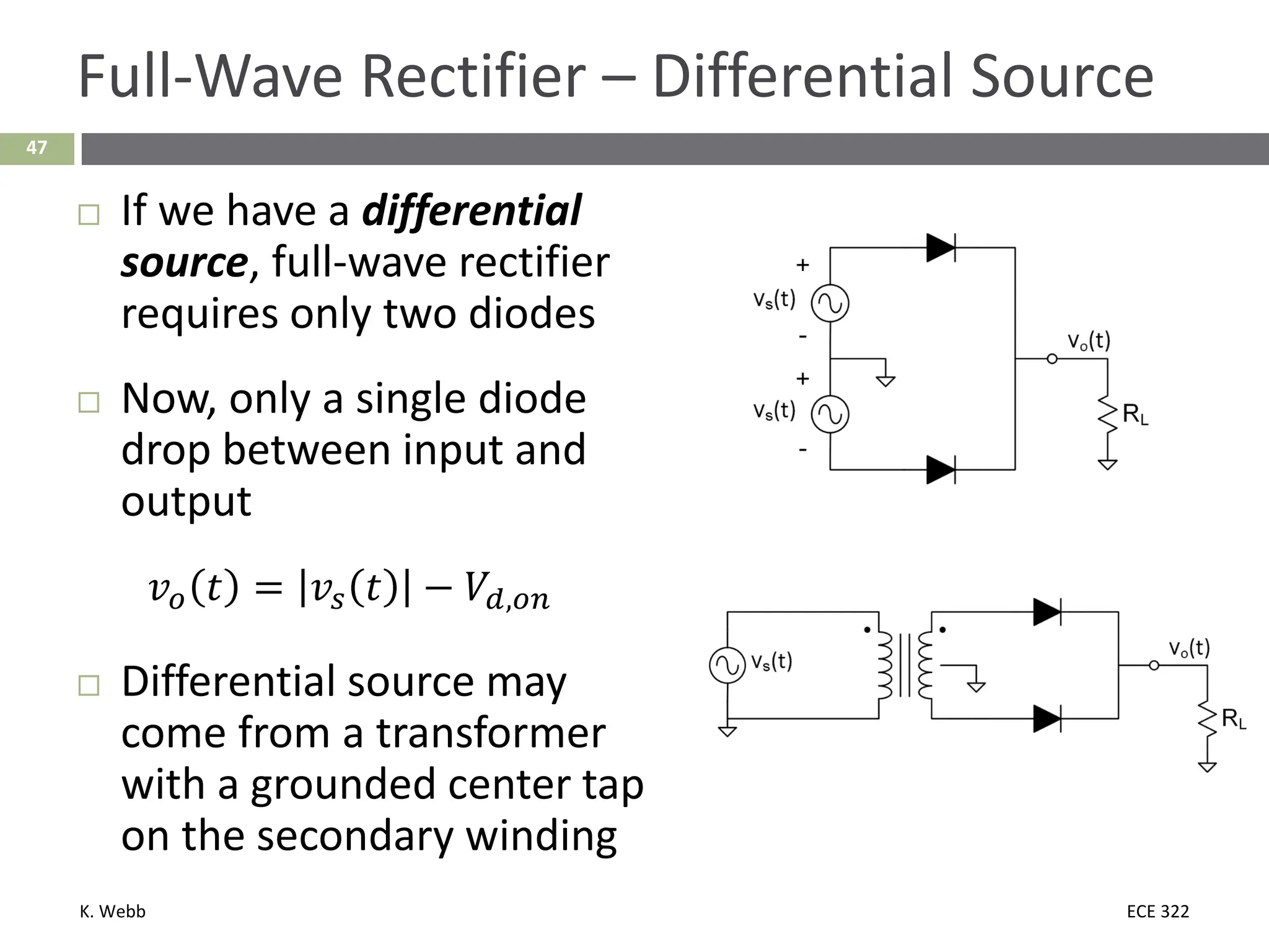
Full-Wave Rectifier – Differential Source
If we have a differential
source, full-wave rectifier
requires only two diodes
Now, only a single diode
drop between input and
output
𝑣𝑣𝑜𝑜 𝑡𝑡 = 𝑣𝑣𝑠𝑠 𝑡𝑡 − 𝑉𝑉𝑑𝑑,𝑜𝑜𝑜𝑜
Differential source may
come from a transformer
with a grounded center tap
on the secondary winding
21.
K. Webb ECE322
48
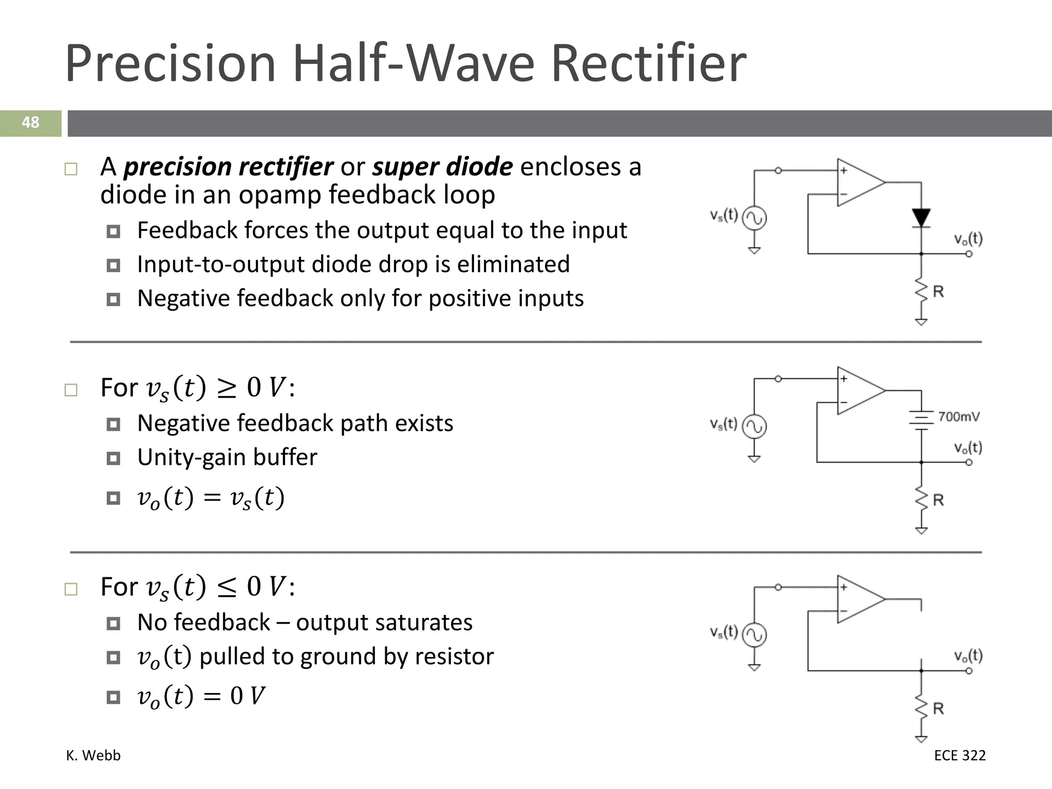
Precision Half-Wave Rectifier
A precision rectifier or super diode encloses a
diode in an opamp feedback loop
Feedback forces the output equal to the input
Input-to-output diode drop is eliminated
Negative feedback only for positive inputs
For 𝑣𝑣𝑠𝑠 𝑡𝑡 ≥ 0 𝑉𝑉:
Negative feedback path exists
Unity-gain buffer
𝑣𝑣𝑜𝑜(𝑡𝑡) = 𝑣𝑣𝑠𝑠(𝑡𝑡)
For 𝑣𝑣𝑠𝑠 𝑡𝑡 ≤ 0 𝑉𝑉:
No feedback – output saturates
𝑣𝑣𝑜𝑜 t pulled to ground by resistor
𝑣𝑣𝑜𝑜 𝑡𝑡 = 0 𝑉𝑉
22.
K. Webb ECE322
Smoothing Capacitors & Peak Detectors
49
23.
K. Webb ECE322
50
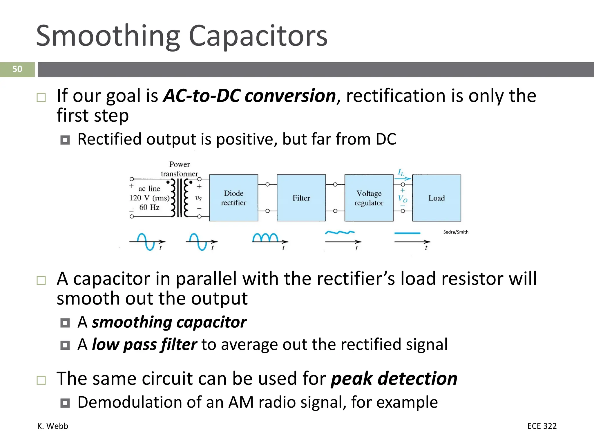
Smoothing Capacitors
If our goal is AC-to-DC conversion, rectification is only the
first step
Rectified output is positive, but far from DC
Sedra/Smith
A capacitor in parallel with the rectifier’s load resistor will
smooth out the output
A smoothing capacitor
A low pass filter to average out the rectified signal
The same circuit can be used for peak detection
Demodulation of an AM radio signal, for example
24.
K. Webb ECE322
51
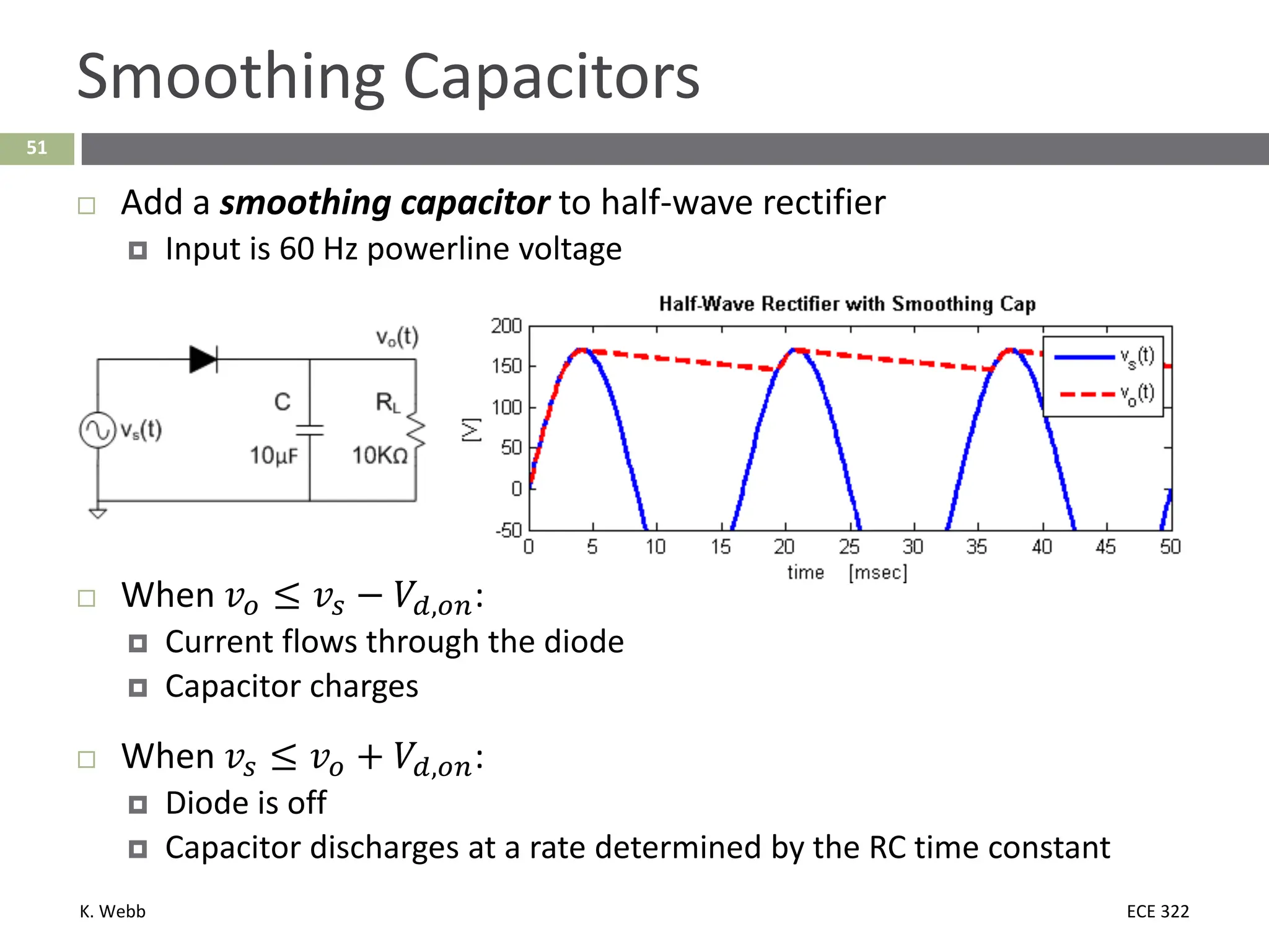
Smoothing Capacitors
Add a smoothing capacitor to half-wave rectifier
Input is 60 Hz powerline voltage
When 𝑣𝑣𝑜𝑜 ≤ 𝑣𝑣𝑠𝑠 − 𝑉𝑉𝑑𝑑,𝑜𝑜𝑜𝑜:
Current flows through the diode
Capacitor charges
When 𝑣𝑣𝑠𝑠 ≤ 𝑣𝑣𝑜𝑜 + 𝑉𝑉𝑑𝑑,𝑜𝑜𝑜𝑜:
Diode is off
Capacitor discharges at a rate determined by the RC time constant
25.
K. Webb ECE322
52
Smoothing Capacitors
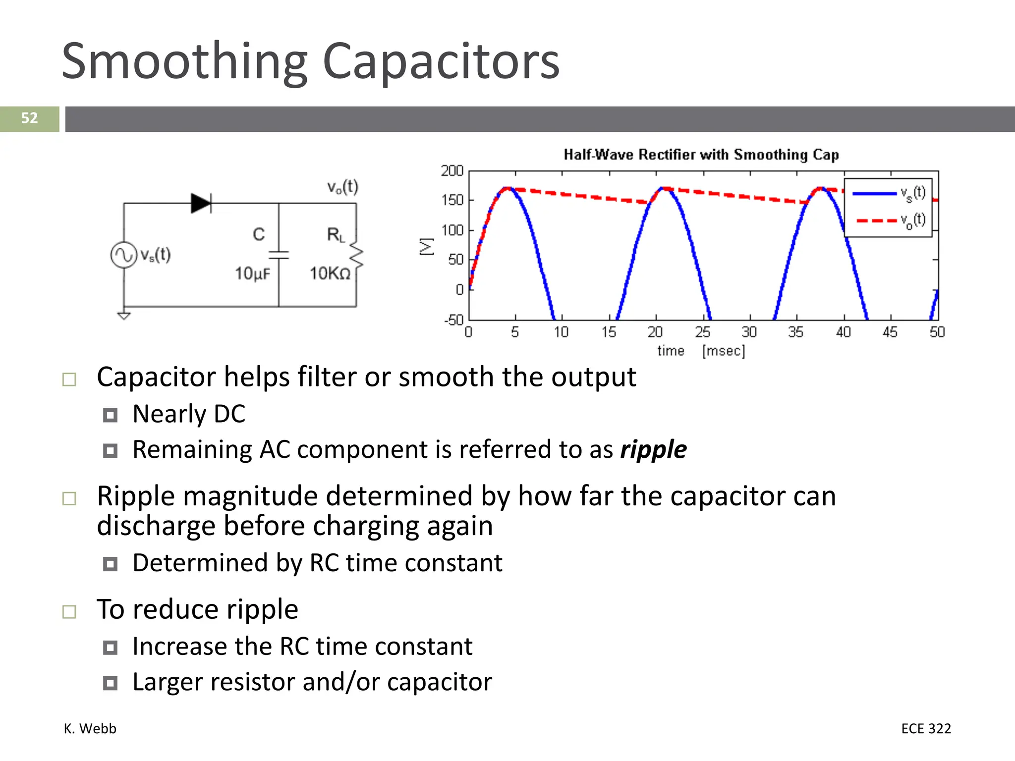
Capacitor helps filter or smooth the output
Nearly DC
Remaining AC component is referred to as ripple
Ripple magnitude determined by how far the capacitor can
discharge before charging again
Determined by RC time constant
To reduce ripple
Increase the RC time constant
Larger resistor and/or capacitor
26.
K. Webb ECE322
53
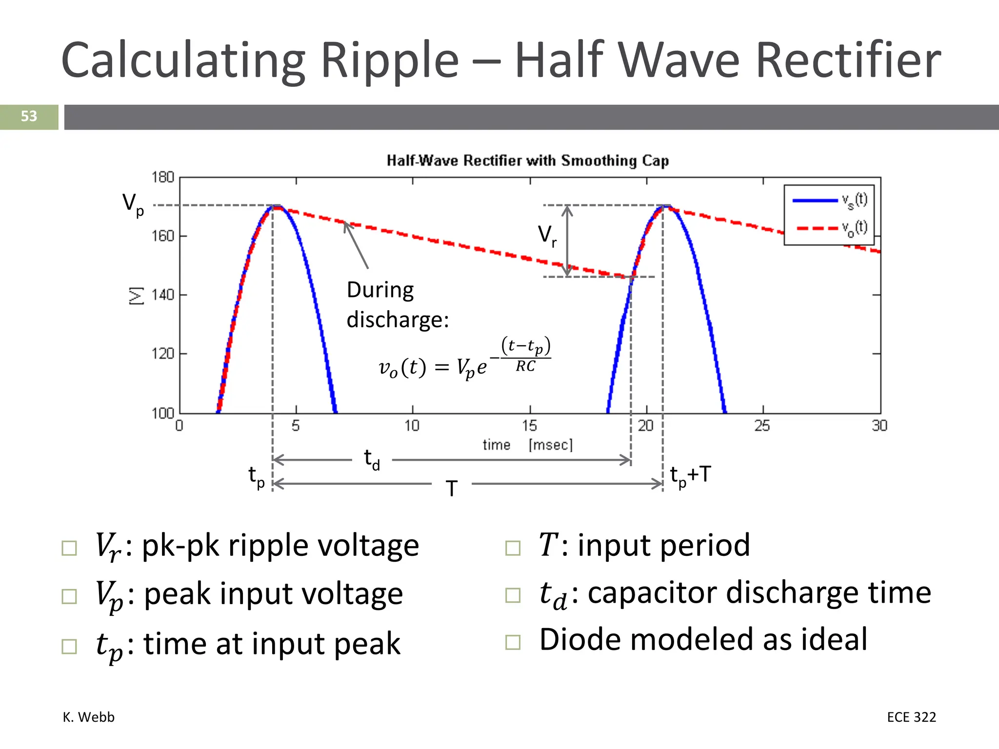
Calculating Ripple – Half Wave Rectifier
𝑉𝑉
𝑟𝑟: pk-pk ripple voltage
𝑉𝑉
𝑝𝑝: peak input voltage
𝑡𝑡𝑝𝑝: time at input peak
𝑘𝑘: input period
𝑡𝑡𝑑𝑑: capacitor discharge time
Diode modeled as ideal
Vr
During
discharge:
𝑣𝑣𝑜𝑜(𝑡𝑡) = 𝑉𝑉
𝑝𝑝𝑒𝑒−
𝑡𝑡−𝑡𝑡𝑝𝑝
𝑅𝑅𝑅𝑅
tp
Vp
tp+T
td
T
27.
K. Webb ECE322
54
Calculating Ripple – Half Wave Rectifier
𝑉𝑉
𝑟𝑟 is the difference between the output voltage at 𝑡𝑡 = 𝑡𝑡𝑝𝑝 and at 𝑡𝑡 = 𝑡𝑡𝑝𝑝 + 𝑡𝑡𝑑𝑑
𝑉𝑉
𝑟𝑟 = 𝑣𝑣𝑜𝑜 𝑡𝑡𝑝𝑝 − 𝑣𝑣𝑜𝑜 𝑡𝑡𝑝𝑝 + 𝑡𝑡𝑑𝑑
where
𝑣𝑣𝑜𝑜 𝑡𝑡𝑝𝑝 = 𝑉𝑉
𝑝𝑝 and 𝑣𝑣𝑜𝑜 𝑡𝑡𝑝𝑝 + 𝑡𝑡𝑑𝑑 = 𝑉𝑉
𝑝𝑝𝑒𝑒−
𝑡𝑡𝑑𝑑
𝑅𝑅𝑅𝑅
so
𝑉𝑉
𝑟𝑟 = 𝑉𝑉
𝑝𝑝 − 𝑉𝑉
𝑝𝑝𝑒𝑒−
𝑡𝑡𝑑𝑑
𝑅𝑅𝑅𝑅 = 𝑉𝑉
𝑝𝑝 1 − 𝑒𝑒−
𝑡𝑡𝑑𝑑
𝑅𝑅𝑅𝑅
Problem is, we do not know 𝑡𝑡𝑑𝑑
Could calculate it, but, instead, assume the following:
𝜏𝜏 = 𝑅𝑅𝐶𝐶 ≫ 𝑘𝑘
From which it follows that
𝑉𝑉
𝑟𝑟 ≪ 𝑉𝑉
𝑝𝑝
𝑡𝑡𝑑𝑑 ≈ 𝑘𝑘
Discharge current is approximately constant:
𝑖𝑖 𝑡𝑡 ≈
𝑉𝑉𝑝𝑝
𝑅𝑅
𝑡𝑡𝑝𝑝 ≤ 𝑡𝑡 ≤ 𝑡𝑡𝑝𝑝 + 𝑡𝑡𝑑𝑑
28.
K. Webb ECE322
55
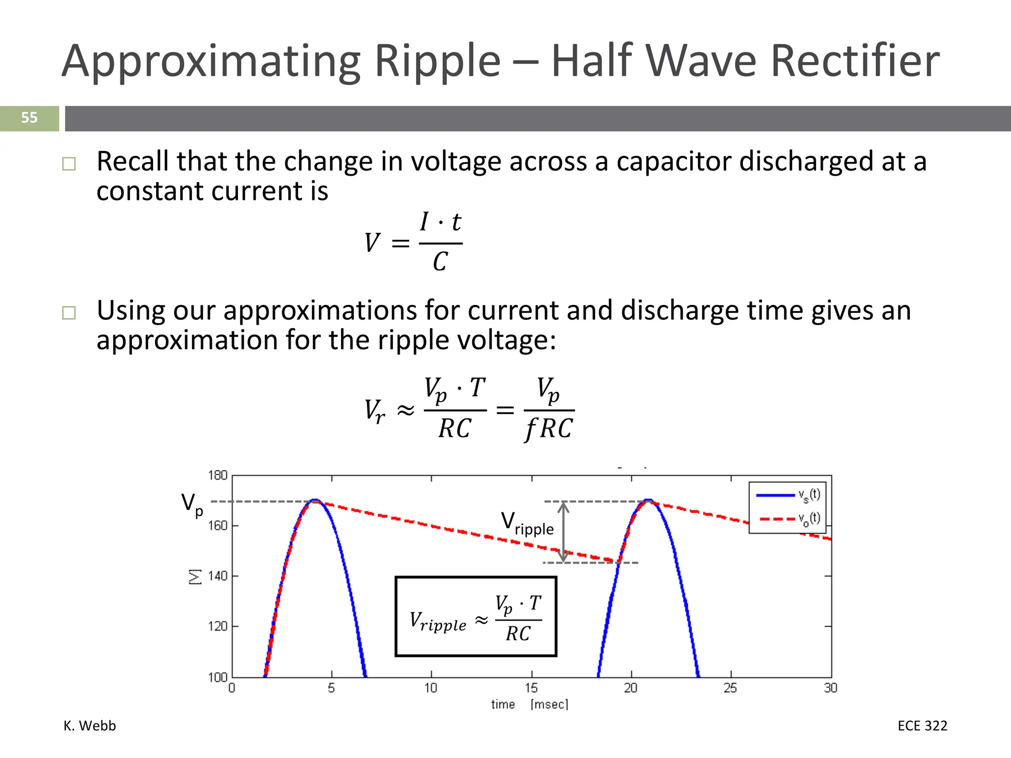
Approximating Ripple – Half Wave Rectifier
Recall that the change in voltage across a capacitor discharged at a
constant current is
𝑉𝑉 =
𝐼𝐼 ⋅ 𝑡𝑡
𝐶𝐶
Using our approximations for current and discharge time gives an
approximation for the ripple voltage:
𝑉𝑉
𝑟𝑟 ≈
𝑉𝑉
𝑝𝑝 ⋅ 𝑘𝑘
𝑅𝑅𝐶𝐶
=
𝑉𝑉
𝑝𝑝
𝑓𝑓𝑅𝑅𝐶𝐶
Vripple
Vp
𝑉𝑉𝑟𝑟𝑟𝑟𝑝𝑝𝑝𝑝𝑟𝑟𝑟𝑟 ≈
𝑉𝑉
𝑝𝑝 ⋅ 𝑘𝑘
𝑅𝑅𝐶𝐶