Download as PDF, PPTX


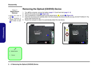

![Schematic Diagrams
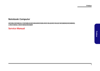
ONTARIO MEM & PCIE I/F, AP
DD R0
DD R1
DD R2
DD R3
DD R4
DD R5
DD R6
DD R7
DD R8
DD R9
DD R1 0
DD R1 1
DD R1 2
DD R1 3
DD R1 4
DD R1 5
M E M _D A T A [ 6 3 : 0 ] 5 , 6
U1 E
M _AD D
0
H1 9
J17
H1 8
H1 7
G1 7
H1 5
G1 8
F1 9
E1 9
T1 9
F1 7
E1 8
W17
E1 6
G1 5
M _D AT A0
O N AR O 2. 0)
T I
(
M _AD D
1
M _AD D
2
PA RT 1 O F 5
M _D AT A1
M _D AT A2
M _AD D
3
M _D AT A3
M _AD D
4
M _D AT A4
M _AD D
5
M _D AT A5
M _AD D
6
M _D AT A6
M _AD D
7
M _AD D
8
M _D AT A7
M _AD D
9
M _D AT A8
M _AD D
10
M _AD D
11
M _D AT A9
M _D ATA 10
M _AD D
12
M _AD D
13
M _D ATA 11
M _D ATA 12
M _AD D
14
M _D ATA 13
M _AD D
15
M _D ATA 14
M _D ATA 15
ME M
ME M
ME M
ME M
ME M
ME M
ME M
ME M
ME M
ME M
ME M
ME M
ME M
ME M
ME M
ME M
_ DQ
_ DQ
_ DQ
_ DQ
_ DQ
_ DQ
_ DQ
_ DQ
_ DQ
_ DQ
_ DQ
_ DQ
_ DQ
_ DQ
_ DQ
_ DQ
S _ H0
S_ L 0
S _ H1
S_ L 1
S _ H2
S_ L 2
S _ H3
S_ L 3
S _ H4
S_ L 4
S _ H5
S_ L 5
S _ H6
S_ L 6
S _ H7
S_ L 7
M
M
M
M
M
M
M
M
EM
EM
EM
EM
EM
EM
EM
EM
_D
_D
_D
_D
_D
_D
_D
_D
M0
M1
M2
M3
M4
M5
M6
M7
D1 5
B1 9
D2 1
H2 2
P2 3
V2 3
AB2 0
AA1 6
A1 6
B1 6
B2 0
A2 0
E2 3
E2 2
J22
J23
R2 2
P2 2
W22
V2 2
A C2 0
A C2 1
AB1 6
A C1 6
M _BA N
K0
M _BA N
K1
M _D ATA 16
M _BA N
K2
M _D ATA 17
M _D ATA 18
M _D 0
M
M _D ATA 19
M _D 1
M
M _D ATA 20
M _D 2
M
M _D 3
M
M _D ATA 21
M _D ATA 22
M _D 4
M
M _D ATA 23
M _D 5
M
M _D 6
M
M _D ATA 24
M _D 7
M
M _D ATA 25
M _D ATA 26
M _D S_H 0
Q
M _D ATA 27
M _D S_L 0
Q
M _D ATA 28
M _D S_H 1
Q
M _D ATA 29
M _D S_L 1
Q
M _D ATA 30
M _D S_H 2
Q
M _D ATA 31
M _D S_L 2
Q
M _D S_H 3
Q
M _D S_L 3
Q
M _D S_H 4
Q
M _D S_L 4
Q
M _D S_H 5
Q
M _D S_L 5
Q
M _D S_H 6
Q
M _D S_L 6
Q
M
M
M
M
M
M
M
M
E M_ C
E M_ C
E M_ C
E M_ C
E M_ C
E M_ C
E M_ C
E M_ C
LK
LK
LK
LK
LK
LK
LK
LK
_H 0
_L 0
_H 1
_L 1
_H 2
_L 2
_H 3
_L 3
5 , 6 M E M_ R E S E T #
5 , 6 M E M_ E V E N T #
M1 7
M1 6
M1 9
M1 8
N1 8
N1 9
L18
L17
M _D ATA 33
M _D ATA 34
M _D ATA 35
M _D ATA 36
M _D ATA 37
M _D ATA 38
M _D ATA 39
M _D S_H 7
Q
M _D S_L 7
Q
L23
N1 7
M _D ATA 40
M _C LK_H 0
M _D ATA 42
M _C LK_L0
M _D ATA 43
M _C LK_H 1
M _D ATA 44
M _C LK_L1
M _C LK_H 2
M _D ATA 45
M _D ATA 46
M _C LK_L2
M _D ATA 47
M _C LK_H 3
M _C LK_L3
M _D ATA 48
M _D ATA 49
M _R SET _L
E
M _D ATA 50
M _EV EN _L
T
M _D ATA 51
M _D ATA 52
M _D ATA 53
5, 6
5, 6
ME M _ C K E 0
ME M _ C K E 1
F1 5
E1 5
M _C E0
K
M _D ATA 54
M _C E1
K
M _D ATA 55
M _D ATA 56
5 D I MM 0 _O D T 0
5 D I MM 0 _O D T 1
6 D I MM 1 _O D T 0
6 D I MM 1 _O D T 1
5 D I MM 0 _C S # 0
5 D I MM 0 _C S # 1
6 D I MM 1 _C S # 0
6 D I MM 1 _C S # 1
5, 6
5, 6
5, 6
ME M _ R A S #
ME M _ C A S #
ME M _ W E #
W19
V1 5
U1 9
W15
T1 7
W16
U1 7
V1 6
U1 8
V1 9
V1 7
ME M
ME M
ME M
ME M
ME M
ME M
ME M
ME M
_ DA T A 0
_ DA T A 1
_ DA T A 2
_ DA T A 3
_ DA T A 4
_ DA T A 5
_ DA T A 6
_ DA T A 7
C
A
B
D
A
B
A
C
18
19
21
20
18
18
21
20
ME M
ME M
ME M
ME M
ME M
ME M
ME M
ME M
_ DA T A 8
_ DA T A 9
_ DA T A 1 0
_ DA T A 1 1
_ DA T A 1 2
_ DA T A 1 3
_ DA T A 1 4
_ DA T A 1 5
C
D
F
F
C
D
F
F
23
23
23
22
22
22
20
21
ME M
ME M
ME M
ME M
ME M
ME M
ME M
ME M
_ DA T A 1 6
_ DA T A 1 7
_ DA T A 1 8
_ DA T A 1 9
_ DA T A 2 0
_ DA T A 2 1
_ DA T A 2 2
_ DA T A 2 3
H
H
K
K
G
H
K
K
21
23
22
21
23
20
20
23
ME M
ME M
ME M
ME M
ME M
ME M
ME M
ME M
_ DA T A 2 4
_ DA T A 2 5
_ DA T A 2 6
_ DA T A 2 7
_ DA T A 2 8
_ DA T A 2 9
_ DA T A 3 0
_ DA T A 3 1
N 23
P 21
T2 0
T2 3
M 20
P 20
R 23
T2 2
ME M
ME M
ME M
ME M
ME M
ME M
ME M
ME M
_ DA T A 3 2
_ DA T A 3 3
_ DA T A 3 4
_ DA T A 3 5
_ DA T A 3 6
_ DA T A 3 7
_ DA T A 3 8
_ DA T A 3 9
V 20
V 21
Y 23
Y 22
T2 1
U 23
W 23
Y 21
ME M
ME M
ME M
ME M
ME M
ME M
ME M
ME M
_ DA T A 4 0
_ DA T A 4 1
_ DA T A 4 2
_ DA T A 4 3
_ DA T A 4 4
_ DA T A 4 5
_ DA T A 4 6
_ DA T A 4 7
Y
A
A
A
A
A
A
Y
20
B2 2
C1 9
A1 8
A2 3
A2 0
B1 9
18
ME M
ME M
ME M
ME M
ME M
ME M
ME M
ME M
_ DA T A 4 8
_ DA T A 4 9
_ DA T A 5 0
_ DA T A 5 1
_ DA T A 5 2
_ DA T A 5 3
_ DA T A 5 4
_ DA T A 5 5
A
Y
A
A
A
A
A
A
C1 7
16
B1 4
C1 4
C1 8
B1 8
B1 5
C1 5
ME M
ME M
ME M
ME M
ME M
ME M
ME M
ME M
_ DA T A 5 6
_ DA T A 5 7
_ DA T A 5 8
_ DA T A 5 9
_ DA T A 6 0
_ DA T A 6 1
_ DA T A 6 2
_ DA T A 6 3
For W250BA Q
U1 A
AA6
Y6
V GA _ R X P 1
V GA _ R X N 1
7
7
VG A_ RXP2
VG A_ RXN 2
7
7
M 0_O D
T0
M _D ATA 57
M _D ATA 58
M 0_O D
T1
M 1_O D
T0
M _D ATA 59
M _D ATA 60
M 1_O D
T1
M _D ATA 61
M 0_C _L0
S
M _D ATA 62
M _D ATA 63
P _G PP_ R 1
XP
P _G PP_ R 1
XN
V GA _ R X P 0
V GA _ R X N 0
7
7
P _G PP_ R 0
XP
P _G PP_ R 0
XN
AB4
A C4
7
7
VG A_ RXP3
VG A_ RXN 3
AA1
AA2
ON _Z V D D
R 2
P_G PP _TX P0
P_G PP _TX N
0
P _G PP_ R 3
XP
Y1 4
AB6
AC6
C1
C2
* 0. 1u _ 1 0 V _ X7 R _ 04
* 0. 1u _ 1 0 V _ X7 R _ 04
V G A _ TX P 0 7
V G A _ TX N 0 7
P_G PP _TX P1
P_G PP _TX N
1
O N TAR I O ( 2. 0)
P ART 2O F 5
P _G PP_ R 2
XP
Y4
Y3
1 VS
M _D ATA 32
M _D ATA 41
5
5
5
5
6
6
6
6
14
15
17
18
14
14
16
16
AB3
AC3
C3
C4
* 0. 1u _ 1 0 V _ X7 R _ 04
* 0. 1u _ 1 0 V _ X7 R _ 04
V G A _ TX P 1 7
V G A _ TX N 1 7
Y1
Y2
C5
C6
* 0. 1u _ 1 0 V _ X7 R _ 04
* 0. 1u _ 1 0 V _ X7 R _ 04
VG A_ TXP2 7
V G A _ T X N2 7
V3
V4
C7
C8
* 0. 1u _ 1 0 V _ X7 R _ 04
* 0. 1u _ 1 0 V _ X7 R _ 04
VG A_ TXP3 7
V G A _ T X N3 7
P_G PP _TX P2
P _G PP_ R 2
XN
P _G PP_ R 3
XN
P_G PP _TX N
2
P_G PP _TX P3
P_G PP _TX N
3
P_ ZVS S
P _ZV D _10
D
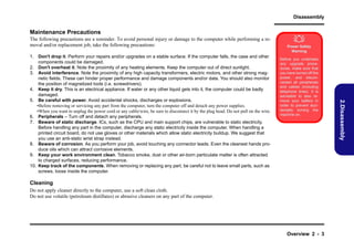
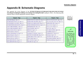
Sheet 2 of 41
ONTARIO MEM &
PCIE I/F, AP
AA1 4
ON _ Z V S S
R 1
B.Schematic Diagrams
5 ,6
5 ,6
5 ,6
5 ,6
5 ,6
5 ,6
5 ,6
5 ,6
5 ,6
5 ,6
5 ,6
5 ,6
5 ,6
5 ,6
5 ,6
5 ,6
R1 8
T1 8
F1 6
M EMO RY I/F
5 , 6 M E M _B A N K 0
5 , 6 M E M _B A N K 1
5 , 6 M E M _B A N K 2
5 , 6 M E M_ D M[ 7 : 0 ]
B
A
A
D
A
C
C
D
PC IE I/F
M EM _
A
M E M _A
M E M _A
M E M _A
M E M _A
M E M _A
M E M _A
M E M _A
M E M _A
M E M _A
M E M _A
M E M _A
M E M _A
M E M _A
M E M _A
M E M _A
1. 27 K _ 1 % _ 0 4
2 K _ 1% _ 0 4
AA1 2
Y1 2
1 5 C _U MI _ P _ R X 1
1 5 C _U MI _ N _ R X 1
P _U I _R P0
M
X
P _U I _R N
M
X 0
P _U I _TX P0
M
P _U I _TX N
M
0
AB1 2
AC1 2
C9
C1 0
0 . 1 u _ 10 V _ X 7 R _ 0 4
0 . 1 u _ 10 V _ X 7 R _ 0 4
C _ U MI _ P _ T X 0 1 5
C _ U MI _ N _ TX 0 1 5
AA1 0
Y1 0
1 5 C _U MI _ P _ R X 0
1 5 C _U MI _ N _ R X 0
P _U I _R P1
M
X
P _U I _R N
M
X 1
P _U I _TX P1
M
P _U I _TX N
M
1
AC1 1
AB1 1
C1 1
C1 2
0 . 1 u _ 10 V _ X 7 R _ 0 4
0 . 1 u _ 10 V _ X 7 R _ 0 4
C _ U MI _ P _ T X 1 1 5
C _ U MI _ N _ TX 1 1 5
AA8
Y8
C1 3
C1 4
0 . 1 u _ 10 V _ X 7 R _ 0 4
0 . 1 u _ 10 V _ X 7 R _ 0 4
C _ U MI _ P _ T X 2 1 5
C _ U MI _ N _ TX 2 1 5
AB8
AC8
C1 5
C1 6
0 . 1 u _ 10 V _ X 7 R _ 0 4
0 . 1 u _ 10 V _ X 7 R _ 0 4
C _ U MI _ P _ T X 3 1 5
C _ U MI _ N _ TX 3 1 5
UM I I/F
5 , 6 M E M_ A D D R [ 1 5 : 0 ]
R 17
ONTARIO MEM & PCIE I/F, AP
AB1 0
A C1 0
1 5 C _U MI _ P _ R X 3
1 5 C _U MI _ N _ R X 3
P _U I _R P2
M
X
P _U I _R N
M
X 2
P _U I _TX N
M
2
A C7
AB7
1 5 C _U MI _ P _ R X 2
1 5 C _U MI _ N _ R X 2
P _U I _R P3
M
X
P _U I _TX P3
M
P _U I _TX P2
M
P _U I _R N
M
X 3
P _U I _TX N
M
3
O N T A R I O_ A P U
ROUTE A- LIN K D IFF PAI R @ 8 5 OHM +/ - 10 %
C8 4 2
C 84 3
C 844
1 0 u_ 6 . 3 V _ X 5 R _ 0 6
0 . 1u _ 1 0 V _ X 7R _ 04
1 0 0 0 p_ 5 0 V _ X 7R _ 0 4
1 .5 V
V T T _M E M
R 67 8
1 K _ 1 % _0 4
Analog Thermal Sensor
3. 3V
M 0_C _L1
S
M 1_C _L0
S
M 1_C _L1
S
M _V R F
E
R 67 9
R 68 0
M 23
* 0 _0 4
0_04
Q1 5
2
1
VC C
OU T
1: ( il 8m s)
2 4m s: il
T H E R M _ V OL T 2 7
1 .5 V
M _R S_L
A
M _C S_L
A
M _WE_L
M _Z VD I O E M _S
D _M
M 2 2 M E M _Z V D D I O
R 6
3 9. 2_ 1 % _ 0 4
R 68 1
1 K _ 1 % _0 4
3
C 3 65
G ND
0 . 1 u _ 10 V _ X 5 R _ 0 4
G 7 11 S T 9 U
C3 6 4
0 . 1u _ 1 0 V _ X 5R _ 0 4
O N TA R I O _A P U
Not e: Open th e sod lermas k for Vi as on Mem int erfac e
R6 c onnec tion to VD DIO_SU S s hould
be direc tly t o the pla n e with ou t a long tr ac e
1
PLACE NEAR U1
3
2
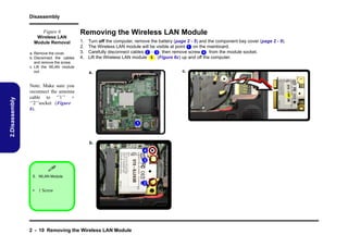
ONTARIO MEM & PCIE I/F, AP B - 3](https://image.slidesharecdn.com/clevow25xbuxw25xbwx-6-7p-w2405-003-131203095714-phpapp02/85/6-7p-w2405-003-51-320.jpg)
![Schematic Diagrams
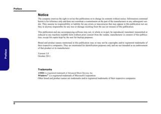
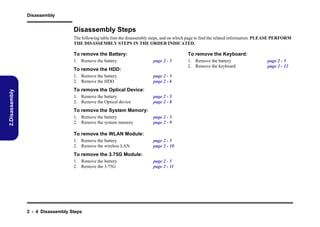
INAGUA DDR3 SO-DIMMS A
SO -D IMM A
INAGUA DDR3 SO-DIMMS A
2,6 M M DD
E _A R[15:0]
B.Schematic Diagrams
6,10,16 S
CLK
0
6,10,16 S T 0
DA A
M _DM
EM
0
M _DM
EM
1
M _DM
EM
2
M _DM
EM
3
M _DM
EM
4
M _DM
EM
5
M _DM
EM
6
M _DM
EM
7
M M QS_
E _D
L0
M M QS_
E _D
L1
M M QS_
E _D
L2
M M QS_
E _D
L3
M M QS_
E _D
L4
M M QS_
E _D
L5
M M QS_
E _D
L6
M M QS_
E _D
L7
D
Q0
D
Q1
D
Q2
D
Q3
D
Q4
D
Q5
D
Q6
D
Q7
D
Q8
D
Q9
D
Q10
D
Q11
D
Q12
D
Q13
D
Q14
D
Q15
D
Q16
D
Q17
D
Q18
D
Q19
D
Q20
D
Q21
D
Q22
D
Q23
D
Q24
D
Q25
D
Q26
D
Q27
D
Q28
D
Q29
D
Q30
D
Q31
D
Q32
D
Q33
D
Q34
D
Q35
D
Q36
D
Q37
D
Q38
D
Q39
D
Q40
D
Q41
D
Q42
D
Q43
D
Q44
D
Q45
D
Q46
D
Q47
D
Q48
D
Q49
D
Q50
D
Q51
D
Q52
D
Q53
D
Q54
D
Q55
D
Q56
D
Q57
D
Q58
D
Q59
D
Q60
D
Q61
D
Q62
D
Q63
BA
0
BA
1
BA
2
S0#
S1#
CK
0
CK
0#
CK
1
CK
1#
CK
E0
CK
E1
CA
S#
RA
S#
WE
#
SA
0
SA
1
SC
L
SD
A
ODT
0
ODT
1
11
28
46
63
136
153
170
187
DM
0
DM
1
DM
2
DM
3
DM
4
DM
5
DM
6
DM
7
12
29
47
64
137
154
171
188
M M QS_
E _D
H0
M M QS_
E _D
H1
M M QS_
E _D
H2
M M QS_
E _D
H3
M M QS_
E _D
H4
M M QS_
E _D
H5
M M QS_
E _D
H6
M M QS_
E _D
H7
2,6
2,6
2,6
2,6
2,6
2,6
2,6
2,6
A0
A1
A2
A3
A4
A5
A6
A7
A8
A9
A10/A
P
A11
A12/B
C#
A13
A14
A15
116
120
2 D M
IM 0_O 0
DT
2 D M
IM 0_O 1
DT
2,6 M _DM
EM
[7:0]
2,6
2,6
2,6
2,6
2,6
2,6
2,6
2,6
98
97
96
95
92
91
90
86
89
85
107
84
83
119
80
78
109
108
79
114
121
101
103
102
104
73
74
115
110
113
197
201
202
200
2,6 M M AN
E _B K0
2,6 M M AN
E _B K1
2,6 M M AN
E _B K2
2 D M
IM 0_C
S#0
2 D M
IM 0_C
S#1
2 M _CLK
EM
_H0
2 M _CLK
EM
_L0
2 M _CLK
EM
_H1
2 M _CLK
EM
_L1
2,6 M M
E _CK 0
E
2,6 M M
E _CK 1
E
2,6 M _CA
EM
S#
2,6 M _RA
EM
S#
2,6 M _WE
EM
#
Sheet 5 of 41
INAGUA DDR3 SODIMMS A
M M AT
E _D A[63:0] 2,6
JDIM 1A
M
M M AD
E _ DR0
M M AD
E _ DR1
M M AD
E _ DR2
M M AD
E _ DR3
M M AD
E _ DR4
M M AD
E _ DR5
M M AD
E _ DR6
M M AD
E _ DR7
M M AD
E _ DR8
M M AD
E _ DR9
M M AD
E _ DR10
M M AD
E _ DR11
M M AD
E _ DR12
M M AD
E _ DR13
M M AD
E _ DR14
M M AD
E _ DR15
DQS
0
DQS
1
DQS
2
DQS
3
DQS
4
DQS
5
DQS
6
DQS
7
10
27
45
62
135
152
169
186
DQS
0#
DQS
1#
DQS
2#
DQS
3#
DQS
4#
DQS
5#
DQS
6#
DQS
7#
5
7
15
17
4
6
16
18
21
23
33
35
22
24
34
36
39
41
51
53
40
42
50
52
57
59
67
69
56
58
68
70
12
9
13
1
14
1
14
3
13
0
13
2
14
0
14
2
14
7
14
9
15
7
15
9
14
6
14
8
15
8
16
0
16
3
16
5
17
5
17
7
16
4
16
6
17
4
17
6
18
1
18
3
19
1
19
3
18
0
18
2
19
2
19
4
M M AT 0
E _D A
M M AT 1
E _D A
M M AT 2
E _D A
M M AT 3
E _D A
M M AT 4
E _D A
M M AT 5
E _D A
M M AT 6
E _D A
M M AT 7
E _D A
M M AT 8
E _D A
M M AT 9
E _D A
M M AT 10
E _D A
M M AT 11
E _D A
M M AT 12
E _D A
M M AT 13
E _D A
M M AT 14
E _D A
M M AT 15
E _D A
M M AT 16
E _D A
M M AT 17
E _D A
M M AT 18
E _D A
M M AT 19
E _D A
M M AT 20
E _D A
M M AT 21
E _D A
M M AT 22
E _D A
M M AT 23
E _D A
M M AT 24
E _D A
M M AT 25
E _D A
M M AT 26
E _D A
M M AT 27
E _D A
M M AT 28
E _D A
M M AT 29
E _D A
M M AT 30
E _D A
M M AT 31
E _D A
M M AT 32
E _D A
M M AT 33
E _D A
M M AT 34
E _D A
M M AT 35
E _D A
M M AT 36
E _D A
M M AT 37
E _D A
M M AT 38
E _D A
M M AT 39
E _D A
M M AT 40
E _D A
M M AT 41
E _D A
M M AT 42
E _D A
M M AT 43
E _D A
M M AT 44
E _D A
M M AT 45
E _D A
M M AT 46
E _D A
M M AT 47
E _D A
M M AT 48
E _D A
M M AT 49
E _D A
M M AT 50
E _D A
M M AT 51
E _D A
M M AT 52
E _D A
M M AT 53
E _D A
M M AT 54
E _D A
M M AT 55
E _D A
M M AT 56
E _D A
M M AT 57
E _D A
M M AT 58
E _D A
M M AT 59
E _D A
M M AT 60
E _D A
M M AT 61
E _D A
M M AT 62
E _D A
M M AT 63
E _D A
J
DIM 1B
M
1.5V
75
76
81
82
87
88
93
94
99
100
105
106
111
112
117
118
123
124
3.3V
S
20m
ils
C9
8
C
99
1u_6.3V 5R_04
_X
0.1u_
16V_Y
5V_
04
VD
D1
VD
D2
VD
D3
VD
D4
VD
D5
VD
D6
VD
D7
VD
D8
VD
D9
VD
D10
VD
D11
VD
D12
VD
D13
VD
D14
VD
D15
VD
D16
VD
D17
VD
D18
199
VD PD
DS
1.5V
R75
77
122
125
1K_0
4
198
30
2,6 M M VE #
E _E NT
2,6 M M
E _RE ET
S #
M RE _DIM 0
V F
M
C100
1
126
C
101
NC1
NC2
NCT S
ET
EV NT
E #
RE T
SE #
VR _DQ
EF
VR _CA
EF
C
102
2
3
8
9
13
14
19
20
25
26
31
32
37
38
43
1u_6.3V 5R_04
_X
1000p_50V 7R_0
_X
4
0.1u_10V 7R_04
_X
VS 1
S
VS 2
S
VS 3
S
VS 4
S
VS 5
S
VS 6
S
VS 7
S
VS 8
S
VS 9
S
VS 10
S
VS 11
S
VS 12
S
VS 13
S
VS 14
S
VS 15
S
44
48
49
54
55
60
61
65
66
71
72
12
7
12
8
13
3
13
4
13
8
13
9
14
4
14
5
15
0
15
1
15
5
15
6
16
1
16
2
16
7
16
8
17
2
17
3
17
8
17
9
18
4
18
5
18
9
19
0
19
5
19
6
VS 16
S
VS 17
S
VS 18
S
VS 19
S
VS 20
S
VS 21
S
VS 22
S
VS 23
S
VS 24
S
VS 25
S
VS 26
S
VS 27
S
VS 28
S
VS 29
S
VS 30
S
VS 31
S
VS 32
S
VS 33
S
VS 34
S
VS 35
S
VS 36
S
VS 37
S
VS 38
S
VS 39
S
VS 40
S
VS 41
S
VS 42
S
VS 43
S
VS 44
S
VS 45
S
VS 46
S
VS 47
S
VS 48
S
VS 49
S
VS 50
S
VS 51
S
VS 52
S
VT E
T _M M
20
3
20
4
VT
T 1
VT
T 2
G
ND1
G
ND2
G1
G2
D
DRR
K-2040 T 4B
1- R
DDRR
K-2040 T
1- R4B
(REV)4.0mm
C LOS E TO S O- DI M M A
1.5V
R
76
1
K_1%
_04
M EF
VR _DIM 0
M
1.5V
R
77
104
+C
C
105
C
106
C
107
C
108
C
109
C
110
C
111
C11
2
1.5V
VT _M
T EM
C
114
C
115
C
116
C
117
C
118
C
119
C
120
C
121
C
122
C
123
0.1u_16V 5V_04
_Y
0.1u_16V 5V_04
_Y
0.1u_16
V_Y
5V_04
0.1u_16
V_Y
5V_04
0.1u_16
V_Y
5V_0
4
0.1u_16V 5V_04
_Y
0.1u_16
V_Y
5V_04
0.1u_16
V_Y
5V_04
0.1u_16
V_Y
5V_04
0.1u_16
V_Y
5V_0
4
B - 6 INAGUA DDR3 SO-DIMMS A
C124
C125
C126
C127
C128
10u_10V
_Y5V
_08
1u_6.3V 5R_04
_X
1u_6.3V 5R_04
_X
1u_6.3V 5R_04
_X
1u_6.3V 5R_04
_X
C103
1
K_1%
_04
C
113
+
*
150u_4V _A *
_B
220u_4V _A 10u_
_V
10V_Y
5V_
08
10u_
10V_Y
5V_
08
1u_6 3V 5R
.
_X _04
1u_6 3V 5R
.
_X _04
10u_
10V_Y
5V_
08
1u_6 3V 5R
.
_X _04
1u_6 3V 5R
.
_X _04
1u_6 3V 5R
.
_X _04
0.1u_10V 5R_04
_X](https://image.slidesharecdn.com/clevow25xbuxw25xbwx-6-7p-w2405-003-131203095714-phpapp02/85/6-7p-w2405-003-54-320.jpg)
![Schematic Diagrams
INAGUA DDR3 SO-DIMMS B
S O-D IMM B
INA GUA DDR3 S O-DIMMS B
2,5 M M DD
E _A R[15:0]
M _DA A[63 0] 2,5
EM
T
:
JD M
IM 2A
2,5 M M AN
E _B K0
2,5 M M AN
E _B K1
2,5 M M AN
E _B K2
2 D M
IM 1_C
S#0
2 D M
IM 1_C
S#1
2 M _CLK
EM
_H2
2 M _CLK
EM
_L2
2 M _CLK
EM
_H3
2 M _CLK
EM
_L3
2,5 M M
E _CK 0
E
2,5 M M
E _CK 1
E
2,5 M _CA
EM
S#
2,5 M _RA
EM
S#
2,5 M _WE
EM
#
R7
8
5,10,16 S
CLK
0
5,10,16 S T 0
DA A
MM M
E _D 0
MM M
E _D 1
MM M
E _D 2
MM M
E _D 3
MM M
E _D 4
MM M
E _D 5
MM M
E _D 6
MM M
E _D 7
O 0
DT
O 1
DT
11
28
46
63
136
153
170
187
D 0
M
D 1
M
D 2
M
D 3
M
D 4
M
D 5
M
D 6
M
D 7
M
12
29
47
64
137
154
171
188
M M QS
E _D _H0
M M QS
E _D _H1
M M QS
E _D _H2
M M QS
E _D _H3
M M QS
E _D _H4
M M QS
E _D _H5
M M QS
E _D _H6
M M QS
E _D _H7
M M QS
E _D _L0
M M QS
E _D _L1
M M QS
E _D _L2
M M QS
E _D _L3
M M QS
E _D _L4
M M QS
E _D _L5
M M QS
E _D _L6
M M QS
E _D _L7
DQ0
DQ1
DQ2
DQ3
DQ4
DQ5
DQ6
DQ7
DQ8
DQ9
D
Q10
D
Q11
D
Q12
D
Q13
D
Q14
D
Q15
D
Q16
D
Q17
D
Q18
D
Q19
D
Q20
D
Q21
D
Q22
D
Q23
D
Q24
D
Q25
D
Q26
D
Q27
D
Q28
D
Q29
D
Q30
D
Q31
D
Q32
D
Q33
D
Q34
D
Q35
D
Q36
D
Q37
D
Q38
D
Q39
D
Q40
D
Q41
D
Q42
D
Q43
D
Q44
D
Q45
D
Q46
D
Q47
D
Q48
D
Q49
D
Q50
D
Q51
D
Q52
D
Q53
D
Q54
D
Q55
D
Q56
D
Q57
D
Q58
D
Q59
D
Q60
D
Q61
D
Q62
D
Q63
B0
A
B1
A
B2
A
S
0#
S
1#
C
K0
C #
K0
C
K1
C #
K1
C 0
KE
C 1
KE
C #
AS
R #
AS
W#
E
S0
A
S1
A
S
CL
S
DA
116
120
2 D M
IM 1_O 0
DT
2 D M
IM 1_O 1
DT
2,5 M M DM
E _
[7:0]
2,5
2,5
2,5
2,5
2,5
2,5
2,5
2,5
A
0
A
1
A
2
A
3
A
4
A
5
A
6
A
7
A
8
A
9
A
10/A
P
A
11
A
12/B
C#
A
13
A
14
A
15
109
108
79
114
121
101
103
102
104
73
74
115
110
113
4.7K
_04 197
201
202
200
3.3V
S
2,5
2,5
2,5
2,5
2,5
2,5
2,5
2,5
98
97
96
95
92
91
90
86
89
85
107
84
83
119
80
78
D 0
QS
D 1
QS
D 2
QS
D 3
QS
D 4
QS
D 5
QS
D 6
QS
D 7
QS
10
27
45
62
135
152
169
186
D 0#
QS
D 1#
QS
D 2#
QS
D 3#
QS
D 4#
QS
D 5#
QS
D 6#
QS
D 7#
QS
5
7
15
17
4
6
16
18
21
23
33
35
22
24
34
36
39
41
51
53
40
42
50
52
57
59
67
69
56
58
68
70
129
131
141
143
130
132
140
142
147
149
157
159
146
148
158
160
163
165
175
177
164
166
174
176
181
183
191
193
180
182
192
194
M _DA A
EM
T 0
M _DA A
EM
T 1
M _DA A
EM
T 2
M _DA A
EM
T 3
M _DA A
EM
T 4
M _DA A
EM
T 5
M _DA A
EM
T 6
M _DA A
EM
T 7
M _DA A
EM
T 8
M _DA A
EM
T 9
M _DA A
EM
T 10
M _DA A
EM
T 11
M _DA A
EM
T 12
M _DA A
EM
T 13
M _DA A
EM
T 14
M _DA A
EM
T 15
M _DA A
EM
T 16
M _DA A
EM
T 17
M _DA A
EM
T 18
M _DA A
EM
T 19
M _DA A
EM
T 20
M _DA A
EM
T 21
M _DA A
EM
T 22
M _DA A
EM
T 23
M _DA A
EM
T 24
M _DA A
EM
T 25
M _DA A
EM
T 26
M _DA A
EM
T 27
M _DA A
EM
T 28
M _DA A
EM
T 29
M _DA A
EM
T 30
M _DA A
EM
T 31
M _DA A
EM
T 32
M _DA A
EM
T 33
M _DA A
EM
T 34
M _DA A
EM
T 35
M _DA A
EM
T 36
M _DA A
EM
T 37
M _DA A
EM
T 38
M _DA A
EM
T 39
M _DA A
EM
T 40
M _DA A
EM
T 41
M _DA A
EM
T 42
M _DA A
EM
T 43
M _DA A
EM
T 44
M _DA A
EM
T 45
M _DA A
EM
T 46
M _DA A
EM
T 47
M _DA A
EM
T 48
M _DA A
EM
T 49
M _DA A
EM
T 50
M _DA A
EM
T 51
M _DA A
EM
T 52
M _DA A
EM
T 53
M _DA A
EM
T 54
M _DA A
EM
T 55
M _DA A
EM
T 56
M _DA A
EM
T 57
M _DA A
EM
T 58
M _DA A
EM
T 59
M _DA A
EM
T 60
M _DA A
EM
T 61
M _DA A
EM
T 62
M _DA A
EM
T 63
J
DIM 2
MB
1.5V
75
76
81
82
87
88
93
94
99
100
105
106
111
112
117
118
123
124
3. 3
VS
20mils
C129
C
130
1u_6.3V 5R_04
_X
0 1u
. _16V
_Y5V
_04
VD
D1
VD
D2
VD
D3
VD
D4
VD
D5
VD
D6
VD
D7
VD
D8
VD
D9
VD
D10
VD
D11
VD
D12
VD
D13
VD
D14
VD
D15
VD
D16
VD
D17
VD
D18
199
VD PD
DS
77
122
125
198
30
2,5 M M VE #
E _E NT
2,5 M M
E _RE ET
S #
1
126
M RE _DIM 1
V F
M
C
131
C132
NC1
NC2
NCT S
ET
EV NT
E #
RE T
SE #
VR _DQ
EF
VR _CA
EF
C133
2
3
8
9
13
14
19
20
25
26
31
32
37
38
43
1u_6.3V 5R_04
_X
1000p_
50V_ 7R_04
X
0.1u_10V 7R
_X _04
VS 1
S
VS 2
S
VS 3
S
VS 4
S
VS 5
S
VS 6
S
VS 7
S
VS 8
S
VS 9
S
VS 10
S
VS 11
S
VS 12
S
VS 13
S
VS 14
S
VS 15
S
44
48
49
54
55
60
61
65
66
71
72
127
128
133
134
138
139
144
145
150
151
155
156
161
162
167
168
172
173
178
179
184
185
189
190
195
196
V S16
S
V S17
S
V S18
S
V S19
S
V S20
S
V S21
S
V S22
S
V S23
S
V S24
S
V S25
S
V S26
S
V S27
S
V S28
S
V S29
S
V S30
S
V S31
S
V S32
S
V S33
S
V S34
S
V S35
S
V S36
S
V S37
S
V S38
S
V S39
S
V S40
S
V S41
S
V S42
S
V S43
S
V S44
S
V S45
S
V S46
S
V S47
S
V S48
S
V S49
S
V S50
S
V S51
S
V S52
S
Sheet 6 of 41
INAGUA DDR3 SODIMMS B
VT _M M
T E
203
204
VT
T1
VT
T2
GN
D1
GN
D2
G1
G2
D
DRR - 20
K 401-T D
P8
D
DRR
K-204
01-T
P8D
(REV)8.0mm
SN:6-86-24204-XXX
C LO SE TO SO - DI MM B
1.5V
R
79
1
K_1%04
_
M RE _DIM 1
V F
M
1.5V
R80
C
136
C
135
C137
C1
38
C
139
C140
C14
1
C
142
C
143
C
134
1K
_1%
_04
C144
0.1u_1
0V_X
5R_04
+
+
*
220u_4
V_V
_A 10u_10V
_Y5
V_08
10
u_10V
_Y5V
_08
1u_6.3V 5R
_X _04
1u_6.3V 5R_04
_X
10u_1
0V_Y _08
5V
1u_6.3V 5R_0
_X
4
1u_
6.3V_X
5R_04
1u_6.3V 5R
_X _04
560u
_2.5V_ 6
6. *6.6* 9
5.
VT _ E
TM M
1.5V
C
145
C
146
C147
C1
48
C
149
C150
C15
1
C
152
C153
C154
0.1u_1
6V_Y _04
5V
0.1u_16V
_Y5V
_04
0.1u
_16V
_Y5V
_04
0.1u_16V 5V_0
_Y
4
0.1u_16V
_Y5V
_04
01
. u_16V
_Y5V
_04
0.1u_16
V_Y
5V_
04
0.1u_16V
_Y5V
_04
0.1u_
16V_
Y5V
_04
0.1u_16V
_Y5
V_04
C155
C
156
C157
C158
C1
59
10u_10V 5V_
_Y
08
1u_6.3V 5R_04
_X
1u_6 3V 5R
.
_X _04
1u_ 3
6. V_XR_04
5
1u_6.3V 5R_
_X
04
INAGUA DDR3 SO-DIMMS B B - 7
B.Schematic Diagrams
M M DDR
E _A
0
M M DDR
E _A
1
M M DDR
E _A
2
M M DDR
E _A
3
M M DDR
E _A
4
M M DDR
E _A
5
M M DDR
E _A
6
M M DDR
E _A
7
M M DDR
E _A
8
M M DDR
E _A
9
M M DDR
E _A
10
M M DDR
E _A
11
M M DDR
E _A
12
M M DDR
E _A
13
M M DDR
E _A
14
M M DDR
E _A
15](https://image.slidesharecdn.com/clevow25xbuxw25xbwx-6-7p-w2405-003-131203095714-phpapp02/85/6-7p-w2405-003-55-320.jpg)
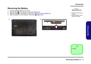
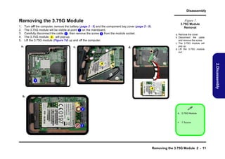
![Schematic Diagrams
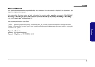
Robson S3 MEM Interface 3/6
COMPONENTS SHOWN ARE EXAMPLES ONLY
AND NOT NECESSARILY QUALIFIED
DDR3 Memory
Interface
U4C
Sheet 9 of 41
Robson S3 MEM
InTERFACE 3/6
14
DQA0_[ 31. .0]
G DDR 5/DD R3
DQA0_ 0
DQA0_ 1
DQA0_ 2
DQA0_ 3
DQA0_ 4
DQA0_ 5
DQA0_ 6
DQA0_ 7
DQA0_ 8
DQA0_ 9
DQA0_ 10
DQA0_ 11
DQA0_ 12
DQA0_ 13
DQA0_ 14
DQA0_ 15
DQA0_ 16
DQA0_ 17
DQA0_ 18
DQA0_ 19
DQA0_ 20
DQA0_ 21
DQA0_ 22
DQA0_ 23
DQA0_ 24
DQA0_ 25
DQA0_ 26
DQA0_ 27
DQA0_ 28
DQA0_ 29
DQA0_ 30
DQA0_ 31
DQA1_ 0
DQA1_ 1
DQA1_ 2
DQA1_ 3
DQA1_ 4
DQA1_ 5
DQA1_ 6
DQA1_ 7
DQA1_ 8
DQA1_ 9
DQA1_10
DQA1_11
DQA1_12
DQA1_13
DQA1_14
DQA1_15
DQA1_16
DQA1_17
DQA1_18
DQA1_19
DQA1_20
DQA1_21
DQA1_22
DQA1_23
DQA1_24
DQA1_25
DQA1_26
DQA1_27
DQA1_28
DQA1_29
DQA1_30
DQA1_31
DQA1_[ 31. .0]
PLACE MVREF DIVIDERS
AND CAPS CLOSE TO ASIC
MV DQ
D
Ra
R12 2
*40. 2_1%_0 4
K 7
2
J2 9
H3 0
H3 2
G2 9
F2 8
F3 2
F3 0
C3 0
F2 7
A 8
2
C2 8
E 7
2
G2 6
D2 6
F2 5
A 5
2
C2 5
E 5
2
D2 4
E 3
2
F2 3
D2 2
F2 1
E 1
2
D2 0
F1 9
A 9
1
D1 8
F1 7
A 7
1
C1 7
E 7
1
D1 6
F1 5
A 5
1
D1 4
F1 3
A 3
1
C1 3
E 1
1
A 1
1
C1 1
F1 1
A9
C9
F9
D8
E7
A7
C7
F7
A5
E5
C3
E1
G7
G6
G1
G3
J6
J1
J3
J5
K 6
2
J2 6
R12 3
MVDDQ
Rb
C204
*100 _04
*0 .1u _10V_X5R_0 4
MV Q
DD
R12 4
R12 5
* 43_1 % 04
2
_
J2 5
K 5
2
* 43_1 % 04
2
_
MAA _0/ MAA 0
0
_
MAA _1/ MAA 1
0
_
MAA _2/ MAA 2
0
_
MAA _3/ MAA 3
0
_
MAA _4/ MAA 4
0
_
MAA _5/ MAA 5
0
_
MA
A0_ 6/MA
A0_ 6
MA
A0_ 7/MA
A0_ 7
MAA _0/ MAA 8
1
_
MAA _1/ MAA 9
1
_
MA
A1_ 2/MA
A_1 0
MA
A1_ 3/MA
A_1 1
MA
A1_ 4/MA
A_1 2
MA
A1_ 5/MAA_13 /BA2
MA
A1_ 6/MAA_14 /BA0
MA
A1_ 7/MAA_15 /BA1
WCKA0_0 /DQMA 0
_
W CK
A0B_0 /DQMA 1
_
WCKA0_1 /DQMA 2
_
W CK
A0B_1 /DQMA 3
_
WCKA1_0 /DQMA 4
_
W CK
A1B_0 /DQMA 5
_
WCKA1_1 /DQMA 6
_
W CK
A1B_1 /DQMA 7
_
EDCA0_ 0/RD QSA 0
_
EDCA0_ 1/RD QSA 1
_
EDCA0_ 2/RD QSA 2
_
EDCA0_ 3/RD QSA 3
_
EDCA1_ 0/RD QSA 4
_
EDCA1_ 1/RD QSA 5
_
EDCA1_ 2/RD QSA 6
_
EDCA1_ 3/RD QSA 7
_
DDBI A 0/WD QSA 0
0_
_
DDBI A 1/WD QSA 1
0_
_
DDBI A 2/WD QSA 2
0_
_
DDBI A 3/WD QSA 3
0_
_
DDBI A 0/WD QSA 4
1_
_
DDBI A 1/WD QSA 5
1_
_
DDBI A 2/WD QSA 6
1_
_
DDBI A 3/WD QSA 7
1_
_
ADB A0/OD TA0
I
ADB A1/OD TA1
I
CLKA0
CLKA0B
CLKA1
CLKA1B
RA
SA0B
RA
SA1B
CA
SA0B
CA
SA1B
CSA B 0
0 _
CSA B 1
0 _
CSA B 0
1 _
CSA B 1
1 _
MVREFDA
MVREFS
A
MEM_ CA RN0
L
MEM_ CA RP0
L
CKEA0
CKEA1
WEA0B
WEA1B
G DDR5 /DD R3
Ra R1 26
DM _ RS
EM
T
*40 .2_1 % 04
_
MA
A0_ 8/MA
A_1 3
M
AA1_8 _RSVD
L1 0
K17
J2 0
H2 3
G2 3
G2 4
H2 4
J1 9
K19
J1 4
K14
J1 1
J1 3
H1 1
G1 1
J1 6
L1 5
E32
E30
A21
C2 1
E13
D1 2
E3
F4
DQM
A0_ 0
DQM
A0_ 1
DQM
A0_ 2
DQM
A0_ 3
DQM
A1_ 0
DQM
A1_ 1
DQM
A1_ 2
DQM
A1_ 3
H2 8
C2 7
A23
E19
E15
D1 0
D6
G5
QSA _0
0
QSA _1
0
QSA _2
0
QSA _3
0
QSA _0
1
QSA _1
1
QSA _2
1
QSA _3
1
H2 7
A27
C2 3
C1 9
C1 5
E9
C5
H4
QSA _0B
0
QSA _1B
0
QSA _2B
0
QSA _3B
0
QSA _0B
1
QSA _1B
1
QSA _2B
1
QSA _3B
1
L1 8
K16
ODTA0
ODTA1
H2 6
H2 5
CLKA0
CLKA0#
G9
H9
CLKA1
CLKA1#
G2 2
G1 7
RAS
A0#
RAS
A1#
G1 9
G1 6
CAS
A0#
CAS
A1#
H2 2
J2 2
CSA b_0
0
G1 3
K13
CSA b_0
1
K20
J1 7
CKE
A0
CKE
A1
G2 5
H1 0
WE
A0#
WE
A1#
G2 0
G1 4
MAA 3
1
MAA _8
1
A_BA2
13 ,14
A_BA0
13 ,14
A_BA1
13 ,14
DQ M
A0_[3 ..0 ] 13
DQMA1_ [3. .0] 1 4
QSA0_[ 3.. 0]
13
QSA _[3 ..0 ]
1
QSA0_0 B
QSA0_1 B
QSA0_2 B
QSA0_3 B
QSA1_0 B
QSA1_1 B
QSA1_2 B
QSA1_3 B
14
13
13
13
13
14
14
14
14
ODTA
0
ODTA
1
13
14
C LKA
0
C LKA #
0
13
13
C LKA
1
C LKA #
1
14
14
RA
SA0#
RA
SA1#
13
14
CA
SA0#
CA
SA1#
13
14
CS
A0b _0
13
CS
A1b _0
14
CKEA
0
CKEA
1
13
14
WEA0#
WEA1#
13
14
MA
A13
13 ,14
T9 7
From GPU
CL K STA
TE
CL K STB
TE
C 205
*ROBSON XT S3
Rb
1 3,14
MAA0
MAA1
MAA2
MAA3
MAA4
MAA5
MAA6
MAA7
MAA8
MAA9
MAA10
MAA11
MAA12
DR A _ RST
M
K8
L7
R1 27
M
AA[12 ..0]
GDD R5/D DR3
DQ A _0/D QA 0
0
_
DQ A _1/D QA 1
0
_
DQ A _2/D QA 2
0
_
DQ A _3/D QA 3
0
_
DQ A _4/D QA 4
0
_
DQ A _5/D QA 5
0
_
DQ A _6/D QA 6
0
_
DQ A _7/D QA 7
0
_
DQ A _8/D QA 8
0
_
DQ A _9/D QA 9
0
_
DQ A _10/ DQA_10
0
DQ A _11/ DQA_11
0
DQ A _12/ DQA_12
0
DQ A _13/ DQA_13
0
DQ A _14/ DQA_14
0
DQ A _15/ DQA_15
0
DQ A _16/ DQA_16
0
DQ A _17/ DQA_17
0
DQ A _18/ DQA_18
0
DQ A _19/ DQA_19
0
DQ A _20/ DQA_20
0
DQ A _21/ DQA_21
0
DQ A _22/ DQA_22
0
DQ A _23/ DQA_23
0
DQ A _24/ DQA_24
0
DQ A _25/ DQA_25
0
DQ A _26/ DQA_26
0
DQ A _27/ DQA_27
0
DQ A _28/ DQA_28
0
DQ A _29/ DQA_29
0
DQ A _30/ DQA_30
0
DQ A _31/ DQA_31
0
DQ A _0/D QA 32
1
_
DQ A _1/D QA 33
1
_
DQ A _2/D QA 34
1
_
DQ A _3/D QA 35
1
_
DQ A _4/D QA 36
1
_
DQ A _5/D QA 37
1
_
DQ A _6/D QA 38
1
_
DQ A _7/D QA 39
1
_
DQ A _8/D QA 40
1
_
DQ A _9/D QA 41
1
_
DQ A _10/ DQA_42
1
DQ A _11/ DQA_43
1
DQ A _12/ DQA_44
1
DQ A _13/ DQA_45
1
DQ A _14/ DQA_46
1
DQ A _15/ DQA_47
1
DQ A _16/ DQA_48
1
DQ A _17/ DQA_49
1
DQ A _18/ DQA_50
1
DQ A _19/ DQA_51
1
DQ A _20/ DQA_52
1
DQ A _21/ DQA_53
1
DQ A _22/ DQA_54
1
DQ A _23/ DQA_55
1
DQ A _24/ DQA_56
1
DQ A _25/ DQA_57
1
DQ A _26/ DQA_58
1
DQ A _27/ DQA_59
1
DQ A _28/ DQA_60
1
DQ A _29/ DQA_61
1
DQ A _30/ DQA_62
1
DQ A _31/ DQA_63
1
MEMORY INTERFACE
B.Schematic Diagrams
13
*0. 1u_ 10V_X R_04
5
*10 0_04
25mm (max)
D M M_RST
E
5
mm (max)
RPD1
*4.99 K 1%_04
_
r oute 50o hms sin gle- ende d/1 00oh ms d iff
a nd k eep sho rt
25mm (ma
x)
RSE 1
R
*10 _04 1 0.0
RSER2
*49. 9_1 % 04
_
M
EM_RST
13, 14
CSHUNT1
*040 2_12 0pF_50 V 5%
_
D ebug onl y, for cloc k ob ser vati on, if n ot need ed, DNI
DD R3/GD DR 3 Me mory Stu ff Optio n
CLKTEST
B
C LKTES
TA
GDDR5
DDR3
MVDDQ
1.5V/1.8V
40.2R
40.2R
Rb
B - 10 Robson S3 MEM Interface 3/6
1.5V
Ra
100R
100R
C2 06
*0.1u _10 V X
_ 5R_ 04
R 128
* 1.1 _1%_04
5
C2 07
R 129
*0. 1u_1 0V_X _04
5R
*51. 1_1 % 4
_0
Place all these components very close to GPU (Within
25mm) and keep all component close to each Other (within
5mm) except Rser2
This basi c topo logy s hould be use d for DRAM_ RST fo r DDR3 /GDDR5 .Thes e
Capa citor s and Resist or val ues ar e an exampl e only . The Series R an d
|| C ap va lues w ill de pend o n the DRAM load a nd wil l have to be
calc ulate d for diffe rent M emory ,DRAM Load and bo ard t o pass Rese t
Sign al Sp ec.](https://image.slidesharecdn.com/clevow25xbuxw25xbwx-6-7p-w2405-003-131203095714-phpapp02/85/6-7p-w2405-003-58-320.jpg)
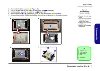
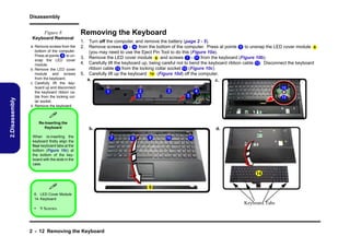
![Schematic Diagrams
Robson S3 Straps 4/6
GPIO21 MUST BE LOW DURING PERSTB WHEN BEING USED TO CONTROL MVDDQ
3.3V _GP
S
U
P IN S T RAP S
W250B AQ
8
GP
IO0
R1
30
*1
0K_0
4
GP IO0
GP
IO1
R1
31
*1
0K_0
4
R1
32
*1
0K_0
4
GP IO1
GP IO2
1
0
R1
33
*1
0K_0
4
R1
34
*1
0K_0
4
R1
35
*1
0K_0
4
R1
36
*1
0K_0
4
R1
37
RE
COM E ED S T ING
M ND
ET
S
1
8
8
GP
IO2
8
GP
IO11
8
GP
IO12
8
GP
IO13
GP IO8
GP IO9
1
0
*1
0K_0
4
GP IO13
0
*1
0K_0
4
*1
0K_0
4
0= DO N
OT INS A RE I S O
T LL
S T R
1 =I N T
S ALL 3 RE IS OR
K
S T
ALLOW FOR PULLUP PADS FOR THES E S TRAPS AND IF THES E GPI OS ARE US ED,
THEY MUS T NOT CONFLICT DURI NG RESET
0
0
GP IO11
GP IO12
R1
39
GP
IO9
8
R1
38
GP
IO8
8
CONFIGU RATION S TR APS-- SEE EAC H DATAB OOK FOR S TR AP DE TAILS
V SY NC_DA C1 1
HSY NC_DA C1 1
S RA S
T P
P
IN
X = D SIGNDE N NT
E
PE DA
NA = N
OT A PLIC LE
P
AB
DE CRIP ION O D A
S
T
F EF ULT S T ING
ET
S
T _P
X WR
S_E B
N
GI O
P 0
P
CIEFU T OU PU SW
LL X
T T
ING
T _DE M H_E
X
E P
N
GI O
P 1
P
CIET NS IT E D
RA M T R E-E P S E B D
M HA IS NA LE
X
X
8,21 V NC_ C1
SY
DA
R1
40
*1
0K_0
4
GP
IO22
GP
IO5
HSY NC_DA C2 0
*1
0K_0
4
*1
0K_0
4
GP IO21
GP IO22
R E ED
ES RV
0
EN ABL E EXTER NA L BIO S R OM
X
1
G
PIO
_22_RO CS
M B
ROM
IDCF
G(2:0)
G [1 1
PIO 3: 1]
VIP
_DE ICE T P
V
_S RA _EN
A
SER IAL
V YN
2S C
RO M TYP E O R MEM O RY AP ER TUR E S IZE S EL EC T
IGN
OREV D ICES RA
IP EV
T PS(Rem
oved on S
eym
our/Whi tler)
s
Sheet 10 of 41
Robson S3 Straps
4/6
XXX
X
RS
VD
*
2.2K
_04
*2.2K
_04
U
6
*0_0
4
*0_0
4
C
209
8
M M
X _SD A R151
AT
7
*
0_04
R E ED
ES RV
0
*
2200p_50V 7R
_X _04
NOTE1: AMD RESERVED C ONF IGURATI ON ST RAPS
2
D+
6
R
153
G NE
E RICC
VD
D
S AT
D A
*
0_04
X
X
1
S LK
C
R
152
0
SEE DA TABO OK FO R DE T IL
A
SEE DA TABO OK FO R DE T IL
A
C
208
3.3V GP
S_ U
*
1000p_ _X
50V 7R_04
M M
X _SC
LK R150
R E ED
ES RV
H YNC
S
V YN
S C
RS
VD
R147
H YNC
2S
AU
D[1]
AU
D[0]
R
146
5
GP DP
U_ LUS
3
A RT
LE
GP DM
U_ INU 8
S
D4
G
ND
T ER
H M
8
R
154
*
0_04
* 3L771A
W8
WG
ALLOW FOR P ULLUP P ADS FOR THESE STRAPS BUT DO NOT I NST ALL RESI STOR. IF THESE GPI OS ARE US ED,
THEY MUS T KEEP "LOW" AND NOT CONFLICT DURI NG RESET .
V _A
GA LER # 27
T
R157
GP
IO21
H2S NC
Y
G ER
EN ICC
G PIO 8
GP
IO2
*
2.2K_0
4
3.3V _GP
S
U
R
155
R156
*
0_04
GP
U_T
ALE T 8 1
R# , 7
3.3VS PU
_G
SMBus gating circuit
*2.2K
_04
3.3V _GP
S
U
7
M M ST
X _R #
R159
*6.8K
_1%
_04
R160
*6.8K
_1%
_04
8
M M DA A
X _S T
R
158
*
0_04
G
27 S D_V A_T E
M
G
H RM
0
GI O
P 21
3.3V _GP
S
U
GPU Thermal Sensor
27 S C_V A_T E
M
G
H RM
0
0
V
GAE BLE
NA
D
BIO
S_R
OM EN
_
0
0
GP IO5
R E ED
ES RV
R E ED
ES RV
GI O
P 9
RS
VD
GE NERICC
1
V SY NC_DA C2 0
*1
0K_0
4
R1
44
GP
IO21
8
R1
43
R1
45
8
8
*1
0K_0
4
R1
42
8 H YNC
S
_DA
C2
*1
0K_0
4
R1
41
GE RIC
NE
C
GI O
P 2
GI O
P 8
BIF GADIS
_V
M M DA A
X _S T
S
G
8
8 V YNC
S
_DA
C2
RS
VD
RS
VD
8
M M CLK
X _S
M M CLK
X _S
S
Q4
D
* T
M N70
02ZH 3
S
S T 0
DA A
5 6,16
,
S
CLK
0
5 6,16
,
Q
5
D
* T 7002Z 3
M N
HS
Robson S3 Straps 4/6 B - 11
B.Schematic Diagrams
8,21 HS C_DA 1
YN
C](https://image.slidesharecdn.com/clevow25xbuxw25xbwx-6-7p-w2405-003-131203095714-phpapp02/85/6-7p-w2405-003-59-320.jpg)
![Schematic Diagrams
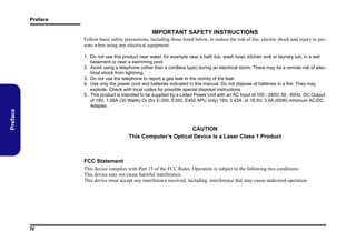
Robson DDR3 MEM CH-A
COMPONENTS SHOWN ARE EXAMPLES ONLY
AND NOT NECESSARILY QUALIFIED
CHANNEL A: 64M X 16 bit X8 DDR3 (RANK0)
U 7
U8
MV D D Q
9
C S A 0b _0
R A S A0 #
C A S A0 #
W EA 0 #
OD T A 0
D QMA 0 _0
D QMA 0 _1
D QMA 0 _2
D QMA 0 _3
QS A 0 _1
QS A 0 _2
QS A 0_ [ 3. . 0 ]
Q SA 0 _0
Q SA 0 _1
Q SA 0 _2
Q SA 0 _3
K1
L2
J3
K3
L3
F3
C7
QS A 0_ 0 B
QS A 0_ 1 B
QS A 0_ 2 B
QS A 0_ 3 B
QS A0 _ 0B
QS A0 _ 1B
QS A0 _ 2B
QS A0 _ 3B
E7
D3
QS A 0 _1 B
QS A 0 _2 B
9
9
9
9
D Q MA 0_ 1
D Q MA 0_ 2
G3
B7
T2
9, 1 4 ME M_ R S T
L8
OD T
CS
RAS
CAS
WE
D QS L
D QS U
D ML
D MU
D QS L
D QS U
RESE T
ZQ
V D D Q# A1
V D D Q# A8
V D D Q#C 1
V D D Q#C 9
V D D Q#D 2
V D D Q# E9
V D D Q# F1
V D D Q#H 2
V D D Q#H 9
V S S # A9
V S S # B3
V S S # E1
V S S #G8
V SS # J2
V SS # J8
V S S #M1
V S S #M9
V S S # P1
V S S # P9
V SS # T1
V SS # T9
MV D D Q
A1
A8
C1
C9
D2
E9
F1
H2
H9
A9
B3
E1
G8
J2
J8
M1
M9
P1
P9
T1
T9
9
9
9
C LK A 0
C LK A 0#
C KE A 0
OD T A 0
9
9
9
9
C S A 0 b_ 0
R AS A 0 #
C AS A 0 #
W E A 0#
J7
K7
K9
K1
L2
J3
K3
L3
QS A 0_ 3
QS A 0_ 0
F3
C7
D QMA 0 _3
D QMA 0 _0
E7
D3
QS A 0 _3 B
QS A 0_ 0B
G3
B7
T2
9, 1 4 ME M_R ST
L8
CK
CK
CKE
OD T
CS
RAS
CAS
WE
D QS L
D QS U
D ML
D MU
D QS L
D QS U
RESE T
ZQ
V D D Q#A 1
V D D Q#A 8
V D D Q #C 1
V D D Q #C 9
V D D Q #D 2
V D D Q#E 9
V D D Q#F 1
V D D Q #H 2
V D D Q #H 9
V S S #A 9
V S S #B 3
V S S #E 1
V S S #G8
VS S # J2
VS S # J8
V S S #M1
V S S #M9
V S S #P 1
V S S #P 9
VS S # T1
VS S # T9
C 34 1
C 3 42
* 0. 1 u_ 10 V _X 5 R _0 4
C 3 40
*0 . 1u _1 0V _ X 5R _ 04
C 35 4
C 3 55
C 35 6
C 3 57
C 35 8
C 3 59
C 36 0
C 3 61
C 36 2
C 3 63
C 37 5
B2
D9
G7
K2
K8
N1
N9
R1
R9
C 3 76
C 37 7
C 3 78
MV D D Q
M VD D Q
A1
A8
C1
C9
D2
E9
F1
H2
H9
A9
B3
E1
G8
J2
J8
M1
M9
P1
P9
T1
T9
C 33 9
MV D D Q
M VD D Q
VD D #B 2
V D D #D 9
V D D #G7
VD D #K 2
VD D #K 8
V D D #N 1
V D D #N 9
V D D #R 1
V D D #R 9
C 3 38
* 0. 1 u_ 10 V _X 5 R _0 4
9
C 33 7
*0 . u _1 0V _ X 5R _ 04
1
D QA 0 _[ 7 . 0 ]
.
C 3 36
*0 . 1 u_ 10 V _X 5 R _0 4
A0 _ 3
A0 _ 2
A0 _ 5
A0 _ 0
A0 _ 7
A0 _ 4
A0 _ 6
A0 _ 1
C 33 5
*1 u_ 6. 3 V _X 5R _0 4
DQ
DQ
DQ
DQ
DQ
DQ
DQ
DQ
C 3 34
*1 u _6 . 3V _ X5 R _ 04
D7
C3
C8
C2
A7
A2
B8
A3
C 33 3
*1u _ 6. 3 V_ X 5R _0 4
D QA 0_ [ 31 . . 24 ] 9
*1 u _6 . 3V _ X5 R _ 04
A0 _ 27
A0 _ 28
A0 _ 25
A0 _ 31
A0 _ 29
A0 _ 30
A0 _ 24
A0 _ 26
* 0. 1 u_ 10 V _X 5 R _0 4
B A0
B A1
B A2
DQ
DQ
DQ
DQ
DQ
DQ
DQ
DQ
*0 . 1u _1 0V _ X 5R _ 04
M2
N8
M3
D QU 0
D QU 1
D QU 2
D QU 3
D QU 4
D QU 5
D QU 6
D QU 7
E3
F7
F2
F8
H3
H8
G2
H7
* 0. 1 u_ 10 V _X 5 R _0 4
A_ BA0
A_ BA1
A_ BA2
QL0
QL1
QL2
QL3
QL4
QL5
QL6
QL7
*0 . u _1 0V _ X 5R _ 04
1
9, 1 4
9, 1 4
9, 1 4
A0
A1
A2
A3
A4
A5
A6
A7
A8
A9
A 10 / A P
A 11
A 12 / B C
A 13
A 14
A 15
D
D
D
D
D
D
D
D
*0 . 1 u_ 10 V _X 5 R _0 4
MV D D Q
V RE F CA
V RE F DQ
*1 u_ 6. 3 V _X 5R _0 4
B2
D9
G7
K2
K8
N1
N9
R1
R9
D QA 0 _[ 2 3. . 1 6] 9
N3
P7
P3
N2
P8
P2
R8
R2
T8
R3
L7
R7
N7
T3
T7
M7
*1 u _6 . 3V _ X5 R _ 04
9
9
9
9
D QMA 0_ [ 3. . 0 ]
CK
CK
CKE
V D D # B2
VD D #D 9
VD D #G7
V D D # K2
V D D # K8
VD D #N 1
VD D #N 9
VD D #R 1
VD D #R 9
MA A 0
MA A 1
MA A 2
MA A 3
MA A 4
MA A 5
MA A 6
MA A 7
MA A 8
MA A 9
MA A 1 0
MA A 1 1
MA A 1 2
MA A 13
M8
H1
*1u _ 6. 3 V_ X 5R _0 4
9
C LK A 0
C LK A 0 #
C K E A0
J7
K7
K9
BA0
BA1
BA2
QA 0_ 23
QA 0_ 22
QA 0_ 18
QA 0_ 21
QA 0_ 16
QA 0_ 19
QA 0_ 17
QA 0_ 20
V R E FC _U 8
V R E FD _U 8
*1 0 u_ 6. 3 V _X 5 R _0 6
9
9
9
M2
N8
M3
D
D
D
D
D
D
D
D
9
*10 u _6 . 3V _ X5 R _ 06
A_ B A 0
A_ B A 1
A_ B A 2
D7
C3
C8
C2
A7
A2
B8
A3
D QA 0 _[ 1 5. . 8 ]
*1 u _6 . 3V _ X5 R _ 04
9, 4
1
9, 4
1
9, 4
1
D QU 0
D QU 1
D QU 2
D QU 3
D QU 4
D QU 5
D QU 6
D QU 7
D QA 0_ 11
D QA 0_ 9
D QA 0_ 8
D QA 0_ 10
D QA 0_ 15
D QA 0_ 12
D QA 0_ 14
D QA 0_ 13
E3
F7
F2
F8
H3
H8
G2
H7
*1 0 u_ 6. 3 V _X 5R _0 6
Sheet 13 of 41
Robson DDR3 MEM
CH-A
A0
A1
A2
A3
A4
A5
A6
A7
A8
A9
A 10 / A P
A 11
A 12 / B C
A 13
A 14
A 15
D QL0
D QL1
D QL2
D QL3
D QL4
D QL5
D QL6
D QL7
*1u _ 6. 3 V_ X 5R _0 4
MA A 0
MA A 1
MA A 2
MA A 3
MA A 4
MA A 5
MA A 6
MA A 7
MA A 8
MA A 9
M AA 1 0
M AA 1 1
M AA 1 2
MA A 13
N3
P7
P3
N2
P8
P2
R8
R2
T8
R3
L7
R7
N7
T3
T7
M7
V RE F CA
V RE F DQ
*1u _ 6. 3 V_ X 5R _0 4
MA A 0
MA A 1
MA A 2
MA A 3
MA A 4
MA A 5
MA A 6
MA A 7
MA A 8
MA A 9
MA A1 0
MA A1 1
MA A1 2
MA A 1 3
9, 1 4 MA A [ 1 3. . 0 ]
M8
H1
*10 u _6 . 3V _ X5 R _ 06
B.Schematic Diagrams
V R E F C _U 7
V R E F D _U 7
M VD D Q
MV D D Q
R 1 69
*4 . 99 K _1 %_ 04
R1 7 0
* 4. 9 9K _ 1% _0 4
V RE F C_ U8
V R E F C _U 7
R 1 65
9
OD T A0
*24 3_ 1 %_ 04
OD T A0
J1
L1
J9
L9
V S S Q# B1
V S S Q# B9
V S S Q#D 1
V S S Q#D 8
V S S Q# E2
V S S Q# E8
V S S Q# F9
V S S Q#G1
V S S Q#G9
N C # J1
N C # L1
N C # J9
N C # L9
10 0-B A LL
SD R A M D D R 3
* K 4W 1G 16 46 G-B C 11
B1
B9
D1
D8
E2
E8
F9
G1
G9
R 1 66
* 24 3_ 1% _0 4
J1
L1
J9
L9
V S S Q#B 1
V S S Q#B 9
V SS Q #D 1
V SS Q #D 8
V S S Q#E 2
V S S Q#E 8
V S S Q#F 9
V SS Q #G1
V SS Q #G9
N C # J1
N C # L1
N C # J9
N C # L9
1 0 0-B A LL
S D R AM D D R 3
B1
B9
D1
D8
E2
E8
F9
G1
G9
R1 7 4
C 32 5
* 0. 1 u_ 10 V _X 5R _0 4
*4 . 99 K _1 %_ 04
R 1 73
C 3 26
*0 . 1u _1 0V _ X5 R _ 04
* 4. 9 9K _ 1% _0 4
M VD D Q
MV D D Q
* K4 W 1G1 6 46 G-B C 11
R 1 77
*4 . 99 K _1 %_ 04
R1 7 8
* 4. 9 9K _ 1% _0 4
V RE F D_ U8
V R E F D _U 7
C 3 30
*0 . 1u _1 0V _ X5 R _ 04
* 4. 9 9K _ 1% _0 4
R1 8 2
R 1 81
C 32 9
* 0. 1 u_ 10 V _X 5R _0 4
*4 . 99 K _1 %_ 04
9
C L KA 0
R 18 5
*5 6_ 04
R 18 6
*5 6_ 04
9
C L KA 0 #
B - 14 Robson DDR3 MEM CH-A
*0 . 0 1u _1 6V _ X7 R _ 04
C3 5 3](https://image.slidesharecdn.com/clevow25xbuxw25xbwx-6-7p-w2405-003-131203095714-phpapp02/85/6-7p-w2405-003-62-320.jpg)
![Schematic Diagrams
Robson DDR3 MEM CH-B
C OMPONEN TS SHOWN AR E EXA MPLES ON LY
A ND N OT NE CE SSA RILY QUA LIFIED
QS A 1_ 0B
QS A 1_ 1B
QS A 1_ 2B
QS A 1_ 3B
C S A 1b _0
R A S A1 #
C A S A1 #
W EA 1 #
QS A 1_ 0B
QS A 1_ 1B
QS A 1_ 2B
QS A 1_ 3B
QS A 1 _0
QS A 1 _1
F3
C7
E7
D3
G3
B7
D QA 1 _2 1
D QA 1 _2 2
D QA 1 _1 6
D QA 1 _2 3
D QA 1 _1 8
D QA 1 _2 0
D QA 1 _1 9
D QA 1 _1 7
D 7
C 3
C 8
C 2
A7
A2
B8
A3
D QA 1 _2 8
D QA 1 _2 6
D QA 1 _3 1
D QA 1 _2 4
D QA 1 _2 9
D QA 1 _2 5
D QA 1 _3 0
D QA 1 _2 7
D QA 1 _[ 2 3. . 16 ] 9
MV D D Q
C 3 95
C 3 96
C 39 7
C 39 8
C 3 99
C 4 00
*0 . 1u _1 0V _ X 5R _ 04
C 3 94
*0 . 1u _1 0V _ X5 R _ 04
C 39 3
*0. 1 u_ 10 V _X 5 R _0 4
C 39 2
*0. 1 u_ 10 V _X 5R _0 4
C3 9 1
* 0. 1 u_ 10 V_ X 5R _ 04
MV D D Q
D QA 1 _[ 3 1. . 24 ] 9
*1 u_ 6. 3 V _X 5 R _0 4
D QU 0
D QU 1
D QU 2
D QU 3
D QU 4
D QU 5
D QU 6
D QU 7
E3
F7
F2
F8
H 3
H 8
G 2
H 7
*1 u_ 6. 3 V _X 5R _ 0 4
QL0
QL1
QL2
QL3
QL4
QL5
QL6
QL7
O DT
C S
R AS
C AS
WE
D QS L
D QS U
D ML
D MU
D QS L
D QS U
R ES E T
L8
R 23 6
*56 _0 4
C 41 1
*0 . 1u _ 16 V_ X7 R _ 04
0
J1
L1
J9
L9
N C #J 1
N C #L 1
N C #J 9
N C #L 9
V D D Q# A1
V D D Q# A8
VD D Q#C 1
VD D Q#C 9
VD D Q#D 2
V D D Q# E9
V D D Q# F1
VD D Q#H 2
VD D Q#H 9
VS S # A9
VS S # B3
VS S # E1
V S S #G8
V SS # J2
V SS # J8
V S S #M1
V S S #M9
VS S # P1
VS S # P9
V SS # T1
V SS # T9
V S S Q# B1
V S S Q# B9
V S S Q#D 1
V S S Q#D 8
V S S Q# E2
V S S Q# E8
V S S Q# F9
V S S Q#G1
V S S Q#G9
1 00 -BA L L
S DRA M DDR3
*K 4 W1 G16 4 6G-B C 1 1
A9
B3
E1
G8
J2
J8
M1
M9
P1
P9
T1
T9
C LK A 1
C LK A 1 #
C K EA 1
OD T A 1
9
9
9
9
C S A1 b_ 0
R A SA 1 #
C A SA 1 #
WE A 1 #
J7
K7
K9
K1
L2
J3
K3
L3
QS A 1_ 2
QS A 1_ 3
F3
C7
D QMA 1 _2
D QMA 1 _3
E7
D3
QS A 1_ 2B
QS A 1_ 3B
G3
B7
BA0
BA1
BA2
C K
C K
C KE
O DT
C S
R AS
C AS
WE
D QSL
D QSU
D ML
D MU
D QSL
D QSU
T2
9 , 13 ME M_ R S T
R ES E T
L8
ZQ
B1
B9
D1
D8
E2
E8
F9
G1
G9
R 20 6
*24 3_ 1% _0 4
J1
L1
J9
L9
N C #J 1
N C #L 1
N C #J 9
N C #L 9
V D D #B 2
VD D #D 9
VD D #G7
V D D #K 2
V D D #K 8
VD D #N 1
VD D #N 9
VD D #R 1
VD D #R 9
V D D Q#A 1
V D D Q#A 8
V D D Q #C 1
V D D Q #C 9
V D D Q #D 2
V D D Q#E 9
V D D Q#F 1
V D D Q #H 2
V D D Q #H 9
V S S #A 9
V S S #B 3
V S S #E 1
V S S #G8
V SS # J2
V SS # J8
V S S #M1
V S S #M9
V S S #P 1
V S S #P 9
V SS # T1
V SS # T9
V S S Q#B 1
V S S Q#B 9
V S SQ #D 1
V S SQ #D 8
V S S Q#E 2
V S S Q#E 8
V S S Q#F 9
V S SQ #G1
V S SQ #G9
B2
D 9
G 7
K2
K8
N 1
N 9
R 1
R 9
C4 1 2
C 41 3
C 41 4
C 4 15
C 4 16
C 4 17
C 41 8
C 41 9
C 4 20
MV D D Q
A1
A8
C 1
C 9
D 2
E9
F1
H 2
H 9
C 4 21
A9
B3
E1
G 8
J2
J8
M1
M9
P1
P9
T1
T9
B1
B9
D 1
D 8
E2
E8
F9
G 1
G 9
C 43 5
C 43 6
C 4 37
MV D D Q
C4 3 4
Sheet 14 of 41
Robson DDR3 MEM
CH-B
*0 . 1u _1 0V _ X 5R _ 04
9
9
9
M2
N8
M3
*0 . 1u _1 0V _ X5 R _ 04
MV D D Q
A1
A8
C1
C9
D2
E9
F1
H2
H9
A _B A 0
A _B A 1
A _B A 2
*0. 1 u_ 10 V _X 5 R _0 4
9 , 13
9 , 13
9 , 13
*0. 1 u_ 10 V _X 5R _0 4
B2
D9
G7
K2
K8
N1
N9
R1
R9
* 0. 1 u_ 10 V_ X 5R _ 04
V D D # B2
VD D #D 9
VD D #G7
V D D # K2
V D D # K8
VD D #N 1
VD D #N 9
VD D #R 1
VD D #R 9
*1 u_ 6. 3 V _X 5 R _0 4
C K
C K
C KE
T2
9 , 13 ME M_ R S T
OD T A 1
R 23 7
*56 _0 4
D
D
D
D
D
D
D
D
*1 u_ 6. 3 V _X 5R _ 0 4
9
9
9
9
K1
L2
J3
K3
L3
C LK A 1
C LK A 1#
A0
A1
A2
A3
A4
A5
A6
A7
A8
A9
A 1 0/ A P
A1 1
A 1 2/ B C
A1 3
A1 4
A1 5
*1 u_ 6. 3V _ X 5R _ 04
C LK A 1
C LK A 1 #
C K E A1
OD T A 1
J7
K7
K9
BA0
BA1
BA2
ZQ
9
MV D D Q
V RE F CA
V RE F DQ
*1u _6 . 3V _ X5 R _ 04
9
9
9
QS A 1_ 0
QS A 1_ 1
QS A 1_ 2
QS A 1_ 3
M2
N8
M3
R 20 5
*24 3_ 1% _0 4
9
9
N3
P7
P3
N2
P8
P2
R8
R2
T8
R3
L7
R7
N7
T3
T7
M7
* 1u _6 . 3V _X 5 R _0 4
D QMA 1 _0
D QMA 1 _1
D QMA 1 _2
D QMA 1 _3
A _B A 0
A _B A 1
A _B A 2
QS A 1 _0 B
QS A 1 _1 B
O D TA 1
D QA 1 _[ 7 . . ]
0
MA A 0
MA A 1
MA A 2
MA A 3
MA A 4
MA A 5
MA A 6
MA A 7
MA A 8
MA A 9
MA A1 0
MA A1 1
MA A1 2
MA A 13
MV D D Q
9 , 13
9 , 13
9 , 13
D Q MA 1_ 0
D Q MA1 _ 1
9
QA1 _ 11
QA1 _ 12
QA1 _ 9
QA1 _ 8
QA1 _ 14
QA1 _ 15
QA1 _ 10
QA1 _ 13
V R E F C _U 12 M8
V R E F D _U 12 H 1
MV D D Q
+C 83
*1 0u _6 . 3V _ X5 R _ 06
9
9
9
9
D
D
D
D
D
D
D
D
9
*1 0u _6 . V _X 5 R _0 6
3
QS A1 _ 3 . . 0]
[
D7
C3
C8
C2
A7
A2
B8
A3
D QA 1 _[ 1 5. . 8]
*10 u_ 6. 3 V _X 5 R _0 6
9
D QA 1 _0
D QA 1 _2
D QA 1 _7
D QA1 _ 3
D QA 1 _6
D QA 1 _4
D QA 1 _5
D QA1 _ 1
* 10 u_ 6. 3 V_ X 5R _ 06
9 D Q MA1 _ [ . . 0]
3
D QU 0
D QU 1
D QU 2
D QU 3
D QU 4
D QU 5
D QU 6
D QU 7
E3
F7
F2
F8
H3
H8
G2
H7
*1 u_ 6. 3V _ X 5R _ 04
MA A 0
MA A 1
MA A 2
MA A 3
MA A 4
MA A 5
MA A 6
MA A 7
MA A 8
MA A 9
MA A1 0
MA A1 1
MA A1 2
MA A 13
A0
A1
A2
A3
A4
A5
A6
A7
A8
A9
A 1 0/ A P
A1 1
A 1 2/ B C
A1 3
A1 4
A1 5
D QL0
D QL1
D QL2
D QL3
D QL4
D QL5
D QL6
D QL7
*1u _6 . 3V _ X5 R _ 04
9 , 3 MA A [ 1 3. . 0]
1
N3
P7
P3
N2
P8
P2
R8
R2
T8
R3
L7
R7
N7
T3
T7
M7
U1 2
V RE F CA
V RE F DQ
MV D D Q
8
* 22 0u _4 V _V _A
MV D D Q
R 22 4
*4. 9 9K _ 1% _0 4
R 2 25
* 4. 99 K _1 %_ 04
V R E F C _ U 11
R 23 2
C 3 87
*0 . 1u _1 0V _ X5 R _0 4
*4. 9 9K _ 1% _0 4
V R E F D _U 1 1
R 2 33
C 38 8
*0. 1 u_ 10 V _X 5R _ 04
* 4. 99 K _1 %_ 04
10 0 - A L L
B
S DRA M DDR3
*K 4W 1 G16 46 G-B C 11
MV D D Q
MV D D Q
R 22 6
*4 . 9 K_ 1% _0 4
9
VR EF C _ U 12
R2 2 7
* 4. 9 9K _1 %_ 04
V R E F D _U 1 2
C 3 89
C 39 0
R2 3 5
*0 . 1u _1 0V _ X5 R _0 4
*0. 1 u_ 10 V _X 5R _ 04
*4 . 9 K_ 1% _0 4
9
* 4. 9 9K _1 %_ 04
R 23 4
Robson DDR3 MEM CH-B B - 15
B.Schematic Diagrams
MA A 0
MA A 1
MA A 2
MA A 3
MA A 4
MA A 5
MA A 6
MA A 7
MA A 8
MA A 9
MA A1 0
MA A1 1
MA A1 2
MA A 1 3
M8
H1
* 1u _6 . 3V _X 5 R _0 4
U1 1
V R E F C _U 11
V R E F D _U 11
CHANNEL A: 64M X 16 bit X8 DDR3 (RANK1)](https://image.slidesharecdn.com/clevow25xbuxw25xbwx-6-7p-w2405-003-131203095714-phpapp02/85/6-7p-w2405-003-63-320.jpg)
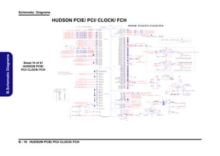
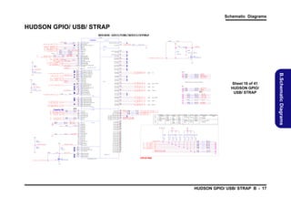
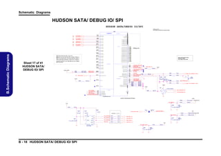
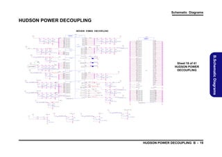
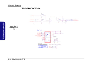
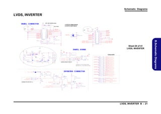
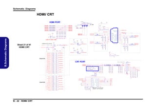
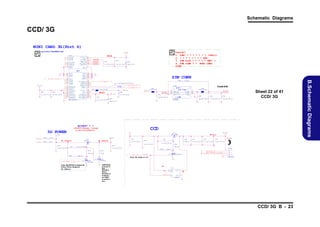
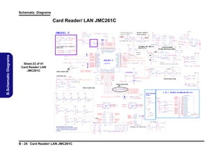
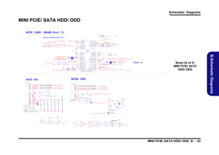
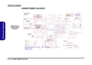
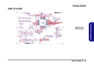
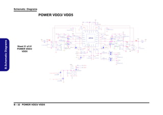
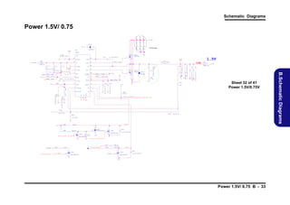
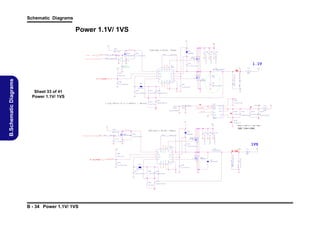
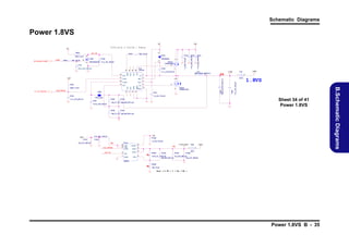

This document provides service instructions for notebook computer models W255BU, W258BUQ-C, W258BUQ, W252BUM, W255BU, W251BUQ, W251BUQC, W258BWQ, W258BWQ-C, W251BWQ-C, W251BWQ, and W255BW. It contains safety and handling instructions, disassembly instructions, part lists, schematic diagrams, and instructions for updating the BIOS firmware. The document is intended for use by service personnel to maintain and repair these notebook computer models.


