This document provides an overview of nanotechnology, including its definition, applications, market prospects, investments, and risks. Some key points:
- Nanotechnology involves manipulating materials at the nanoscale (1-100 nanometers) where their properties differ from larger scales due to greater surface area and quantum effects. It has diverse applications in materials, electronics, medicine, and more.
- The nanotechnology market is growing rapidly, expected to reach 15% of global manufacturing by 2014. Investments in nanotech companies have reached over $1 billion. It will be a major technological force shaping many industries.
- While offering opportunities, nanoparticles may pose new health and environmental risks that are not yet fully understood. More research


![than current devices, to simulate a fuller range of
sounds. The implant is connected to a small
microprocessor and a microphone in a wearable device
that clips behind the ear. This captures and translates
sounds into electric pulses transmitted by wire through
a tiny hole made in the middle ear.
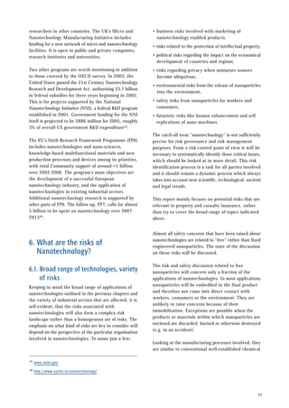
3.2. Sectoral example: Food and
agriculture
Nanotechnology is rapidly converging with biotech and
information technology to radically change food and
agricultural systems. Over the next two decades, the
impacts of nano-scale convergence on farmers and food
could even exceed that of farm mechanisation or of
the Green Revolution according to some sources such
as the ETC group24. Food and nutrition products
containing nano-scale additives are already commercially
available. Likewise, a number of pesticides formulated
at the nano-scale are on the market and have been
released in the environment. According to Helmut
Kaiser Consultancy, some 200 transnational food
companies are currently investing in nanotech and are
on their way to commercialising products25. The US
leads, followed by Japan and China. HKC expects the
nanofood market to surge from $2.6 billion in 2003 to
$7.0 billion in 2006 and to $20.4 billion in 2010.
Companies not associated with food production in the
public mind are already supplying nano-enabled
ingredients to the industry. BASF, for example, exploits
the fact that many vitamins and other substances such
as carotinoids are insoluble in water, but can easily be
mixed with cold water when formulated as
nanoparticles. Many lemonades and fruit juices contain
these specially formulated additives, which can also
be used to provide an ”attractive” color26.
Expected breakthroughs in crop DNA decoding and
analysis could enable agrifirms to predict, control and
improve agricultural production. And with technology
for manipulating the molecules and atoms of food, the
food industry would have a powerful method to design
food with much greater capability and precision, lower
costs and improved sustainability. The combination of
DNA and nanotechnology research could also generate
new nutrition delivery systems, to bring active agents
more precisely and efficiently to the desired parts of
the human body.
Nanotechnology will not only change how every step
of the food chain operates but also who is involved.
At stake is the world’s $3 trillion food retail market,
agricultural export markets valued at $544 billion, the
livelihoods of farmers and the well-being of the rest
of us. Converging technologies could reinvigorate the
battered agrochemical and agbiotech industries, possibly
igniting a still more intense debate – this time over
"atomically-modified" foods.
The most cited nano-agricultural developments are:
Nanoseeds: In Thailand, scientists at Chiang Mai
University's nuclear physics laboratory have rearranged
the DNA of rice by drilling a nano-sized hole through
the rice cell's wall and membrane and inserting a
nitrogen atom. So far, they've been able to change the
colour of the grain, from purple to green.
Nanoparticle pesticides: Monsanto, Syngenta
and BASF are developing pesticides enclosed in
nanocapsules or made up of nanoparticles. The
pesticides can be more easily taken up by plants if
they're in nanoparticle form; they can also be
programmed to be ”time-released.”
Nanofeed for Chickens: With funding from
the US Department of Agriculture (USDA), Clemson
University researchers are feeding bioactive polystyrene
nanoparticles that bind with bacteria to chickens as
an alternative to chemical antibiotics in industrial
chicken production.
Nano Ponds: One of the USA’s biggest farmed fish
17
24 ETC Group ”Down on the Farm: The Impact of Nano-scale Technologies on Food and Agriculture” November 2004
2004 http://www.etcgroup.org/documents/ETC_DOTFarm2004.pdf
25 HKC ”Nanotechnology in Food and Food Processing Industry Worldwide 2003-2006-2010-2015” 2003 .
http://www.hkc22.com/nanofood.html. [The subsequent projections for the world nanofood market may well prove to be underestimates,
given the future purchasing power of senior citizens in developed economies and a world-wide functional food market of
already $70 billion.]
26 BASF ”Improved products, more efficient processes, and new properties”
http://www.corporate.basf.com/en/innovationen/felder/nanotechnologie/nanotech.htm?printview=on&docid=22321&
id=V00-6iy3A6dubbcp-S3](https://image.slidesharecdn.com/44108334-220412124014/85/44108334-pdf-17-320.jpg)