Download to read offline
![Copyright LG Electronics. Inc. All right reserved.
Only for training and service purposes
LGE Internal Use Only- 5 -
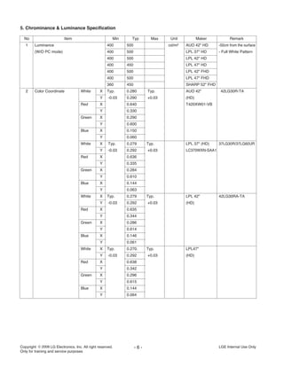
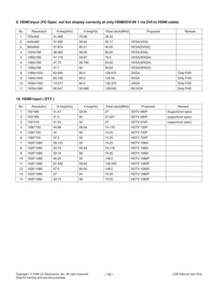
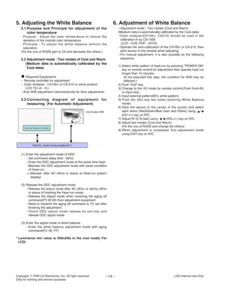
No Item Specification Measurement Result Remark
7. Power Consumption Power on (Blue) : LG30/LG50 Volume: 1/8 volume of
Power on (White) : LG60 sound distortion point
≤ TBD 37" HD
≤ 250W 42" HD
≤ 230W FHD
≤ 320W 47" HD
≤ 310W FHD
≤ 350W 52" FHD
St-By (Red) LG60:St-by Light condition
≤ 1.0 W (All)
8 LCD Module Maker Inch (H)x(V)x(D) unit Remark
(Maker : AUO(HD) Outline Dimension 42" 983 x 576 x 52.7 mm [with inverter]
AUO, CMO, CPT, Pixel Pitch 0.681 x 0.681 mm
LPL, SHARP) Back Light 18 CCFL mm
CMO Outline Dimension 42" - mm
(FHD) Pixel Pitch - mm
Back Light - mm
LPL(HD) Outline Dimension 37" 877 x 516.8 x 55.5 mm [with inverter]
Pixel Pitch 0.200 x 0.600 mm
Back Light 16 EEFL mm
Outline Dimension 42" 983 x 576 x 51 mm [with inverter]
Pixel Pitch 0.227 x 0.681 mm
Back Light mm
Outline Dimension 47" 1096 x 640 x 51 mm [with inverter]
Pixel Pitch 0.76125 x 0.76125 mm
Back Light mm
LPL(FHD) Outline Dimension 42" 983 x 576 x 47.3/(51) mm [w/o inverter]/(with inverter)
Pixel Pitch 0.4845 x 0.4845 mm
Back Light mm
Outline Dimension 47" 1096 x 640 x 50/(51) mm [w/o inverter]/(with inverter)
Pixel Pitch 0.5415 x 0.5415 mm
Back Light mm
SHARP Outline Dimension 52" 1219.0x706.7x64.64 mm (W) x (H) x (D)
(FHD) Pixel Pitch 0.600 x 0.600 mm (H) x (V)
Back Light 24CCFL
Display Colors - -
Coating 3H,AG/ 2H, AG LPL,CMO,AUO / Sharp](https://image.slidesharecdn.com/42lg30r-180129012003/85/42-lg30r-5-320.jpg)
![Copyright LG Electronics. Inc. All right reserved.
Only for training and service purposes
LGE Internal Use Only- 20 -
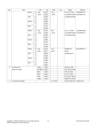
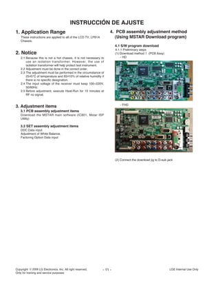
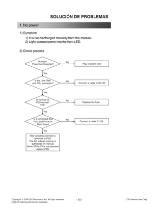
DIAGRAMA DE BLOQUE
AV1in
SideAVin
(AV2in)
Comp1in
Comp2in
RGBin
(D/L)
CVBSIN
Y/Pb/PrIN
R/G/B/HS/VSIN
CVBSIN
LINEOUT
LINE
IN
AMP_MUTE
RS-232CRx/TxMX3232
RF
(Tuner)
PCAudio
in
DISPLAYMODULE
EDIDNVM
EDIDNVM
HDMI1
HDMI2
HDMI3
USB
TMDS351PAG
HDMIMUX
Zoran
VADDIS-966XD
MPEGDecoder
DDRMEM
DDRMEM
SERIAL
FLASH
Mstar
Romeo
LGE6891CD
TW9910
SubDecoder
NTP3000A
Digital
AudioAMP
MAINNVM
MC74HC4066
AudioSW
LM324
X4AMP
SERIAL
FLASH
BD2041
ProtectIC
EDIDNVM
DDC/HDP/CEC
TMDS(HDMIin)
DDC/HPD/CEC
TMDS(HDMIin)
TMDS(HDMIin)
USB(AVI/O,DataI/O)
+5V
CVBS
OUT
656IN
SW_RESE
T
PART_I2
C
PART_I2C
SW_RESE
T
I2SOUT
LVDS
MPEGRX/TX
MPEGRESETI2SIN
656IN
TMDS(HDMIin)
DDC/HPD/CEC
DDC/HPD/CEC
[CECnotthroughHDMIMUX,directJACKtoMAINIC]
DDC
DDC
DDC
UART_Rx/Tx
AUDIO_SWLINE
IN
LINE
IN
LINE
IN
Y/Pb/PrIN
LINE
IN
Y/CIN
LINE
IN
EDIDNVM
ROM_I2C
DSUB_DDC
x0.55
x0.55
x0.55
x0.55S_VIDEO_DETLINE_MUTE
LINEOUT
x4
x0.55LINE
IN
CVBSIN
SIFIN
TUNER_I2C
PART_I2C
HDMI_SEL
(Option)
(Option)
(Option)
SpkOut
1W(Mono)
SW_RESETTPA3107D
AudioAmp](https://image.slidesharecdn.com/42lg30r-180129012003/85/42-lg30r-20-320.jpg)
![Copyright LG Electronics. Inc. All right reserved.
Only for training and service purposes
THE SYMBOL MARK OF THIS SCHEMETIC DIAGRAM INCORPORATES
SPECIAL FEATURES IMPORTANT FOR PROTECTION FROM X-RADIATION.
FILRE AND ELECTRICAL SHOCK HAZARDS, WHEN SERVICING IF IS
ESSENTIAL THAT ONLY MANUFATURES SPECFIED PARTS BE USED FOR
THE CRITICAL COMPONENTS IN THE SYMBOL MARK OF THE SCHEMETIC.
220K
R133
75
R121
75
R111
SD05
D105
220K
R108
COMP1_R
COMP1_Pb
PC_AUD_R
CDS3C05GTA
5.6V
D122
COMP1_Y
SD05
30V
D117
75
R123
5.6V
D103
COMP2_Pr
CDS3C05GTA
5.6V
D123
PPJ209-02
JK100
4A[GN]CONTACT
2A [GN]1P_CAN
3A [GN]O_SPRING
2B [BL]1P_CAN
5B [BL]C_LUG_L
2C [RD]1P_CAN1
5C [RD]C_LUG_L
2D [WH]1P_CAN
5D[WH]C_LUG_L
2E [RD]1P_CAN2
4E[RD]CONTACT
3E [RD]O_SPRING
SD05
D106
5.6V
D104
COMP2_L
220K
R119
COMP1_Pr
COMP1_L
75
R122
75
R110
220K
R106
220K
R120
COMP2_Pb
PPJ209-02
JK101
4A
[GN]CONTACT
2A
[GN]1P_CAN
3A
[GN]O_SPRING
2B
[BL]1P_CAN
5B
[BL]C_LUG_L
2C
[RD]1P_CAN1
5C
[RD]C_LUG_L
2D
[WH]1P_CAN
5D
[WH]C_LUG_L
2E
[RD]1P_CAN2
4E
[RD]CONTACT
3E
[RD]O_SPRING
30V
D119
SD05
1000-ohm
L100
PC_AUD_L
COMP2_R
220K
R132
SD05
30V
D118
1000-ohm
L101
SD05
D107
COMP2_Y
75
R109
5.6V
D115
5.6V
D116
10K
R136
10KR143
10KR144
12K
R142
12K
R145
12K
R137
10K
R134
12K
R135
10K
R138
10K
R140
12K
R139
12K
R141
68R114
DSUB_SCL
75
R116
CDS3C30GTH
30V
D112
DSUB_SDA
+5V_ST
CDS3C30GTH
30V
D110
100
R125
+5V_MULTI
75
R117
DSUB_SDA
DSUB_SCL
0.1uF
C100
PC_G
CDS3C30GTH
30V
D114
0.1uF
C102
75
R118
4.7K
R112
68R115
0.1uF
C101
PC_R
PC_B
PC_VS
68pF
C103
PC_HS
0.1uF
C105
4.7K
R113
68pF
C104
CDS3C30GTH
30V
D113
100
R124
100
R128
4.7K
R150
READY
+5V_ST
100
R129
100
R130
0.1uF
C110
0.1uF
C106
100
R131
OPT
C111
TXD
0.1uF
C108
0.1uF
C109
OPT
C112
RXD
CDS3C30GTH
30V
D121
0.1uF
C107
4.7K
R151
READY
+3.3V_MST
CDS3C30GTH
30V
D120
+5V_ST
ENKMC2837-T112
D109
AAC
C
ENKMC2837-T112
D111
AAC
C
ENKMC2837-T112
D108
AAC
C
MAX3232CDR
IC101
RS232C
3
C1-
2
V+
4
C2+
1
C1+
6
V-
5
C2-
7
DOUT2
8
RIN2
9
ROUT2
10
DIN2
11
DIN1
12
ROUT1
13
RIN1
14
DOUT1
15
GND
16
VCC
PEJ024-01
JK102
6B T_TERMINAL2
8 SHIELD_PLATE
7B B_TERMINAL2
5 T_SPRING
4 R_SPRING
7A B_TERMINAL1
6A T_TERMINAL1
3 E_SPRING
IR_OUT
4.7K
R127
4.7K
R126
6630TGA004K
KCN-DS-1-0089
JK104
1
RED
2
GREEN
3
BLUE
4
GND_1
5
DDC_GND
6 RED_GND
7
GREEN_GND
8 BLUE_GND
9 NC
10 SYNC_GND
11
GND_2
12
DDC_DATA
13
H_SYNC
14
V_SYNC
15
DDC_CLOCK
16 SHILED
KCN-DS-1-0088
JK103
1
2
3
4
5
6
7
8
9
10
AT24C02BN-10SU-1.8
IC100
3
A2
2
A1
4
GND
1
A0
5
SDA
6
SCL
7
WP
8
VCC
1000pF
READY
C113
0
R146
1000pF
READY
C114
0
R147
1000pF
READY
C115
0
R148
1000pF
READY
C116
0
R149
COMPONENT2
SDC 15 applying check
PC SOUND
COMPONENT1
INPUT1 : COMP1/2,RS232C,PC
PC
RS-232C
*ONLY LG30
1.24C02-SUB:0IMMRAL014D
**MULTI ITEM
2.ENKMC2837-SUB:0DS226009AA
(KDS226)
SUB : 0IMCRSG010A(STM)
MAIN : EAN41348201(TI)
*RS232C TX
THE SYMBOL MARK OF THIS SCHEMETIC DIAGRAM INCORPORATES
SPECIAL FEATURES IMPORTANT FOR PROTECTION FROM X-RADIATION.
FILRE AND ELECTRICAL SHOCK HAZARDS, WHEN SERVICING IF IS
ESSENTIAL THAT ONLY MANUFATURES SPECFIED PARTS BE USED FOR
THE CRITICAL COMPONENTS IN THE SYMBOL MARK OF THE SCHEMETIC.
5.6V
D216
220K
R244
SIDE_RIN
75
R241
SD05
D214
SIDE_V
220K
R242
SIDE_LIN
5.6V
D215
75
R245
SIDE_Y
75
R246
SIDE_C
SD05
D217
SD05
D218
S_VIDEO_DET
SD05
D219
12K
R248
12K
R250
10KR247
10KR249
OPT
C210
READY
PPJ218-01
JK204
5C [RD]CONTACT
2C [RD]U_CAN
4C [RD]O_SPRING
2B [WH]U_CAN
3B [WH]C_LUG
2A [YL]U_CAN
5A [YL]CONTACT
4A [YL]O_SPRING
PSJ015-02
JK205
5 O_SPRING
4A C_LUG_L_1
4B C_LUG_S_1
4C C_LUG_L_2
4D C_LUG_S_2
3 GROUND
7SHIELD
0.1uF
16V
READY C213
0
R252
0
R251
100pF
50V
READY
C214
100pF
50V
READY
C215
INPUT2 : CVBS,SIDE AV
SIDE AV
THE SYMBOL MARK OF THIS SCHEMETIC DIAGRAM INCORPORATES
SPECIAL FEATURES IMPORTANT FOR PROTECTION FROM X-RADIATION.
FILRE AND ELECTRICAL SHOCK HAZARDS, WHEN SERVICING IF IS
ESSENTIAL THAT ONLY MANUFATURES SPECFIED PARTS BE USED FOR
THE CRITICAL COMPONENTS IN THE SYMBOL MARK OF THE SCHEMETIC.
TMDS3_RX2-
TMDS3_RXC-
HPD_S/W_2
TMDS2_RXC-
1K
R319
+5V_HDMI_2
HDMI_SEL1
TMDS3_RXC-
HDMI_C-
HDMI_SCL
HDMI_0-
10K
R351
HPD_MST_2
TMDS3_RX0+
TMDS2_RX2-
HDMI_C+
TMDS1_RX0+
+5V_HDMI_3
4.7KR362
CEC_C
DDC_SCL1
CEC
TMDS1_RX1-
HDMI1_5V_DET
TMDS2_RX1+
HDMI3_5V_DETTMDS2_RXC-
TMDS2_RXC+
0.01uFC310
1K
R344
SIDE_HDMI
10K
R300
0.01uFC315
HDMI_0+
+3.3V_MULTI_MST
1K
R310
+3.3V
CEC
DDC_SDA2
0.01uFC314
TMDS3_RX2+
TMDS1_RXC-
HDMI_1-
0.01uFC316
10K
R328
HPD_S/W_1
TMDS2_RX0+
TMDS2_RX0+
0.01uFC308
TMDS3_RX0-
HDMI_2-
HPD_S/W_3
TMDS3_RX0-
TMDS3_RX1+
HDMI2_5V_DET
10K
R324
0
READY
R369
TMDS3_RXC+
DDC_SCL3
TMDS1_RXC+
+3.3V_MULTI_MST
+5V_HDMI_2
HPD_S/W_2
HPD_MST_1
CEC
BSS83
Q306
S
B
D
G
10K
R335
SIDE_HDMI
TMDS1_RX1+
TMDS3_RX1-
TMDS2_RXC+
0
R370
READY
TMDS1_RX2+
4.7K
R375
READY
0
R373
TMDS2_RX1+
TMDS1_RX0-
+3.3V_HDMI_SW
+5V_ST
4.7KR361
0
R356
TMDS2_RX2-
+5V_HDMI_1
TMDS3_RX2-
TMDS3_RX2+
0
R358
HDMI_1+
0.01uF
50V
READY
C307
TMDS2_RX0-
TMDS2_RX0-
TMDS1_RX1-
4.7K
R374
KDS184S
KDS184
D300
A2
C
A1
10K
R329
TMDS2_RX1-
TMDS3_RX0+
0.01uFC311
0.01uFC312
TMDS1_RX2-
+5V_HDMI_3
TMDS3_RX1-
TMDS2_RX2+
HDMI_2+
HDMI_SEL2
TMDS1_RX2+
+5V_HDMI_1
10K
R352
TMDS3_RX1+
0.01uFC309
0
R357
TMDS1_RXC-
0
R355
+5V_ST
TMDS3_RXC+
+5V_HDMI_3
+5V_ST
10K
R301
TMDS1_RX2-
+3.3V_HDMI_SW
+5V_HDMI_1
TMDS1_RX0-
TMDS2_RX1-
TMDS1_RX1+
HPD_S/W_1
0
R368
READY
10K
R325
0
R347
CEC
HDMI_SDA
DDC_SCL2
+5V_HDMI_2
HPD_S/W_3
TMDS1_RX0+
TMDS2_RX2+
0
R345
KDS184S
KDS184
D303
A2
C
A1
DDC_SDA1
0
R346
TMDS1_RXC+
CDS3C30GTH
30V
D302
READY
HPD_MST_3
DDC_SDA3
KDS184S
KDS184
D301
A2
C
A1
0
R350
47K
R330
47K
R331
47K
R326
47K
R327
47K
R354
47K
R353
0READY
R365
0READY
R376
MMBD301LT1G
30V
D304
A
C
DDC_SDA2
DDC_SCL2
DDC_SDA1
DDC_SCL1
DDC_SDA3
DDC_SCL3
TMDS351PAG
IC302
1SDA3
2SCL3
3GND_1
4B31
5A31
6VCC_1
7B32
8A32
9GND_2
10B33
11A33
12VCC_2
13B34
14A34
15GND_3
16VSADJ
17Y4
18Z4
19VCC_3
20Y3
21Z3
22GND_4
23Y2
24Z2
25VCC_4
26Y1
27Z1
28GND_5
29SCL_SINK
30SDA_SINK
31HPD_SINK
32S1
33 S2
34 EQ
35 HPD1
36 SDA1
37 SCL1
38 B11
39 A11
40 VCC_5
41 B12
42 A12
43 GND_6
44 B13
45 A13
46 VCC_6
47 B14
48 A14
49VDD
50HPD2
51SDA2
52SCL2
53B21
54A21
55VCC_7
56B22
57A22
58GND_7
59B23
60A23
61VCC_8
62B24
63A24
64HPD3
0
READY
R383
0.01uF
50V
C301
0.01uF50V
C313
0.01uF50V
C300
51K
R333
30KR334
READY
4.7K
1%
R372
JP1115
JP1116
JP1117
JP1118
JP1119
JP1120
2SC3875S
RT1C3904-T112
Q300
E
B
C
2SC3875S
RT1C3904-T112
Q301
E
B
C
2SC3875S
Q307
SIDE_HDMI
E
B
C
DC1R019NBH
JK303
SIDE_HDMI
14 NC
13 CEC
5 DATA1_SHIELD
20
JACK_GND
12 CLK-
11 CLK_SHIELD
2 DATA2_SHIELD
19 HPD
18+5V_POWER
10 CLK+
4 DATA1+
1 DATA2+
17DDC/CEC_GND
9 DATA0-
8 DATA0_SHIELD
3 DATA2-
16 SDA
7 DATA0+
6 DATA1-
15 SCL
47K
R371
+3.3V
200
R332
QJ41193-FEE2-7F
JK302
1 DATA2+
2 DATA2_SHIELD
3 DATA2-
4 DATA1+
5 DATA1_SHIELD
6 DATA1-
7 DATA0+
8 DATA0_SHIELD
9 DATA0-
10 CLK+
11 CLK_SHIELD
12 CLK-
13 CEC
14 NC
15 SCL
16 SDA
17 DDC/CEC_GND
18 +5V_POWER
19 HPD
20 JACK_GND
21 .
22
.
QJ41193-FEE2-7F
JK301
1
DATA2+
2 DATA2_SHIELD
3 DATA2-
4 DATA1+
5 DATA1_SHIELD
6
DATA1-
7 DATA0+
8 DATA0_SHIELD
9 DATA0-
10 CLK+
11 CLK_SHIELD
12 CLK-
13 CEC
14 NC
15 SCL
16 SDA
17 DDC/CEC_GND
18 +5V_POWER
19 HPD
20 JACK_GND
21
.
22
.
AT24C02BN-10SU-1.8
IC300
3
A2
2
A1
4
GND
1
A0
5
SDA
6
SCL
7
WP
8
VCC
AT24C02BN-10SU-1.8
IC301
3
A2
2
A1
4
GND
1
A0
5
SDA
6
SCL
7
WP
8
VCC
AT24C02BN-10SU-1.8
IC303
SIDE_HDMI
3
A2
2
A1
4
GND
1
A0
5
SDA
6
SCL
7
WP
8
VCC
+5V_MULTI
KDS184S
KDS184
D305
A2
C
A1
+5V_ST
0
R359
READY
4.7K
R360
READY
+3.3V_MULTI_MST
100
R323
100
R322
100R320
100R321
100R348
100R349
22R378
22
R377
22R382
22R381
22R379
22R380
4.7K
READY
R366
*TI Recommand
- > P u l l u p
OPTION
SW_HPD : USE SW HPD (Default)
MST_HPD : USE MST HPD
**MULTI ITEM
1.24C02-SUB:0IMMRAL014D
2.SMD HDMI Jack-SUB:6612B00015B
HDMI
THE SYMBOL MARK OF THIS SCHEMETIC DIAGRAM INCORPORATES
SPECIAL FEATURES IMPORTANT FOR PROTECTION FROM X-RADIATION.
FILRE AND ELECTRICAL SHOCK HAZARDS, WHEN SERVICING IF IS
ESSENTIAL THAT ONLY MANUFATURES SPECFIED PARTS BE USED FOR
THE CRITICAL COMPONENTS IN THE SYMBOL MARK OF THE SCHEMETIC.
EAM38769502L402
EAM38769502
L406
BG1608B121F
EAM38769502
L403
KRC102S
Q403
NOT LG60 E
B
C
IR_OUT
100
R410
NOT LG60
LED_R_PWM_Big
SDA_LED
AC_DET
+3.3V_MST
SPK-N
LED_R/PWM3.3KR417
READY
4.7K
R420
47pF
C403
BG1608B121F
EAM38769502L400
LED_G
10K
R434
NOT LG60
+5V_ST
0.1uF
C408
KEY2
KEY1
470pF
C404
4.7K
R421
0.1uF
C411
3.3KR435
NOT LG60
0
READY
R425
OPT
C407
470pF
C412
10K
R409
READY
SCL_LED
+5V_ST
EYEQ_RESET
470pF
C401
NOT LG60
EAM38769502L401
NOT LG60
22uF
16V
C414
USE LG50_60_70
12505WS-15A00
P400
1
2
3
4
5
6
7
8
9
10
11
12
13
14
16
15
0
R424
HD
TXCE0+,TXCE0-,TXCE1+,TXCE1-,TXCE2+,TXCE2-,TXCE3+,T
4.7K
FHD
R407
+3.3V
2SA1530A-T112-1R
Q402
NOT LG60
E
B
C
3.3KR413
0.1uF
C400
+5V_ST
OPT
READY
C402
10K
R440
IR-OUT
10K
R443
IR-OUT
+5V_ST
10K
R441
IR-OUT
47K
R439
IR-OUT
22
R442
IR-OUT
IR
10KR414
LG60
10K READY
R403
22uF
16V
C406
+3.3V_MST
5.6B
ZD400
LG60
2SC3052
Q405
IR-OUT E
B
C
2SC3052
Q404
IR-OUTE
B
C
PNP
Q406
LG60
E
B
C
+5V_ST_SW
3.3K
R445
LG60
3.3K
R444
LG60
0
READY
R415
0
NOT LG60
R404
0
R405
UBW2012-121F
120OHM
L404
UBW2012-121F
120OHM
L407
USE LG50_60_70
BG1608B501F
L410
BEAD_USE LG50_60_70
BG1608B501F
L411
BEAD_USE LG50_60_70
0L411-*1
R_USE LG50_60_70
0L410-*1
R_USE LG50_60_70
5.6B
ZD401
USELG50_60_70
5.6B
ZD402
USELG50_60_70
0R423
USE LG50_60_70
0R422
USE LG50_60_70
TXCE2-
TXCO1-
TXCO0-
TXCO3-
TXCE3-
TXCO4-
TXCLKE-
TXCO2-
TXCE1-
TXCE0-
TXCE4-
TXCLKO-
CONTRO
NOT LG60
PANEL WAFER
*LG6 Sound module output
FHD 8BIT:NC
FHD 8BIT:NC
X
R407 R424
HD
FHD X
O
4.7K](https://image.slidesharecdn.com/42lg30r-180129012003/85/42-lg30r-22-320.jpg)
![Copyright LG Electronics. Inc. All right reserved.
Only for training and service purposes
THE SYMBOL MARK OF THIS SCHEMETIC DIAGRAM INCORPORATES
SPECIAL FEATURES IMPORTANT FOR PROTECTION FROM X-RADIATION.
FILRE AND ELECTRICAL SHOCK HAZARDS, WHEN SERVICING IF IS
ESSENTIAL THAT ONLY MANUFATURES SPECFIED PARTS BE USED FOR
THE CRITICAL COMPONENTS IN THE SYMBOL MARK OF THE SCHEMETIC.
100R507
READY
+5V_TUNER
0.027uF
C512
4.7uF
35V
C510
READY
AM_AUDIO
27pF
C502
4.7K
R503
0.01uF
C503
+5V_TUNER
0.1uF
C520
+5V_TUNER
0R545
220
R522
270pF
C513
READY
1K
R513
27pF
C501
MAIN_SIF
1KR515
TV_MAIN
0.01uF
C507
READY
OPT
READY R553
SCL_TUNER
SDA_TUNER
+5V_TUNER
4.7K
R504
4.7K
R508
0
R514
330R506
330R505
4700pF
C506
220
R521
2SA1530A-T112-1R
Q502
E
B
C
RT1C3904-T112
Q501
E
B
C
0R519
0R518
TAFT-Z703D
TU500
NON EU TUNER
14 AFT
13 V-OUT
5 RF_AGC
12 NC_4
11 AS
2 GND_1
19 NC_7
18 NC_6
10 CLOCK
4 NC_2
1 NC_1
17 NC_5
9 DATA
8 GND_2
3 +B[5V]
16 SIF-OUT
7 NC_3
6 TP[33V_OPTION]
15 A-OUT
21
SHIELD
20 NC_8
BLM18BD102SN1D
L502
READY
TAFT-H703F
TU500-*1 NTSC TUNER
14
AFT
13
V-OUT
5
RF_AGC
12
NC_4
11
AS
2
GND_1
19
NC_7
18
NC_6
10
CLOCK
4
NC_2
1
NC_1
17
NC_5
9
DATA
8
GND_2
3
+B[5V]
16
SIF-OUT
7
NC_3
6
TP[33V_OPTION]
15
A-OUT
21
SHIELD
20
NC_8UBW2012-121F
120OHM
L501
10uF
16V
C521
N e a r t h e p i n
TUNER
THE SYMBOL MARK OF THIS SCHEMETIC DIAGRAM INCORPORATES
SPECIAL FEATURES IMPORTANT FOR PROTECTION FROM X-RADIATION.
FILRE AND ELECTRICAL SHOCK HAZARDS, WHEN SERVICING IF IS
ESSENTIAL THAT ONLY MANUFATURES SPECFIED PARTS BE USED FOR
THE CRITICAL COMPONENTS IN THE SYMBOL MARK OF THE SCHEMETIC.
0.1uF
C641
+5V_MULTI
SW_R
680K
R637
+5V_MULTI
+5V_MULTI
2.2uFC662
+5V_MULTI
680K
R640
4.7K
R633
SW_L
4.7K
R634
MC74HC4066ADR2G
IC602
3
YB
2
YA
4
XB
1
XA
6
CONTROL_C
5
CONTROL_B
7
GND
8
XC
9
YC
10
YD
11
XD
12
CONTROL_D
13
CONTROL_A
14
VCC
C
680K
R638
680K
R639
680K
R629
2.2uFC665
680K
R630
680K
R612
680K
R611
AUDIO_SW
+5V_MULTI
2.2uFC664
+5V_MULTI
COMP1_L
+5V_MULTI
SIDE_LIN
2.2uFC663
R64
+1.8V_DVDD
0.1uF
C605
0.1uF
C617
10uF 16V
C604
+1.8V_DVDD
0.1uF
C636
4.7K
R623
1uF
C608
1000pF
C630
0.1uF
C602
1000pF
C620
I2S_SDO
0.1uF
C629
+16V_NTP
NTP3000A
IC600
1BST1A
2VDR1A
3/RESET
4AD
5VSS_IO
6CLK_I
7CLK_O
8VDD_IO
9DGNDPLL
10AGNDPLL
11LFM
12AVDDPLL
13DVDDPLL
14NC_1
15DVSS
16
DVDD
17
SDATA
18
WCK
19BCK
20
SDA
21
SCL
22
PWM_3B/PWM_HP2
23
PWM_3A/PWM_HP1
24
PROTECT
25
FAULT
26
VDR2B
27
BST2B
28
PGND2B_1
29 PGND2B_2
30 OUT2B_1
31 OUT2B_2
32 PVDD2B_1
33 PVDD2B_2
34 PVDD2A_1
35 PVDD2A_2
36 OUT2A_1
37 OUT2A_2
38 PGND2A_1
39 PGND2A_2
40 BST2A
41 VDR2A
42 NC_2
43VDR1B
44BST1B
45PGND1B_1
46PGND1B_2
47OUT1B_1
48OUT1B_2
49PVDD1B_1
50PVDD1B_2
51
PVDD1A_1
52
PVDD1A_2
53
OUT1A_1
54
OUT1A_2
55PGND1A_1
56PGND1A_2
22000pFC623
0.1uF
C637
1uFC624
10uF 16V
C600
+3.3V
100pF
C601
SCL_Part
1000pF
C635
1000pF
C634
330uF35V
C612
1000pF
C631
0
HOTEL_OPT
R642
100
R601
+16V_NTP
1000pF
C606
+16V_NTP
+16V_NTP
100
R602
I2S_MCLK
+1.8V_AVDD
0.01uF
C613
10uF16V
C609
100pF
READY
C642
DA-8580
EAP38319001
L603
2S
1S 1F
2F
22000pF
C616
0.1uF
C607
3.3K
R600
1000pF
C603
+16V_NTP
+1.8V_AVDD
AC_DET
100
R603
0.47uF
C632
1uFC618
1000pF
50V
C651
3.3
R604
0.1uF
C615
4.7K
R624
1000pF
C621
0.1uF
C626
+16V_NTP
0.1uF
C610
22000pF
C625
1000pF
C622
1000pF
C619
I2S_SCK
I2S_WS
SDA_Part
22000pFC611
D
EAP
L
2S
1S
SW_RESET
AMP_MUTE_HOTEL
3.9
R607
3.9
R609
3.9
R608
3.9
R610
3.9
R622
3.9
R618
3.9
R617
3.9
R621
330uF 35V
C666
RT1C3904-T112
Q600
E
B
C
1uF
C614
30V
READY
D600
30V
READY
D601
30V
READY
D602
30V
READY
D603
0R606
2SA1530A-T112-1R
Q608
E
B
C
+3.3V_MST
10K
R650
100
R651
33pF
50V
C667
READY
33pF
50V
C668
READY
1N4148W
100V
D604
READY1N4148W
100V
D605
READY
1N4148W
100V
D606
READY
1N4148W
100V
D607
READY
for COMP1
for S
Audio S/W : COMP1 or SIDE L/R
Digital Audio AMP
THE SYMBOL MARK OF THIS SCHEMETIC DIAGRAM INCORPORATES
SPECIAL FEATURES IMPORTANT FOR PROTECTION FROM X-RADIATION.
FILRE AND ELECTRICAL SHOCK HAZARDS, WHEN SERVICING IF IS
ESSENTIAL THAT ONLY MANUFATURES SPECFIED PARTS BE USED FOR
THE CRITICAL COMPONENTS IN THE SYMBOL MARK OF THE SCHEMETIC.
+3.3VDDA
RAMRAS
RAMCS
I2S_DIN
RAMDQM
JP703
RAMBA[0]
0.1uF
50V
C750
4.7K
R716
150R728
IPCLK
MX25L1605AM2C-15G
IC703
IC703_USB
3
WP#
2
SO
4
GND
1CS#
5
SI
6
SCLK
7
HOLD#
8 VCC
JP702
+1.8VDDC
RAMADD[0-3]
DUPRD0
SFDI
+3.3VDDP
0R722
+1.8VDDA
RAMWE
0R723
0.1uF50V
C732
+1.8VDDCMBW3216-501TF
L715
+3.3VDDP
27
R700
100uF
16V
C722
SFCLK
SFDO
0.1uF
C717
RAMADD[10]
0.1uF
C713
0
R740
READY
DEC_656[0]
USB_DN
22pFC745
0.1uF50V
C742
0.1uF
50V
C753
0.1uF
50V
C748
1K
R709
0
R741
READY
1/10W
1K
5%
R704
+3.3VDDP
0.1uF
C716
0.1uF
50V
C752
0R725
5pF
50V
C709
RAMRAS
RAMBA[1]
0.1uF50V
C739
SFDO
4.7K
R706
1/10W
1K
5%
R705
RAMBA[1]
0R717
0.1uF50V
C730
10uF
16V
C724
27
R701
+3.3VDDP
USB_DN
0R720
0.1uF50V
C729
RAMDQM
75R737
+3.3VDDP
390
R733
15K
1%
R726
TX_MPEG
+1.8V
0.1uF50V
C738
RAMCAS
12MHz
X702
SFCS
+3.3VDDP
+3.3VDDP
27MHz
X703
0.1uF50V
C728
0R739
SFCLK
+3.3V_USB
0.1uF
C712
0.1uF50V
C726
+1.8VDDA
0.1uF50V
C736
RAMBA[0]
JP701
220K
R732
USB_DP
+3.3VDDA
USB_DP
DUPRD0
0.1uF50V
C731
0R719
+3.3VDDP
0.1uF50V
C727
SFDI
75R734
RAMCAS
0.1uF
C725
75R736
0.1uF
50V
C723
SFCS
RAMCS
RAMADD[11]
0.1uF
50V
C747
5.1K
READY
R702
IPCLK
47uF
16V
C714
RAMADD[4-9]
I2S_WS_IN
+1.8VDDC
0R724
DEC_656_CLK
5.1K
READY
R703
0.1uF50V
C744
0R721
+1.8VDDA
0.1uF
50V
C749
MPEG_RESET
RAMDAT[8-15]
+5V_USB
SFCLK
0R718
RAMWE
SFDI
I2S_CLK_IN
0.1uF
50V
C751
RAMADD[0-11]
75R735
22pFC746
0.1uF50V
C743
+3.3VDDA
RAMDAT[0-7]
0.1uF
50V
C734
JP700
DEC_656[0-7]
0.1uF50V
C737
0.1uF50V
C741
1/10W
0
5%
R738
0.1uF50V
C740
+3.3V_SDRAM
0.1uF50V
C735
RX_MPEG
RAMDAT[0-15]
1/10W
56
5%
R707
22uF
16V
C710
22uF
16V
C711
22uF
16V
C715
ZR36966PQCG-XD
IC707
USB1
2
3
4
5
6
7
8
9
10
11
12
13
14
15
16
17
18
19
20
21
22
23
24
25
26
27
28
29
30
31
32
33
34
35
36
37
38
39
40
41
42
43
44
45
46
47
48
49
50
51
52
53
54
55
56
57
58
59
60
61
62
63
64
65
66
67
68
69
70
71
72
73
74
75
76
77
78
79
80
81
82
83
84
85
86
87
88
89
90
91
92
93
94
95
96
97
98
99
100
101
102
103
104
105
106
107
108
109
110
111
112
113
114
115
116
117
118
119
120
121
122
123
124
125
126
127
128
HY57V641620FTP
IC704
26
A3
27
VDD3
28
VSS1
29
A4
30
A5
31
A6
32
A7
33
A8
34
A9
35
A11
36
NC1
37
CKE
38
CLK
39
UDQM
40
NC2
41
VSS2
42
DQ8
43
VDDQ3
44
DQ9
45
DQ10
46
VSSQ3
47
DQ11
48
DQ12
49
VDDQ4
50
DQ13
17
CAS
3
VDDQ1
6
VSSQ1
16
WE
15
LDQM
14
VDD2
13
DQ7
12
VSSQ2
11
DQ6
10
DQ5
9
VDDQ2
8
DQ4
7
DQ3
4
DQ1
5
DQ2
25
A2
24
A1
23
A0
2
DQ0
22
A10/AP
21
BA1
1
VDD1
20
BA0
19
CS
18
RAS
51
DQ14
52
VSSQ4
53
DQ15
54
VSS3
USBDOWNSTREAM
KJA-UB-4-0004
P701
USB
12345
+3.3VDDP
4.7K
READY
R742
OPT
L716
READY
4.7K
READY
R743
+5V_MULTI
12505WS-04A00
JK700
1
2
3
4
5
6.19KR715
OCP_EN
22R744
OCP_EN
FLASH_WP_ZORAN
+3.3VDDP
10K
R710
180
R708
10nF
50V
C754
READY
1K
R727
18pFC720
18pFC719
200
R729
READY
MIC2009YM6-TR
IC705
3
ENABLE
2
GND
4
FAULT/
1
VIN
6
VOUT
5
ILIMIT
120OHM
UBW2012-121F
L711
120OHM
UBW2012-121F
L712
120OHM
UBW2012-121F
L713
120OHM
UBW2012-121F
L714
120OHM
UBW2012-121F
READY
L717
120OHM
UBW2012-121F
L718
MLF2012A2R7JT000
L719
READY 220pF
50V
C755
READY
75R712
75R711
75R714
75R713
RAMADD[6]
DEC_656[5]
RAMADD[1]
RAMADD[8]
RAMDAT[7]
RAMADD[2]
DEC_656[3]
RAMDAT[6]
RAMADD[3]
RAMDAT[0]
RAMADD[9]
RAMDAT[12]
RAMDAT[5]
RAMADD[8]
DEC_656[2]
RAMDAT[10]
RAMDAT[2]
RAMDAT[4]
RAMADD[9]
RAMDAT[11]
RAMDAT[14]
DEC_656[6]
RAMDAT[7]
DEC_656[4]
RAMDAT[14]
RAMDAT[1]
RAMDAT[0]
RAMADD[11]
RAMDAT[13]
RAMDAT[13]
RAMDAT[4]
RAMDAT[8]
RAMDAT[10]
RAMDAT[3]
RAMDAT[12]
RAMADD[2]
RAMADD[6]
DEC_656[0]
RAMADD[0]
RAMADD[5]
RAMADD[3]
RAMDAT[8]
RAMDAT[15]
RAMADD[7]
RAMADD[4]
RAMADD[4]
RAMADD[5]
RAMDAT[9]
DEC_656[1]
RAMADD[1]
RAMADD[0]RAMADD[7]
RAMDAT[5]
RAMDAT[15]
RAMDAT[9]
RAMDAT[2]
RAMDAT[1]
RAMADD[10]
RAMDAT[6]
RAMDAT[11]
DEC_656[7]
RAMDAT[3]
** 1A Design
* R732 Video Output Level Reference
C709 :EMI Solution
p l a c e d a s c l o s e t o C o n n e c t o r a s p o s s i b l e .
External F/W Download
Capacitors on VBUSA should be
F o r I n i t i a l D o w n l o a d
DEC_656[0] : DUPTD0
* Analog Video Option
ZORAN I2C strobe ready
DUPTD0
* R715 Recommendation is 6.19k 1%
Originally 392 ohm 1%
DEBUG TEST OPTION
* R732 Video Output Level Refere nc
t o m e e t U S B 2 . 0 H S c e r t
ZORAN SRAM Board F/W Download
I t ’ s p o s s i b e l t o 2 7 ~ 4 7 o h m
C o n n e c t t o M a i n I C ( C C I R 6 5 6 I n t e r f a c e )
TOP SIDE!
USB/MPEG DEC
THE SYMBOL MARK OF THIS SCHEMETIC DIAGRAM INCORPORATES
SPECIAL FEATURES IMPORTANT FOR PROTECTION FROM X-RADIATION.
FILRE AND ELECTRICAL SHOCK HAZARDS, WHEN SERVICING IF IS
ESSENTIAL THAT ONLY MANUFATURES SPECFIED PARTS BE USED FOR
THE CRITICAL COMPONENTS IN THE SYMBOL MARK OF THE SCHEMETIC.
PC_AUD_L
4.7uF
C834
1N4148W
100V
D800
READY
PC_VS
2.2uFC849
MAIN_SIF
+3.3V_MULTI_MST
HWRESET
CVBS_RIN
+5V_ST
SIDE_Y
COMP2_L
SIDE_C
2.2uFC845
COMP1_Pb
PC_HS
PIP_VOUT
20pFC841
MNT_VOUT_T
1uFC837
SW_L
+3.3V_MULTI_MST
PC_AUD_R
CVBS_VIN
SIDE_V
2.2uFC847
2.2uFC842
+3.3V_MULTI_MST
+3.3V_MULTI_MST
COMP2_Pr
2.2uFC846
SW_R
+3.3V_MULTI_MST
COMP1_Pr
PC_G
2.2uFC843
PC_R
COMP2_Y
COMP2_R
+3.3V_MULTI_MST
MNT_R_AMP
2.2uFC839
2.2uFC848
MNT_L_AMP
PC_B
CVBS_LIN
2.2uFC840
COMP2_Pb
COMP1_Y
1M
R8064
20pFC838
+3.3V_MULTI_MST
14.31818MHz
X800
0.1uF
C804
READY
TV_MAIN
AM_AUDIO
10uF
16V
C833
KDS181
D802
100
R8018
100
R8019
4.7uF
10V
C800
33K
R8016
0.1uF
50V
C824KDS181
D801
AC_RST
HWRESET
+3.3V_MST
0
R8002
I2S_MCLK
I2S_WS
I2S_SCK
I2S_SDO
I2S_WS_IN
I2S_CLK_IN
I2S_DIN
0R8027
READY
0R8022
READY
0R8028
READY0R8023
READY
0R8024
READY
0R8029
READY
0R8026
READY
22R8053
READY
22R8052
READY
22R8055
22R8056
100R8078
READY
100R8075
READY
100R8077
100R8074
100R8085
100R8082
100R8087
100R8089
100R8095
100R8092RS232C
100R8094RS232C
0.047uFC813
0.047uFC817
0.047uFC816
0.047uFC814
0.047uFC819
0.047uFC812
0.047uFC815
0.047uFC818
0.047uFC810
0.047uFC820
0.047uFC823
0.047uFC822
0.047uFC829
0.047uFC827
0.047uFC830
0.047uFC828
0.047uFC825
0.047uFC826
0.047uFC831
0.1uFC832
0.1uF
C835
0.1uFC836
0.1uFC844
1000pFC811
1000pFC821
PANEL_ON
SDA_TUNER
RXD
TXD
HPD_MST_3
HPD_MST_2
HDMI_0+
HDMI_0-
HDMI_C-
HDMI_C+
HDMI_SCL
HDMI_2-
HDMI_SDA
HDMI_2+
HDMI_1-
HDMI_1+
HPD_MST_1
47R8031
47R8012
47R8043
47R8036
47R8037
47R8047
47R8032
47R8013
47R8046
47R8034
47R8041
47R8033
47R8038
47R8035
47R8044
47R8030
47R8045
47R8049TW9910 block
47R8017
47R8011
47R8039
47R8042
0.1uF
C809
0.1uFC807
0.1uFC806
0.1uFC808
0R8025
READY
2.2KR8071
READY
0.1uFC859
0.1uFC852
0.1uFC850
47R8048OPT
22KR8084
22KR8088
0.1uFC805
10KR8076
390R8054
HDMI_SEL2
HDMI_SEL1
100R8015
100R8065
100R8066
SCL_TUNER
HDMI2_5V_DET
HDMI3_5V_DET
HDMI1_5V_DET
+3
4.7KR8181
0
R8000
OPT
402
R8020
4021%
R8004
OPT
PIP_VOUTPIP_V
402
R868
OPT
1608
68
R8007
OPT
470
R8006
OPT
75
R8014
402
R870
470
R8050
DCDC_7.22V_PIP
MNT_VOUT_T
1608
68
R8051
+3.3V_MST
4.7K
R8174
4.7K
READY
R8173
TMUE312GAB
SW800
1
2 4
3
5
0.1uFC882
0.1uFC881
2SA1530A-T112-1R
Q801
OPT
E
B
C
2SA1530A-T112-1R
Q804
TW9910 block
E
B
C
RT1C3904-T112
Q802
OPTE
B
C
RT1C3904-T112
Q805E
B
C
0.1uF
16V
C880
LGE699
IC80
FHD
1RXB1N
2RXB1P
3GND_3
4RXB2N
5RXB2P
6HPLUGB
7DDCDB_DA
8DDCDB_CK
9RXACKN
10RXACKP
11GND_11
12RXA0N
13RXA0P
14AVDD_33_14
15RXA1N
16RXA1P
17GND_17
18RXA2N
19RXA2P
20HPLUGA
21REXT
22DDCDA_DA
23DDCDA_CK
24HSYNC1
25VSYNC1
26VCLAMP
27REFP
28REFM
29BIN1P
30SOGIN1
31GIN1P
32RIN1P
33VCOM3
34BIN0P
35VCOM2
36GIN0P
37SOGIN0
38RIN0P
39AVDD_33_39
40GND_40
41HSYNC0
42VSYNC0
43VSYNC2
44BIN2P
45SOGIN2
46GIN2P
47RIN2P
48C1
49Y1
50C0
51Y0
52CVBS3
53CVBS2
54CVBS1
55VCOM1
56CVBS0
57VCOM0
58AVDD_33_58
59CVBSOUT1
60CVBSOUT0
61GND_61
62SIP0P
63AVDD_SIF
64SIF1P
65SIFM
66GND_66
67AUVRADN
68AUVRADP
69AUVREF
70AVDD_AU
71AUL0
72AUR0
73AUL1
74AUR1
75AUCOM
76AUL2
77AUR2
78AUL3
79AUR3
80AUMONO
81AUOUTL3
82AUOUTR3
83AUOUTL2
84AUOUTR2
85AUOUTL1
86AUOUTR1
87AUOUTL0
88AUOUTR0
89GPIOF[0]
90GPIOF[1]
91GPIOF[2]
92GPIOF[3]
93GPIOF[4]
94GPIOF[5]
95GPIOF[6]
96GPIOF[7]
97GPIOF[8]
98GPIOF[9]
99VDDP_99
100GND_100
101VDDC101220LVB0M
221VDDP_221
222GND_222
223GPIOE[3]
224GPIOE[2]
225GPIOE[1]
226GPIOE[0]
227ICLK
228IDE
229IHSYNC
230IVSYNC
231DI[0]
232DI[1]
233DI[2]
234DI[3]
235VDDP_235
236DI[4]
237DI[5]
238DI[6]
239DI[7]
240VDDC_240
241GND_241
242DI[8]
243DI[9]
244DI[10]
245DI[11]
246DI[12]
247DI[13]
248HWRESET
249XOUT
250XIN
251AVDD_MPLL
252RXBCKN
253RXBCKP
254AVDD_33_254
255RXB0N
256RXB0P
LGE6891DD
IC801-*1
HD
1RXB1N
2RXB1P
3GND_3
4RXB2N
5RXB2P
6HPLUGB
7DDCDB_DA
8DDCDB_CK
9RXACKN
10RXACKP
11GND_11
12RXA0N
13RXA0P
14AVDD_33_14
15RXA1N
16RXA1P
17GND_17
18RXA2N
19RXA2P
20HPLUGA
21REXT
22DDCDA_DA
23DDCDA_CK
24HSYNC1
25VSYNC1
26VCLAMP
27REFP
28REFM
29BIN1P
30SOGIN1
31GIN1P
32RIN1P
33VCOM3
34BIN0P
35VCOM2
36GIN0P
37SOGIN0
38RIN0P
39AVDD_33_39
40GND_40
41HSYNC0
42VSYNC0
43VSYNC2
44BIN2P
45SOGIN2
46GIN2P
47RIN2P
48C1
49Y1
50C0
51Y0
52CVBS3
53CVBS2
54CVBS1
55VCOM1
56CVBS0
57VCOM0
58AVDD_33_58
59CVBSOUT1
60CVBSOUT0
61GND_61
62SIP0P
63AVDD_SIF
64SIF1P
65SIFM
66GND_66
67AUVRADN
68AUVRADP
69AUVREF
70AVDD_AU
71AUL0
72AUR0
73AUL1
74AUR1
75AUCOM
76AUL2
77AUR2
78AUL3
79AUR3
80AUMONO
81AUOUTL3
82AUOUTR3
83AUOUTL2
84AUOUTR2
85AUOUTL1
86AUOUTR1
87AUOUTL0
88AUOUTR0
89GPIOF[0]
90GPIOF[1]
91GPIOF[2]
92GPIOF[3]
93GPIOF[4]
94GPIOF[5]
95GPIOF[6]
96GPIOF[7]
97GPIOF[8]
98GPIOF[9]
99VDDP_99
100GND_100
101VDDC_101
102DQS[1]
103MDATA[15]
104MDATA[14]
105GND_105
106MDATA[13]
107MDATA[12]
108VDDM_108
109MDATA[11]
110MDATA[10]
111MDATA[9]
112MDATA[8]
113GND_113
114VDDM_114
115MDATA[7]
116MDATA[6]
117MDATA[5]
118MDATA[4]
119VDDM_119
120MDATA[3]
121MDATA[2]
122MDATA[1]
123MDATA[0]
124DQS[0]
125LDQM
126UDQM
127MVREF
128MCLKE
129 MCLKZ
130 MCLK
131 BADR[1]
132 BADR[0]
133 RASZ
134 GND_134
135 VDDM_135
136 AVDD_MEMPLL
137 CASZ
138 WEZ
139 MADR[0]
140 MADR[1]
141 MADR[2]
142 MADR[3]
143 MADR[4]
144 MADR[5]
145 MADR[6]
146 MADR[7]
147 VDDM_147
148 GND_148
149 VDDC_149
150 MADR[8]
151 MADR[9]
152 MADR[10]
153 MADR[11]
154 AD[0]
155 AD[1]
156 AD[2]
157 AD[3]
158 AD[4]
159 AD[5]
160 AD[6]
161 AD[7]
162 WRZ
163 RDZ
164 ALE
165 VDDP_165
166 GND_166
167 SCK
168 SDI
169 CSZ
170 SDO
171 SAR0
172 SAR1
173 SAR2
174 SAR3
175 PWM0
176 PWM1
177 DDCR_DA
178 DDCR_CK
179 DDCA_DA
180 DDCA_CK
181 INT
182 IRIN
183 VDDP_183
184 GND_184
185 VDDC_185
186 GPIOB[4]
187 GPIOB[5]
188 GPIOB[6]
189 NC_189
190 NC_190
191 PWM2
192 PWM3
193VDDC_193
194VDDP_194
195NC_195
196NC_196
197LVA3P
198LVA3M
199LVACKP
200LVACKM
201LVA2P
202LVA2M
203LVA1P
204LVA1M
205LVA0P
206LVA0M
207VDDP_207
208GND_208
209NC_209
210NC_210
211LVB3P
212LVB3M
213LVBCKP
214LVBCKM
215LVB2P
216LVB2M
217LVB1P
218LVB1M
219LVB0P
220LVB0M
221VDDP_221
222GND_222
223GPIOE[3]
224GPIOE[2]
225GPIOE[1]
226GPIOE[0]
227ICLK
228IDE
229IHSYNC
230IVSYNC
231DI[0]
232DI[1]
233DI[2]
234DI[3]
235VDDP_235
236DI[4]
237DI[5]
238DI[6]
239DI[7]
240VDDC_240
241GND_241
242DI[8]
243DI[9]
244DI[10]
245DI[11]
246DI[12]
247DI[13]
248HWRESET
249XOUT
250XIN
251AVDD_MPLL
252RXBCKN
253RXBCKP
254AVDD_33_254
255RXB0N
256RXB0P
SPK-N2.2KR8183
0
TW9910 block
R8081
100R8010
DCDC_7.22V_PIP
FLASH_WP
0R8080
0R8079
1000pFC853
1000pFC854
0
READY
R8021
0
READY
R8057
0R8058
100R8073
100R8072
HPD_MST_2
S_VIDEO_DET
1000pFC851
100
R8060
+3.3V_MST
4.7K
R8091
4.7K
READY
R8090
0.1uFC801
0.1uF
C803
0.1uFC855
DEC_656[0]
DEC_656[1]
DEC_656[2]
DEC_656[3]
DEC_656[4]
DEC_656[5]
DEC_656[6]
DEC_656[7]
TXCO4+
NON_EU OPTION
MSTAR
CVBS_V
SW_L/R: COMP2_L/R or SIDE_L/R
RS232C
MSTAR Recommand
: o v e r 8 V
GAIN X 4
GAIN X 4
H/W OPTION #3
120HZ: H
Normal: L](https://image.slidesharecdn.com/42lg30r-180129012003/85/42-lg30r-23-320.jpg)
![Copyright LG Electronics. Inc. All right reserved.
Only for training and service purposes
THE SYMBOL MARK OF THIS SCHEMETIC DIAGRAM INCORPORATES
SPECIAL FEATURES IMPORTANT FOR PROTECTION FROM X-RADIATION.
FILRE AND ELECTRICAL SHOCK HAZARDS, WHEN SERVICING IF IS
ESSENTIAL THAT ONLY MANUFATURES SPECFIED PARTS BE USED FOR
THE CRITICAL COMPONENTS IN THE SYMBOL MARK OF THE SCHEMETIC.
MADR[4]
0.1uF
C903
MADR[1]
MADR[11]
MADR[9]
SBA0
MADR[2]
150READY R903
LDQM
CKE
MADR[2]
MADR[3]
MDATA[0-15]
MADR[9]
MCLK
MADR[7]
MADR[5]
1000pF
C907
MADR[6]
0.1uF
C904
+2.5V_VDDM_MST
0.1uF
C906
0.1uF
C909
WEZ
+2.5V_VDDM_MST
UDQM
0.1uF
C905
MADR[0]
CASZ
DQS1
1K
R906
MADR[3]
MADR[0-11]
MADR[4]
MADR[8]
150
R905
MADR[0]
MADR[1]
1K
R909
MCLKZ
0.1uF
C901
SBA1
MADR[8]
MADR[6]
DQS0
RASZ
0.1uF
C908
MADR[11]
MADR[10]
MADR[7]
0.1uF
C902
MADR[5]
MADR[10]
0.1uF
C900
1/16W
56
AR903
1/16W
56
AR902
1/16W
56
AR901
1/16W
56
AR900
HYB25DC256163CE-4
IC900
26
BA0
27
BA1
28
A10/AP
29
A0
30
A1
31
A2
32
A3
33
VDD_3
34
VSS_1
35
A4
36
A5
37
A6
38
A7
39
A8
40
A9
41
A11
42
A12/NC_5
43
NC_6
44
CKE
45
CK
46
CK
47
UDM
48
VSS_2
49
VREF
50
NC_7
17
A13/NC_2
3
VDDQ_1
6
VSSQ_1
16
LDQS
15
VDDQ_3
14
NC_1
13
DQ7
12
VSSQ_2
11
DQ6
10
DQ5
9
VDDQ_2
8
DQ4
7
DQ3
4
DQ1
5
DQ2
25
NC_4
24
CS
23
RAS
2
DQ0
22
CAS
21
WE
1
VDD_1
20
LDM
19
NC_3
18
VDD_2
51
UDQS
52
VSSQ_3
53
NC_8
54
DQ8
55
VDDQ_4
56
DQ9
57
DQ10
58
VSSQ_4
59
DQ11
60
DQ12
61
VDDQ_5
62
DQ13
63
DQ14
64
VSSQ_5
65
DQ15
66
VSS_3
MDATA[12]
MADR[4]
MADR[4]
MDATA[11]
MADR[0-11]
MADR[9]
MADR[8]
MADR[11]
MADR[11]
MADR[2]
MDATA[0-15]
MDATA[0-15]
MDATA[1]
MDATA[2]
MDATA[14]
MDATA[0]
MADR[5]
MADR[0]
MADR[6]
MADR[0]
MADR[8]
MADR[10]
MADR[7]
MADR[7]
MADR[10]
MADR[9]
MADR[3]
MDATA[15]
MDATA[5]
MDATA[7]
MDATA[10]
MADR[1]
MADR[6]
MDATA[9] MDATA[6]
MADR[5]
MADR[1]
MADR[2]
MADR[3]
MDATA[3]
MDATA[4]
MDATA[8]
MDATA[13]
DDR
**MULTI ITEM
SUB - HYNIX : EAN31729202
MAIN - QIMONDA : EAN41788501
THE SYMBOL MARK OF THIS SCHEMETIC DIAGRAM INCORPORATES
SPECIAL FEATURES IMPORTANT FOR PROTECTION FROM X-RADIATION.
FILRE AND ELECTRICAL SHOCK HAZARDS, WHEN SERVICING IF IS
ESSENTIAL THAT ONLY MANUFATURES SPECFIED PARTS BE USED FOR
THE CRITICAL COMPONENTS IN THE SYMBOL MARK OF THE SCHEMETIC.
SCL_Part
75
R1000
R1
PIP_V
0.1uF
C1000
+1.8V
+1.8V_AVD
T
1VDDE_1
2SCLK
3SDAT
4PDN
5RSTB
6TMODE
7NC_1
8AVD_1
9YMUX3
10YMUX2
11YGND
12YMUX1
+3.3V
SDA_Part
0.01uFC1001
100R1003
100R1002
0.1uFC1004
0.1uFC1002
0.1uFC1003
SW_RESET
+3.3V
4.7K
R1001READY
100R1004
4.7K
R1006
R1007
0.
C1
22pFC1005
THE SYMBOL MARK OF THIS SCHEMETIC DIAGRAM INCORPORATES
SPECIAL FEATURES IMPORTANT FOR PROTECTION FROM X-RADIATION.
FILRE AND ELECTRICAL SHOCK HAZARDS, WHEN SERVICING IF IS
ESSENTIAL THAT ONLY MANUFATURES SPECFIED PARTS BE USED FOR
THE CRITICAL COMPONENTS IN THE SYMBOL MARK OF THE SCHEMETIC.
0.1uF
C1135
22uH
L1101
AZ1117H-ADJTRE1(EH11A)
IC1104
2
OUTPUT
3INPUT 1 ADJ/GND
2.7K
R1126
READY
PANEL_STATUS
AZ1117H-ADJTRE1(EH11A)
IC1101
2
OUTPUT
3INPUT 1 ADJ/GND
DCDC_7.22V_PIP
22K
R1130
P_12V
402
1%
R1144
7.5K
R1120
1.2K
R1190
+1.2V_VDDC_MST
0.1uF
C1102
MP2355DN-LF-Z
IC1102
3
VIN
2
BST
4
LX
1
SS
5
GND
6
FB
7
COMP
8
RUN
+5V_MULTI
110
1%
R1123
0.1uF
C1101
10K
R1189
P_5V
47uF25V
C1137
0.1uF
C1140
P_16V
10KR1135
P_5V
AC_RST0R1125
P_5V
10uF
16V
C1107
0.01uF
C1103
RL_ON
10K
R1133
10K
R1134
2.2uF
25V
C1125
DC_DIM
+5V_MULTI
0
READY
R1191
+2.5V_VDDM_MST
3.3K
1%
R1166
+5V_ST
SI4925DY
0TF492509AA
Q1101
3S2
2
G1
4
G2
1
S1
5
D2_1
6 D2_2
7
D1_1
8 D1_2
365
1%
R1137
0.1uF
C1115
0.1uF
C1136
0R1132
100uF
16V
C1110
AZ1117H-ADJTRE1(EH11A)
IC1103
2
OUTPUT
3INPUT 1 ADJ/GND
+5V_ST
12K
R1110
100uF
16V
C1105
0.01uF
C1144
+12V
4.7K
R1122
NOT SHARP 32&52",AUO
P_12V
220uF
16V
C1138
0.1uF
C1142
100uF
16V
C1149
0
R1115
SC4215ISTRT
IC1100
3VIN
2
EN
4
NC_2
1
NC_1
5
NC_3
6
VO
7
ADJ
8
GND
P_5V
59K
R1111
1uF
C1124
1uF 25V
C1126
330
1%
R1124
+5V_ST
100uF16V
C1109
PANEL_ON
+5VST_MST
220uF
16V
C1100
100uF
16V
C1119
+5V_ST
0.1uF
C1139
+12V
0
READY
R1188
I_DIMMING DISP_EN
P_16V
10K
R1128
51
5%
R1165
0.01uF
C1150
RL_ON
100uF
16V
C1118
AC_DET SAM2333
D1106
+5V_MULTI
100uF16V
C1128
0.1uF
C1111
0.01uF
C1106
47
R1102
1.6K
R1131
2.2uF
25V
C1116
+5VST_MST
0.1uF
C1148
4.7K
R1138
0.47uF
C1121
E_DIMMING
2700pF
50V
C1113
MBRS190T3G
90V
D1103
+5V_TUNER
0.47uF
C1114
NOT SHARP 52",AUO
P_16V
0.01uF
C1108
+5V_ST
10K
R1129
0.01uF
C1146
100uF
16V
C1141
1K
R1192
0.1uF
C1112
+3.3V_MST
P_12V
10K
R1184
MBW3216-501TF
L1100
+16V_NTP
RT1C3904-T112
Q1100
E
B
C
2SC3875S
Q1102
1
2
3
RT1C3904-T112
Q1107
E
B
C
RT1C3904-T112
Q1106
E
B
C
SMAW200-24C
P1100
19Power ON
14 GND
95V
4 GND
18 ACD
13GND
8 GND
3GND
17Error out
12 5V
7GND
2 16V
16 AGND
115V
6 12V
116V
20 Inverter ON
15GND
10 5V
512V
21A.Dim 22 PWMDim
23Select 24 SYNC
MBR230LSFT1G
30V
D1100
5.6K
R1107
18K
R1106 33K
R1140
33K
R1141
2.2K
R1152
2.2K
R1154
2.2K
R1153
330
1%
R1194
USB
100uF
16V
C1151
USB
+5V_USB
AZ1117H-ADJTRE1(EH11A)
IC1107
USB
2
OUTPUT
3INPUT 1 ADJ/GND
0.1uF
C1120
USB
110
1%
R1195
USB
1/10W
100
5%
R1139-*1
PWM_DIM
1/10W
1K
5%
R1139
DC_DIM
0
R1163
S2A
D1102
50V
10uF
C11524.7uF
C1117
10K
READY
R1196
0
SHARP 52",AUO
R1197
0 CMO 32,42,47R1185
0
NOT (CMO 32,42,47,57, SHARP 32")
R1183
0CMO 57"
R1187
0 CMO 57"R1186
0
NOT CMO 57"
R1127
0
CMO 32,42,47,57
R1155
+5V_MULTI
0R1105
0
NOT CMO 32,42,47,57
R1104
0
CMO 32,42,47,57
R1103
0.1uF
C1154
100uF
16V
C1153
+5V_MULTI MBW3216-501TF
L1103USB
0.1uF
C1130
USB
1R1148
+3.3V_HDMI_SW
+3.3V_USB
22uF
16V
C1129
USB
+3.3V_SDRAM
0.1uF
C1156
+3.3V
10uF16V
C1133
TW9910 block
0.1uF
C1131
0.1uF
C1147
47uF
16V
C1145
0.01uF
C1132
0
R1149
+3.3V_MULTI_MST
47uF
16V
C1155
+1.8V
+12V
P_5V
EAM38769505
UBW2012-121F
L1104
120OHM
READY
L1108
EAM38769505
UBW2012-121F
L1105
L1107
UBW2012-121F
MBW3216-501TF
L1109
UBW2012-121F
120OHM
32Sharp
L1110
UBW2012-121F
120OHM
NOT32Sharp
L1111
P_5V
VCC_LCD
AZ1117H-3.3
IC1105
2
OUTPUT
3INPUT 1 ADJ/GND
AZ1117H-3.3
IC1108
2
OUTPUT
3INPUT 1 ADJ/GND
0
5%
R1168
0
5%
R1170
OPT
R1167
READY
OPT
R1169
READY
AZ1117H-1.8TRE1(EH13A)
IC1106
2
OUTPUT
3INPUT 1 ADJ/GND
OPT
R1150
READY
0
5%
R1151
0.1uF
C1122
0.1uF
C1123
UBW2012-121F
EAM38769505
L1106
MBW3216-501TF
EAM30764101
L1112
0.01uF
C1134
22uF
16V
C1104
+5VST_MST
+5V_USB
+12V
OUT:2.6V
( 8 )
110mA
LED Block
12V->5V_TUNER
DC-DC CONVERTER
ST 5V->3.3V->1.2V
R1
SWITCH VCC_LCD:12V or 5V
OUT:1.25V
R2
e q u a l t o 2 2 0 u F p a d s i z e
5V:5V_PULLUP,5V_MULTI
OUT:UNDER 7.22V
SWITCH 5V->3.3V->1.8V
20mA
SWITCH 5V->DDR 2.5V
MAX1A
MAX1A
MAX1A
R2
R1
R1
R1
R2
R2
V0 = 0.8(R1+R2) / R2
*Applied to SIF,HDMI,ADC,MPLL,AUD
*3.3V_NTP,TW9910,ETC.
*NTP.USB,TW9910
*12V AUDIO and PANEL
*SHARP 32" : DC DIMMING
R1122
Sharp 52"
AUO
X
4.7K
O
R1197
CMO 32/42/47
O
O
CMO 57"
X
X
C1114
X
R1127
X
X
O
O
the Rest(w/CMO26") O
O
X
4.7K
4.7K
0.47uF
X
0.47uF
0.47uF
X
R1183
O
OX
O
R1155
O
X
X
X
X
X
X
R1185
O
R1103
O
O X
R1186
O
X
X
X
X
X
X
R1187
O
X
X
X
X
X
O
X
X
O
O
R1104
*PANEL OPTION
XSharp 32" XXXX X OX X X X
PPWER](https://image.slidesharecdn.com/42lg30r-180129012003/85/42-lg30r-24-320.jpg)

This document is a service manual for an LG LCD television. It contains safety precautions, specifications, adjustment instructions, troubleshooting information, block diagrams, exploded views and other service-related content. Safety warnings are provided at the beginning, noting high voltages present and precautions that must be taken when servicing the device. Technical specifications for the television such as screen size, resolution, power requirements and more are detailed. The manual provides information needed for technicians to properly service the television.


![[Leaflet] LY540 leaflet for better person.pdf](https://cdn.slidesharecdn.com/ss_thumbnails/leafletly540sasia-250117215121-aefe7480-thumbnail.jpg?width=640&height=640&fit=bounds)


