
Recommended
More Related Content
What's hot
What's hot (20)
Similar to Semiconductivity-priya
Similar to Semiconductivity-priya (20)
Recently uploaded
Recently uploaded (20)
Semiconductivity-priya
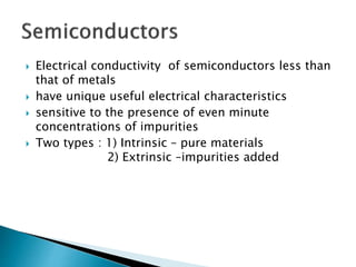
- 1. Electrical conductivity of semiconductors less than that of metals have unique useful electrical characteristics sensitive to the presence of even minute concentrations of impurities Two types : 1) Intrinsic – pure materials 2) Extrinsic –impurities added
- 2. band structure relatively narrow forbidden band gap (<2 eV) Eg : Si (1.1eV) and Ge(0.7eV) Also compounds composed of Groups IIIA and VA – GaAs, In Sb Groups IIB and VIA- Cd S, Zn Te
- 3. In above compounds , ->dissimiar electronegativities -> atomic bonding becomes more ionic -> band gap energy increases—more insulative
- 4. a vacant electron state in the VB created because of e- from VB excited to CB Treating a missing electron from the valence band as a positively charged particle called a hole. Charge of hole= +1.6x10^-19 C In the presence of an electric field, excited electrons and holes move in opposite directions
- 6. Two types of charge carrier (free electrons and holes) p is the number of holes per cubic meter µh is the hole mobility ni is known as the intrinsic carrier concentration
- 7. impurity concentration determines the electrical behavior of semiconductors One atom in 10^12 is sufficient to render silicon extrinsic at room temperature. Types : 1) n-type 2) p-type
- 8. Si has 4 e-s : covalent bonded with other adjacent atoms If we add a Grp VA impurity , 4e-s form bonds , there will be 1 e- free . It is free e- / conducting e- For these free e-s , energy state is in forbidden band gap just below CB If energy is given,e- get excited to CB Hence this type impurity is termed a ‘donor’ No hole in VB
- 9. At room temp, we can easily excite large no. of e-s from donor states No.of e-s in CB >>no.of holes in VB This type material is n-type extrinsic semiconductors e- are majority carriers Holes are minority charge carriers n-type : Fermi level shifted upward in band gap