Supercapacitors and Battery power management for Hybrid Vehicles
•
1 like•979 views

1. The document presents a study on using multi-boost and full-bridge converters for power management in hybrid electric vehicles combining supercapacitor and battery power sources. 2. Two converter topologies - multi-boost and multi-full bridge - are investigated for their suitability in distributing power from multiple supercapacitor modules to the vehicle's DC bus. Control strategies are developed for each topology. 3. Simulation and experimental results are presented for setups using 2 boost converters or 1 full-bridge converter, showing the converters can balance currents between supercapacitor modules and maintain the battery current level as required.
![2
Supercapacitors are storage devices which enable to supply the peaks of power to hybrid vehicle
during the transient states. During the steady states, batteries will provide the energy requested. This
methodology enables to decrease the weight and increases the lifespan of the batteries. Hybridization
using batteries and super capacitors [1] for transport applications is needed when energy and
power management are requested during the transient sates and steady states. The multi boost
and multi full bridge converters will be investigated because of the high power.
For range problems, traction batteries used until now cannot satisfy the energy needed
for future vehicles. To ensure a good power management in hybrid vehicle, the multi boost and
multi full bridge converters topologies and their control are developed. Two topologies proposed
for the power management in ECCE Hybrid Vehicle are presented in Fig.1.
(a) First solution
Figure 1. Converter topologies for ECCE Hybrid Vehicle
2. DC/DC Converters Topologies and Modelling
2.1. Multi boost and Multi full bridge converters modelling
• Figure 2a shows the multi boost converter topology. The general model for this topology [2] is
given by equation (1); where (α1) and (n) define respectively the duty cycle and parallel input
converter number.
⋅+=
−=⋅
+⋅⋅⋅⋅++=⋅
⋅⋅⋅⋅=
⋅−=⋅
Lbatch
bus1batbat
busnbus2bus1bus1L
p
bus11scnscnn
IkII
VV)(I
dt
dλ
PPPVI
N,,2,1n
VαV)(I
dt
dL
(1)
The voltage drops in the Ln and λ inductances are given by equation (2).
⋅=
⋅=
)(I
dt
dλ
λ
V
)(I
dt
dLV
bat
scnnLn
(2)
(b) Second solution
Authorized licensed use limited to: Vignan's Engineering College. Downloaded on February 21,2010 at 06:56:10 EST from IEEE Xplore. Restrictions apply.](data:image/gif;base64,R0lGODlhAQABAIAAAAAAAP///yH5BAEAAAAALAAAAAABAAEAAAIBRAA7)
Recommended
Recommended
More Related Content
What's hot
What's hot (20)
Viewers also liked
Viewers also liked (20)
Similar to Supercapacitors and Battery power management for Hybrid Vehicles
Similar to Supercapacitors and Battery power management for Hybrid Vehicles (20)
More from Pradeep Avanigadda
More from Pradeep Avanigadda (13)
Recently uploaded
Recently uploaded (20)
Supercapacitors and Battery power management for Hybrid Vehicles
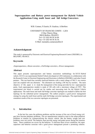
- 1. 1 Supercapacitors and Battery power management for Hybrid Vehicle Applications Using multi boost and full bridge Converters M.B. Camara, F.Gustin, H. Gualous, A.Berthon UNIVERSITY OF FRANCHE COMTE – L2ES 13 Rue Thierry Mieg 90010 Belfort, FRANCE Tel:+33/ (0)3 84 58 36 04. Fax:+33/ (0)3 84 58 36 36. E-Mail: mamadou.camara@utbm.fr Acknowledgment This study is sponsored by Electronic and Electrical Engineering Research Center (CREEBEL) in BELFORT, FRANCE. Keywords «Supercapacitors», «Boost converter», «Full bridge converter», «Power management» Abstract This paper presents supercapacitors and battery association methodology for ECCE Hybrid vehicle. ECCE is an experimental Hybrid Vehicle developed at L2ES Laboratory in collaboration with the Research Center in Electrical Engineering and Electronics in Belfort (CREEBEL) and other French partners. This test bench has currently lead-acid batteries with a rated voltage of 540 V, two motors each one coupled with one alternator. The alternators are feeding a DC-bus by rectifers. The main objective of this paper is to study the management of the energy provides by two supercapacitor packs. Each supercapacitors module is made of 108 cells with a maximum voltage of 270V. This experimental test bench is carried out for studies and innovating tests for the Hybrid Vehicle applications. The multi boost and multi full bridge converter topologies are studied to define the best topology for the embarked power management. The authors propose a good power management strategy by using the multi boost and the multi full bridge converter topologies. The experimental and simulation results of the two converter topologies are presented. 1. Introduction In the last few years the pollution problems and the increase of the cost of fossil energy (oil, gas) have become planetary problems. The car manufacturers started to react to the urban pollution problems in nineties by commercializing the electric vehicle. But the battery weight and cost problems were not solved. The batteries must provide energy and peaks power during the transient states. These conditions are severe for the batteries. To decrease these severe conditions, the super capacitors and batteries associate with a good power management present a promising solution. Authorized licensed use limited to: Vignan's Engineering College. Downloaded on February 21,2010 at 06:56:10 EST from IEEE Xplore. Restrictions apply.
- 2. 2 Supercapacitors are storage devices which enable to supply the peaks of power to hybrid vehicle during the transient states. During the steady states, batteries will provide the energy requested. This methodology enables to decrease the weight and increases the lifespan of the batteries. Hybridization using batteries and super capacitors [1] for transport applications is needed when energy and power management are requested during the transient sates and steady states. The multi boost and multi full bridge converters will be investigated because of the high power. For range problems, traction batteries used until now cannot satisfy the energy needed for future vehicles. To ensure a good power management in hybrid vehicle, the multi boost and multi full bridge converters topologies and their control are developed. Two topologies proposed for the power management in ECCE Hybrid Vehicle are presented in Fig.1. (a) First solution Figure 1. Converter topologies for ECCE Hybrid Vehicle 2. DC/DC Converters Topologies and Modelling 2.1. Multi boost and Multi full bridge converters modelling • Figure 2a shows the multi boost converter topology. The general model for this topology [2] is given by equation (1); where (α1) and (n) define respectively the duty cycle and parallel input converter number. ⋅+= −=⋅ +⋅⋅⋅⋅++=⋅ ⋅⋅⋅⋅= ⋅−=⋅ Lbatch bus1batbat busnbus2bus1bus1L p bus11scnscnn IkII VV)(I dt dλ PPPVI N,,2,1n VαV)(I dt dL (1) The voltage drops in the Ln and λ inductances are given by equation (2). ⋅= ⋅= )(I dt dλ λ V )(I dt dLV bat scnnLn (2) (b) Second solution Authorized licensed use limited to: Vignan's Engineering College. Downloaded on February 21,2010 at 06:56:10 EST from IEEE Xplore. Restrictions apply.
- 3. 3 (a) Figure 2. (a): Multi boost Converter topology, (b): Multi full bridge converter topology The converter average model has a nonlinear behavior because of crosses between α1 control variable and Vbus1 parameter. The Vbus1, Vsc1, Vsc2, Vscn , Ich and Vbat variables can to disturb the control, they must be measured and used in the estimate of the control law to ensure a dynamics of control [3]. The multi boost converter [4] topology control law which results from the boost converter modeling is presented by α1 duty cycle (3); where Np = max(n) is the maximum number of parallel converters. λbat LnL2L1scnsc2sc1 p 1 VV )VV(V)VV(V N 1 1α − +⋅⋅⋅++−+⋅⋅⋅++ ⋅−= (3) The multi boost converter control strategy is presented in Fig.3 (a). It ensures the super capacitor modules discharge with variable current. The super capacitors reference current (Iscref) is obtained starting from the power management between batteries and hybrid vehicle DC-link. This control strategy includes the super capacitors and batteries current control loops. PWM1 signal ensures the multi boost converters control during super capacitor modules discharge. These modules being identical, the energy management between the modules and the hybrid vehicle DC-link enables to write the super capacitors current references (4). +⋅⋅⋅++= −⋅ ⋅ ⋅= +⋅⋅⋅++= screfnscref2scref1scref batrefch scn bus1 p screfn scnsc2sc1sc IIII )II( Vη V N 1I IIII (4) To simplify the super capacitors current references estimation, the multi boost converter efficiency (η) was fixed at 85%. • The multi full bridge converter [5] control strategy proposed in this paper consists to establish the full bridge converters standardized voltage [6]. The control law which result from the multi full bridge converter modeling is presented by equation(5), where (m) defines the transformer turns ratio. (b) Authorized licensed use limited to: Vignan's Engineering College. Downloaded on February 21,2010 at 06:56:10 EST from IEEE Xplore. Restrictions apply.
- 4. 4 +⋅⋅⋅++ = ⋅ − ⋅≈ p scnsc2sc1 scn scn λbat mod N VVV V Vη VV m 1U (5) This standardized voltage is compared with two triangular carrier waves of amplitude Vmax = 1V with a switching frequency of 20 kHz. The inverter control strategy is presented in Fig. 3(b); where Q1, Q2, Q3 and Q4 are the control signals applied to K1, K2, K3 and K4 switches. The simulations and experimental parameters are presented in table below. (a) Multi boost control strategy Figure 3. Multi boost and Multi full bridge converters control strategy 2.2 Full bridge converter simulation results for Np = 2 The simulation has been made for Np = 2 [7] . The maximum and minimum voltages of the super capacitor modules are respectively fixed at 270V and 135V. The hybrid vehicle requested current (Ich) is respectively fixed at 100A from 0 to 0.5s, 400A from 0.5s to 18s and 100A from 18s to 20s. Battery reference current (Ibatref) is fixed at 100A independently of the hybrid vehicle power request. Super capacitor modules voltages (Vsc1, Vsc2) presented in Fig.4 (a) are identical. The currents amplitudes (Isc1, Isc2) presented in Fig.4 (b) are also identical. Control enables to maintain the battery current (Ibat) at 100A; but around 0.5s and 18s the battery current control loop has not enough time to react Fig.5 (a). The important power of the transient states is ensured by the super capacitors modules (IL) Fig. 5(b). Simulation parameters are presented in TABLE I. TABLE I: FULL BRIDGE TOPOLOGIE SIMULATIONS PARAMETERS Symbol Value Name λ 25µH Battery current smoothing inductance m 3 Planar transformer turns ratio Vbus1 604V-432V DC-link voltage L1=L2 50µH Super capacitors currents smoothing inductances (a) Figure 4. (a): Super capacitor modules voltages, (b): Super capacitor modules currents (b) Multi full bridge control strategy (b) Authorized licensed use limited to: Vignan's Engineering College. Downloaded on February 21,2010 at 06:56:10 EST from IEEE Xplore. Restrictions apply.
- 5. 5 (a) Figure 5. (a): Battery current control result, (b): DC-link and active load currents 3. Design and Experimental results Wiring in power electronic design is a general problem for electrical energy system and the voltage inverters do not escape to this problem. The switch action of semiconductors causes instantaneous fluctuations of the current and any stray inductance in the commutation cell will produce high voltage variations. Semiconductors, when switching off, leads to high voltage transitions which is necessary to control within tolerable limits. The energy stored in parasitic inductances, during switching on, is generally dissipated by this semiconductor. In the case of the single-phase inverter, each cell includes two switches and a decoupling capacitor placed at the cell boundaries, which presents a double role. It enables to create an instantaneous voltage source very close to the inverter. The (C) capacitor associated to an inductor enables to filter the harmonic components of the currents which are generated by the inverter. Parasitic inductances staying in the mesh include the capacitor inductance, the internal inductance of semiconductors and the electric connection inductances. A good choice of the components with an optimal wiring enables to minimize parasitic inductances. Using the semiconductors modules solves the connection problems between components. All these efforts can become insufficient, if residual inductances remain too high or if the inverter type is the low voltages and strong currents for which the voltage variations are much important. In both cases, the use of the chopping devices is necessary. These devices must be placed very close to the component to avoid any previous problem. The parameters used for experimental tests are presented in TABLE II and the principle of such circuits [8] is given in Fig. 6. TABLE II: FULL BRIDGE EXPERIMENTAL PARAMETERS Symbol Value Name R1= R2=R3 = R4 10Ω Chopping circuits resistances C1=C2=C3=C4 220µF Chopping circuits capacitors λ 25µH Battery current smoothing inductance m 3 Planar transformer turns ratio Vbus1 60V-43V DC-link voltage C 6800 µF Super capacitors voltage smoothing capacitor L1 50µH Super capacitors currents smoothing inductance (b) Authorized licensed use limited to: Vignan's Engineering College. Downloaded on February 21,2010 at 06:56:10 EST from IEEE Xplore. Restrictions apply.
- 6. 6 Figure 6. Full bridge converter with chopping devices During switching off of the semiconductors, the corresponding current stored in wiring inductances circulates in the following meshes C1, D1 ; C2 , D2; C3, D3 and C4 , D4 which limits the voltages applied to the switches. When electrical energy is fully transferred in C1, C2, C3 and C4 capacitors, the current becomes null and the meshes become closed. The C1, C2, C3 and C4 capacitors are used only for transient energy tank and it is necessary to recycle this switching energy while controlling the voltage at the semiconductors boundary. This function is ensured by R1, R2, R3 and R4 resistances. R1, R2, R3 and R4 resistances are identical and C1, C2, C3 and C4 capacitors are also identical. 3.1 Experimental setup at reduced scale (a) Boost converters setup for Np = 2 Figure 7. Boost and full bridge converters experimental setup For reasons of cost components and safety, the experimental test benches were carried out at a reduced scale (1/10). • The boost converter test bench Fig.7 (a) is made of: a battery module of 4 cells in series, two super capacitors modules of 10 cells (Maxwell BOOSTCAP2600) in series for each one, an active load which is used to define power request, two boost converters in parallel which ensure power management in hybrid vehicle. • For the full bridge converter [9] test bench Fig.7 (b), a batteries module, a super capacitors module, two high frequency planar transformer, the DC/AC and AC/DC converters have been designed. The super capacitors modules voltages must be between 27 V and 13.5 V. The batteries module which imposes the DC-bus voltage presents a rated voltage of 48 V and the DC- link voltage level must be between 43 V and 60 V. The converters are controlled by a PIC18F4431 microcontroller with 10 kHz control frequencies for boost converters and 20 kHz for the full bridge converter. (b) Full bridge converter setup for Np = 1 Authorized licensed use limited to: Vignan's Engineering College. Downloaded on February 21,2010 at 06:56:10 EST from IEEE Xplore. Restrictions apply.
- 7. 7 3.1. Boost converters simulation and experimental results The boost converters experimental test is carried out in the following conditions: During the super capacitors discharge, the batteries current reference (Ibatref) is fixed at 13A so that, the super capacitors modules provide hybrid vehicle power request during the transient states. For these tests, the hybrid vehicle request (Ich) was fixed at 53A. The experimental and simulations results of the modules voltage are compared in Fig.8 (a) and Fig.8 (b). The (Isc1) and (Isc2) experimental currents are not identical Fig.9 (a), Fig.9 (b) because the super capacitors dispersion and the power electronic circuits (boost converters) inequality. The first boost converter ensures 50% and the second ensures also 50% of the DC-link current (IL). In other words the two super capacitors modules ensure a (IL) current of 40A to hybrid vehicle as presented in Fig.10 (a), and 13A only is provided by the batteries Fig.10 (b). (a) First module voltage Figure 8. Super capacitor modules experimental and simulation voltage results (a) First module current Figure 9. Super capacitor modules experimental and simulation current results (a) Multi boost output current (IL ) Figure 10. DC-link voltage and current experimental validation (b) Second module voltage (b) Battery current experimental result (b) Second module current Authorized licensed use limited to: Vignan's Engineering College. Downloaded on February 21,2010 at 06:56:10 EST from IEEE Xplore. Restrictions apply.
- 8. 8 3.2.Full bridge converters experimental results The Q1, Q2, Q3 and Q4 control signals [10] applied to K1, K2, K3 and K4 semiconductors are presented in Fig.11(a). For electric constraints reasons of the available components, (transformer, IGBT, active load), the full bridge experimental test conditions are different to that of boost converters topology. The super capacitors module maximum voltage (Vsc1) is fixed at 22V because of battery module voltage (48V), the transformer turns ratio (m=3) and active load which is limited to 80V. The battery current reference (Ibatref) and active load current request (Ich) are respectively fixed at 5A and 15A. The DC-link experimental voltage is presented in Fig.11 (b). The super capacitors power is not constant (Vsc1, Isc1) because of the consumed current by R1, R2, R3 and R4 resistances Fig.12 (a). The battery current experimental result is presented in Fig.12 (b). The voltages and currents ripples which appear in Fig. 11 (b), Fig.12 (a) and Fig. 12 (b) are caused by leakage inductances of the transformer and wiring of the power electronics devices. (a) Figure 11. (a): Full bridge control signals, (b): Battery and DC-link experimental voltages (a) Figure 12. (a): Super capacitors module voltage and current, (b): DC-link and active load experimental currents (a) Transformer input and output voltages Figure 13. (a):High frequency planar transformer voltages and currents (b) (b) Transformer input and output currents (b) Authorized licensed use limited to: Vignan's Engineering College. Downloaded on February 21,2010 at 06:56:10 EST from IEEE Xplore. Restrictions apply.
- 9. 9 The voltages and currents of the high frequency planar transformer are respectively presented in Fig. 13 (a) and Fig. 13 (b). The transformer secondary voltage (Vs2) transient which corresponds to the change of sign of the current (Is2) is caused by the transformer leakage inductance. 4. Conclusion In this paper, multi boost and multi full bridge converter topologies and their control strategies for batteries and super capacitors coupling in the hybrid vehicle applications were proposed. The system control is ensured by PIC18F4431 microcontroller type which includes 9 analog inputs and 8 PWM outputs. For reasons of simplicity and cost, the multi boost converter is the most interesting topology regarding the multi full bridge converter topology. It enables a good power management in hybrid vehicle. Full bridge experimental tests conditions were different from that of boost converter topology, so at this time it is not easy to make a good comparison between the two topologies. However, multi full bridge converter topology is well suitable to adapt the level of available voltage to the DC-link. For low voltage and high current applications such as super capacitors, the full bridge converter seems to be less interesting because of its higher cost ( many silicon and passive components), and a lower efficiency. References [1] J.M Timmermans, P. Zadora, J. Cheng, Y. Van Mierlo, and Ph. Lataire. Modelling and design of super capacitors as peak power unit for hybrid electric vehicles. Vehicle Power and Propulsion, IEEE Conference, 7-9 September, page 8pp, 2005. [2] Huang jen Chiu, Hsiu Ming Li-Wei Lin, and Ming-Hsiang Tseng. A multiple- input dc/dc converter for renewable energy systems. ICIT2005, IEEE, 14-17 December, pages 1304–1308, 2005. [3] M.B. Camara, H. Gualous, F. Gustin, and A. Berthon. Control strategy of hybrid sources for transport applications using supercapacitors and batteries. IPEMC2006, 13-16 August, Shanghai, P.R.CHINA, 1:1–5, 2006. [4] L. Solero, A. Lidozzi, and J.A. Pomilo. Design of multiple-input power converter for hybrid vehicles. IEEE transactions on power electronics, 20, Issue 5, 2005. [5] Xin KONG and A. KHA. Analysis and implementation of a high efficiency, interleaved current-fed full bridge converter for fuel cell system. IEEE, 28-01 Nov, 1:474–479, 2005. [6] M.B. Camara, F. Gustin, H. Gualous and A. Berthon. Studies and realization of the buck-boost and full bridge converters with multi sources system for the hybrid vehicle applications. Second European Symposium on Super capacitors and Applications, ESSCAP2006, Lausanne, Switzerland,2-3 November, 2006. [7] Huang-Jen Chiu, Hsiu-Ming, Li-Wei Lin, Ming-Hsiang Tseng. A Multiple-Input DC/DC Converter for Renewable Energy Systems, Industrial Technology, ICIT2005, IEEE international Conference, 14-17 December 2005, Pages:1304-1308 [8] LOUNIS Zohra. APPOTS DES TECHNIQUES DE CABLAGES LAMINAIRES DANS UN ONDULEUR A IGBT DE MOYENNE PUISSANCE. PhD thesis, Institut National Polytechnique de Lorraine, 2000. [9] Seong-Jeub Jeon, Gyu-Hyeong Cho. A Zero-Voltage and Zero-Current Switching Full Bridge DC-DC Converter With Transformer Isolation, IEEE Transactions on power Electronics, Vol.16, No.5, September 2001, Pages:573-580 [10] Yungtaek Jabg, Milan M.Jovanovic, Yu-Ming Chang. A New ZVS-PWM Full-Bridge Converter, IEEE Transactions on power Electronics, Vol.18, No.5, September 2003, Pages:1122-1129 Authorized licensed use limited to: Vignan's Engineering College. Downloaded on February 21,2010 at 06:56:10 EST from IEEE Xplore. Restrictions apply.