SlideShare a Scribd company logo
1 of 750
Download to read offline
The Patent Office Journal 27/02/2015 26366
पेटेंट कायालय
शासक य जनल
OFFICIAL JOURNAL
OF
THE PATENT OFFICE
िनगमन सं. 09/2015 शुबवार दनांक: 27/02/2015
ISSUE NO. 09/2015 FRIDAY DATE: 27/02/2015
पेटेंट कायालय का एक ूकाशन
PUBLICATION OF THE PATENT OFFICE
The Patent Office Journal 27/02/2015 26367
INTRODUCTION
In view of the recent amendment made in the Patents Act, 1970 by the Patents (Amendment) Act, 2005
effective from 01st
January 2005, the Official Journal of The Patent Office is required to be published under
the Statute. This Journal is being published on weekly basis on every Friday covering the various proceedings
on Patents as required according to the provision of Section 145 of the Patents Act 1970. All the enquiries on
this Official Journal and other information as required by the public should be addressed to the Controller
General of Patents, Designs & Trade Marks. Suggestions and comments are requested from all quarters so that
the content can be enriched.
(Chaitanya Prasad)
CONTROLLER GENERAL OF PATENTS, DESIGNS & TRADE MARKS
27th
FEBRUARY, 2015
The Patent Office Journal 27/02/2015 26368
CONTENTS
SUBJECT PAGE NUMBER
JURISDICTION : 26369 – 26370
SPECIAL NOTICE : 26371 – 26372
EARLY PUBLICATION (DELHI) : 26373 – 26374
EARLY PUBLICATION (MUMBAI) : 26375 – 26388
EARLY PUBLICATION (CHENNAI) : 26389
PUBLICATION AFTER 18 MONTHS (DELHI) : 26390 – 26910
PUBLICATION AFTER 18 MONTHS (MUMBAI) : 26911 – 26912
PUBLICATION AFTER 18 MONTHS (CHENNAI) : 26913 – 27011
PUBLICATION AFTER 18 MONTHS (KOLKATA) : 27012 – 27038
AMENDMENT UNDER SEC. 57 (KOLKATA) : 27039 – 27040
PUBLICATION UNDER SECTION 43(2) IN RESPECT OF
THE GRANT (DELHI) : 27041 – 27045
PUBLICATION UNDER SECTION 43(2) IN RESPECT OF
THE GRANT (MUMBAI) : 27046 – 27047
PUBLICATION UNDER SECTION 43(2) IN RESPECT OF
THE GRANT (CHENNAI)
: 27048 – 27049
PUBLICATION UNDER SECTION 43(2) IN RESPECT OF
THE GRANT (KOLKATA)
: 27050 – 27053
INTRODUCTION TO DESIGN PUBLICATION : 27054
THE DESIGNS ACT 2000 SECTION 30 DESIGN
ASSIGNMENT
: 27055
CANCELLATION PROCEEDINGS UNDER SECTION 19 OF
THE DESIGNS ACT, 2000
: 27056
COPYRIGHT PUBLICATION : 27057
REGISTRATION OF DESIGNS : 27058 - 27115
The Patent Office Journal 27/02/2015 26369
THE PATENT OFFICE
KOLKATA, 27/02/2015
Address of the Patent Offices/Jurisdictions
The following are addresses of all the Patent Offices located at different places having their Territorial
Jurisdiction on a Zonal basis as shown below:-
1 Office of the Controller General of Patents,
Designs & Trade Marks,
Boudhik Sampada Bhavan,
Near Antop Hill Post Office,S.M.Road,Antop Hill,
Mumbai – 400 037
Phone: (91)(22) 24123311,
Fax : (91)(22) 24123322
E-mail: cgpdtm@nic.in
4 The Patent Office,
Government of India,
Intellectual Property Rights Building,
G.S.T. Road, Guindy,
Chennai – 600 032.
Phone: (91)(44) 2250 2081-84
Fax : (91)(44) 2250 2066
E-mail: chennai-patent@nic.in
The States of Andhra Pradesh, Karnataka,
Kerala, Tamil Nadu and the Union
Territories of Puducherry and Lakshadweep.
2 The Patent Office,
Government of India,
Boudhik Sampada Bhavan,
Near Antop Hill Post Office,S.M.Road,Antop Hill,
Mumbai – 400 037
Phone: (91)(22) 24137701
Fax: (91)(22) 24130387
E-mail: mumbai-patent@nic.in
The States of Gujarat, Maharashtra, Madhya
Pradesh, Goa and Chhattisgarh and the Union
Territories of Daman and Diu & Dadra and Nagar
Haveli
3 The Patent Office,
Government of India,
Boudhik Sampada Bhavan,
Plot No. 32., Sector-14, Dwarka,
New Delhi – 110075
Phone: (91)(11) 2808 1921 – 25
Fax: (91)(11) 2808 1920 & 2808 1940
E.mail: delhi-patent@nic.in
The States of Haryana, Himachal Pradesh, Jammu
and Kashmir, Punjab, Rajasthan, Uttar Pradesh,
Uttaranchal, Delhi and the Union Territory of
Chandigarh.
5 The Patent Office (Head Office),
Government of India,
Boudhik Sampada Bhavan,
CP-2, Sector –V, Salt Lake City,
Kolkata- 700 091
Phone: (91)(33) 2367 1943/44/45/46/87
Fax: (91)(33) 2367 1988
E-Mail: kolkata-patent@nic.in
Rest of India
Website: www.ipindia.nic.in
www.patentoffice.nic.in
All applications, notices, statements or other documents or any fees required by the Patents Act, 1970
and The Patents (Amendment) Act, 2005 or by the Patents (Amendment) Rules, 2006 will be received
only at the appropriate offices of the Patent Office.
Fees: The Fees may either be paid in cash or may be sent by Bank Draft or Cheques payable to the Controller of
Patents drawn on a scheduled Bank at the place where the appropriate office is situated.
The Patent Office Journal 27/02/2015 26370
पेटेंट कायालय
कोलकाता, दनांक 27/02/2015
कायालय के ेऽािधकार के पतेê
विभ न जगह पर ःथत पेटेंट कायालय के पते आंचिलक आधार पर दिशत उनके ूादेिशक अिधकार ेऽ के
साथ नीचे दए गए है:-
1 कायालय : महािनयंऽक, एकःव, अिभक प
तथा यापार िचहन,
एंटोप हल डाकघर के समीप,
एस. एम. रोड, एंटोप हल, मु बई- 400 037, भारत,
फोन: (91) (22) 24123311
फ़ै स: (91) (22) 24123322
ई. मेल: cgpdtm@nic.in
4 पेटेंट कायालय, भारत सरकार
इंटेले चुअल ूॉपट राइ स ब डंग, इंड ःशयल इःटेट
एसआईड सीओ आरएमड गोडाउन ए रया
एडजसे ट टु ईगल लाःक, जी. एस. ट . रोड, गाय ड
चे नई - 600 032.
फोन: (91)(44) 2250 2081-84
फ़ै स: (91)(44) 2250-2066
ई. मेल: chennai-patent@nic.in
आ ी ूदेश, कनाटक, के रल, तिमलनाडु तथा
पुडचेरु रा य ेऽ एवं संघ शािसत ेऽ, ल द प
2 पेटेंट कायालय, भारत सरकार
बौ क संपदा भवन,
एंटोप हल डाकघर के समीप,
एस. एम. रोड, एंटोप हल, मु बई- 400 037,
फोन: (91) (22) 24137701
फ़ै स: (91) (22) 24130387
ई. मेल: Mumbai-patent@nic.in
गुजरात, महारा , म य ूदेश, गोवा तथा छ ीसगढ़
रा य ेऽ एवं संघ शािसत ेऽ, दमन तथा द व,
दादर और नगर हवेली.
3 पेटेंट कायालय, भारत सरकार
बौ क संपदा भवन,
लॉट सं. 32, से टर- 14, ारका, नई द ली- 110 075.
फोन: (91)(11) 2808 1921-25
फ़ै स: (91)(11) 2808 1920, 2808 1940
ई. मेल: delhi-patent@nic.in
ह रयाणा, हमाचल ूदेश, ज मू तथा कँमीर,
पंजाब,राजःथान, उ र ूदेश, द ली तथा उ रांचल रा य
ेऽ , एवं संघ शािसत ेऽ चंड गढ़
5 पेटेंट कायालय, भारत सरकार
कोलकाता, (ूधान कायालय)
बौ क संपदा भवन,
सीपी-2, से टर- V, सा ट लेक िसट ,
कोलकाता-700 091, भारत.
फोन: (91)(33) 2367 1943/44/45/46/87
फ़ै स:/Fax: (91)(33) 2367 1988
ई. मेल: kolkata-patent@nic.in
भारत का अवशेष ेऽ
वेबसाइट: http://www.ipindia.nic.in
www.patentoffice.nic.in
पेटेंट अिधिनयम, 1970 तथा पेटेंट (संशोधन) अिधिनयम, 2005 अथवा पेटेंट (संशोधन) िनयम, 2006 ारा वांिछत सभी आवेदन,
सूचनाए, ववरण या अ य दःतावेज़ या कोई शु क पेटेंट कायालय के के वल उपयु कायालय में ःवीकृ त ह गे।
शु क: शु क या तो नगद प में या Controller of Patents के नाम में देय बक सा ट या चेक के ारा भेजी जा सकती है जो उसी ःथान के
कसी अनुसूिचत बक में ूद हो जहाँ उपयु कायालय ःथत है ।
The Patent Office Journal 27/02/2015 26371
SPECIAL NOTICE
18 Months publication as required under Section 11A of the Patents Act, 1970
as amended by the Patents (Amendment) Act, 2005.
Notice is hereby given that any person at any time before the grant of Patent may give representation by way of
opposition to the Controller of Patents at appropriate office on the ground and in a manner specified under
section 25(1) of the Patents (Amendment) Act, 2005 read with Rule 55 of the Patents (Amendment) Rules,
2006.
Notice is also given that if any interested person requests for copies of the complete specification, drawing and
abstract of any application already published, the photocopy of the same can be supplied by the Patent Office as
per the jurisdiction on payment of prescribed fees of Rs.8/- per page. If any further details are required to be
obtained, the same can be provided by the respective Patent Offices on request.
(Chaitanya Prasad)
CONTROLLER GENERAL OF PATENTS, DESIGNS & TRADE MARKS
The Patent Office Journal 27/02/2015 26372
SPECIAL NOTICE
Under the new provision of the Patents Act, 1970 as amended by the Patents (Amendment) Act, 2005
and Rules there under, Publication of the matter relating to Patents in the Official Gazette of India Part III,
Section 2 has been discontinued and instead The Official Journal of the Patent Office is being published
containing all the activities of The Patent Office such as publication of all the patent applications after 18th
months , grant of patents & all other information in respect of the proceedings as required under the provisions
of the Patents (Amendment) Act, 2005 and Rules thereunder on weekly basis on every Friday.
The Journal is uploaded in the website every Friday. So Paper form and CD-ROM form of the Journal are
discontinued from 01/01/2009.
SPECIAL NOTICE
Every effort is being taken to publish all the patent applications under section 11(A) of the Patents Act.
However, if duplication of publication of any application is found, then earlier date of publication will be taken
for the purpose of provisional protection for applicant and Patent Office will grant Patent not before six months
from the date of second publication, provided that there is there is no third party representation.
The Patent Office Journal 27/02/2015 26373
Early Publication:
The following patent applications have been published under section 11A (2) of The Patents (Amendment) Act 2005 and rule
24A of The Patents (Amendment) Rules, 2006. Any person may file representation by way of opposition to the Controller of
Patents at the appropriate office against the grant of the patent in the prescribed manner under section 25(1) of the Patents
(Amendment) Act 2005 read with the rule 55 of The Patents (Amendment) Rules, 2006:
(12) PATENT APPLICATION PUBLICATION (21) Application No.3543/DEL/2014 A
(19) INDIA
(22) Date of filing of Application :05/12/2014 (43) Publication Date : 27/02/2015
(54) Title of the invention : THE MAGICAL BEND
(51) International classification
:A01G31/00,
A01G31/02
(31) Priority Document No :NA
(32) Priority Date :NA
(33) Name of priority country :NA
(86) International Application No
Filing Date
:NA
:NA
(87) International Publication No : NA
(61) Patent of Addition to Application Number
Filing Date
:NA
:NA
(62) Divisional to Application Number
Filing Date
:NA
:NA
(71)Name of Applicant :
1)PANKAJ GURU
Address of Applicant :3-61-62, GALI NO.3, NIRANKARI
COLONY, DELHI-110 009. Delhi India
(72)Name of Inventor :
1)PANKAJ GURU
(57) Abstract :
The present paper entitled GREEN INTERVENTION is an attempt to analyze the problem of scarce green spaces in the Urban
Villages of New Delhi and recommend solutions for the same. With the constant increase in population and the paucity of land, the
spaces to live in are significantly decreasing. People are taking every.possible measure to counter the imbalance between abrupt
increase in population and the increasing demand for shelter. In an attempt to do so they are creating a huge disparity in the proportion
of built and open spaces.
No. of Pages : 36 No. of Claims : 6
The Patent Office Journal 27/02/2015 26374
(12) PATENT APPLICATION PUBLICATION (21) Application No.4046/DEL/2014 A
(19) INDIA
(22) Date of filing of Application :31/12/2014 (43) Publication Date : 27/02/2015
(54) Title of the invention : A CORDLESS HAND HELD RF TUBE SEALER.
(51) International classification
:B65B9/00,
H05B6/64
(31) Priority Document No :NA
(32) Priority Date :NA
(33) Name of priority country :NA
(86) International Application No
Filing Date
:NA
:NA
(87) International Publication No : NA
(61) Patent of Addition to Application Number
Filing Date
:NA
:NA
(62) Divisional to Application Number
Filing Date
:NA
:NA
(71)Name of Applicant :
1)MAHAJAN; LALIT
Address of Applicant :N-118, GREATER KAILASH PART-
1, NEW DELHI, INDIA. Delhi India
(72)Name of Inventor :
1)MAHAJAN; LALIT
(57) Abstract :
The present invention relates to a cordless, handheld, user friendly Radio frequency tube sealer to melt and seal the plastic tubing. It is
a Battery supported device so that it is compact in size, user-friendly and ergonomic. The compact, high frequency RF generator (q) is
placed within the device which eliminates the use of coaxial cable/cord (c) between the table top RF generator (a) and the handheld
tube sealing part (b), so it can be carried to any point of use irrespective of availability of power, is more energy efficient, no RF
emission from the co- axial cable to make it safe and it is user-friendly. ,A rechargeable battery ,pack (j) is placed within the device
which provides the sufficient current for producing high ,RF energy for the effective uniform melting and sealing of the tube. On
activation of the triggerhandle (g), an internal switch is activated and then the RF generator(q) is activated. to transmit the RF energy
across the electrodes (o&p) which heats and seals the plastic tubing.
No. of Pages : 35 No. of Claims : 7
The Patent Office Journal 27/02/2015 26375
(12) PATENT APPLICATION PUBLICATION (21) Application No.3632/MUM/2014 A
(19) INDIA
(22) Date of filing of Application :18/11/2014 (43) Publication Date : 27/02/2015
(54) Title of the invention : AN IMPROVED MATERIAL UNLOADING DEVICE
(51) International classification
:D06F
39/00
(31) Priority Document No :NA
(32) Priority Date :NA
(33) Name of priority country :NA
(86) International Application No
Filing Date
:NA
:NA
(87) International Publication No : NA
(61) Patent of Addition to Application Number
Filing Date
:NA
:NA
(62) Divisional to Application Number
Filing Date
:NA
:NA
(71)Name of Applicant :
1)L & T MHPS BOILERS PVT. LTD.
Address of Applicant :SURAT - HAZIRA ROAD, HAZIRA
(WEST), SURAT 394510, GUJARAT, INDIA.
(72)Name of Inventor :
1)MR. PANKAJ PATEL
2)MR. KEYUR PAREKH
3)MR. SHAM THAKRE
(57) Abstract :
An improved material unloading device (1) comprises of the top arm (3) which remains on top of the container (4) comprises of pair
of top hook (7) for tying wire rope sling (12) which is directly attached with gantry crane (5) for lifting the material unloading device
(l);the said bottom arm (2) which is to be entered inside the container (4) from the backside of the container (4) comprises of the
plurality of lug (8) to hold plurality of hook (9) for fastening and lifting the material (6) from the container (4); counter weight (10) is
placed which balances unloading device (1) in unloaded condition and stiffeners (11) are provided on side of lower are (2) and upper
arm (3) to provide strength to the opening made in the structure.
No. of Pages : 12 No. of Claims : 6
The Patent Office Journal 27/02/2015 26376
(12) PATENT APPLICATION PUBLICATION (21) Application No.4171/MUM/2014 A
(19) INDIA
(22) Date of filing of Application :26/12/2014 (43) Publication Date : 27/02/2015
(54) Title of the invention : AN EXPLOSION PROOF ENCLOSURE WITH CAPACITIVE TOUCH INTERFACING SYSTEM
(51) International classification
:H04B
1/03
(31) Priority Document No :NA
(32) Priority Date :NA
(33) Name of priority country :NA
(86) International Application No
Filing Date
:NA
:NA
(87) International Publication No : NA
(61) Patent of Addition to Application Number
Filing Date
:NA
:NA
(62) Divisional to Application Number
Filing Date
:NA
:NA
(71)Name of Applicant :
1)Masibus Automation and Instrumentation Pvt. Ltd.
Address of Applicant :B-30,GIDC Electronics Estate, Sector
25, Gandhinagar - 382044, Gujarat, India
(72)Name of Inventor :
1)Cordeiro Dominic Joseph
2)Raval Suhant Kirtikumar
3)Haldekar Pankaj Purushottam
4)Mevada Gaurang Bhogilal
(57) Abstract :
The invention provides an explosion proof container with capacitive touch technology made of explosion proof material includes a
main housing (1) and lid (2). The housing (1) has an accommodation place wherein an electronics circuit is disposed. The lid (2) is
pivotally connected to the main housing (1) with an LN key operated screw (3). The lid (2) comprises a display circuit board (10) and
a capacitive touch sense keyboard (11) disposed on the window glass (9). An electronic circuit disposed within the explosion proof
main housing (1) contains SMPS unit (4) and CPU card unit (5). Said CPU card unit (5) contains microcontroller that controls the
function of the display board (10) and the capacitive touch keyboard (11). Moreover, the CPU card (5) is also connected to external
computer through an industrial communication protocol RS485 for projecting the parameter value of display circuit board (10) on said
external computer.
No. of Pages : 13 No. of Claims : 6
The Patent Office Journal 27/02/2015 26377
(12) PATENT APPLICATION PUBLICATION (21) Application No.3170/MUM/2014 A
(19) INDIA
(22) Date of filing of Application :07/10/2014 (43) Publication Date : 27/02/2015
(54) Title of the invention : PRECISE LEVEL
(51) International classification :G02B27/64
(31) Priority Document No :NA
(32) Priority Date :NA
(33) Name of priority country :NA
(86) International Application No
Filing Date
:NA
:NA
(87) International Publication No : NA
(61) Patent of Addition to Application Number
Filing Date
:NA
:NA
(62) Divisional to Application Number
Filing Date
:NA
:NA
(71)Name of Applicant :
1)MR. VAIBHAV SANJAY PAWAR
Address of Applicant :A/P:VAHAL, TAL-CHIPLUN,
DIST:RATNAGIRI-415641 Maharashtra India
(72)Name of Inventor :
1)MR. VAIBHAV SANJAY PAWAR
(57) Abstract :
A leveling device for measuring, transferring and setting horizontal lines in surveying Disclosed is a leveling device to measure,
transfer and set horizontal lines in surveying, the leveling device comprising: a telescope being configured to sight a place to be
leveled at desired station and to enable to take staff reading; a level tube being placed above and in parallel to the telescope, the level
tube is configured to make axis of the telescope and a line of sight horizontal; a leveling unit being configured to adjust the leveling
device to make the line of sight horizontal for any orientation of the telescope; a spindle to hold the telescope and level tube using a
level bar, the spindle along with the level bar enables rotational motion of the telescope; a tripod stand for holding the leveling device
at a convenient height of the user, the tripod stand comprises tripod head and wings nut arrangement, the tripod stand is fixed to the
leveling unit at the tripod head; characterized in that a laser beam generating unit being placed in the wings nut arrangement of tripod
stand and configured to generate laser beam and identify exact centre of the leveling device with help of laser beam; the leveling unit
comprises three oil spring dampers being fixed on a fixing plate which are interconnecting to each other by pipe network. Under the
surface tension phenomenon & property of hydraulic fluid, level the instrument above the spindle to see level; the telescope comprises
an eyepiece, a LED light source to be placed in front of the eyepiece, a hair glass having radium measurement markings and an
objective glass, the radium measurement markings on the hair glass configured to highlight reading from a staff through the objective
glass to ensure accuracy in focusing and to get correct leveling readings.
No. of Pages : 23 No. of Claims : 8
The Patent Office Journal 27/02/2015 26378
(12) PATENT APPLICATION PUBLICATION (21) Application No.3442/MUM/2014 A
(19) INDIA
(22) Date of filing of Application :30/10/2014 (43) Publication Date : 27/02/2015
(54) Title of the invention : STEEL LADLE
(51) International classification :B04C 9/00
(31) Priority Document No :201420059523.9
(32) Priority Date :02/07/2014
(33) Name of priority country :China
(86) International Application No
Filing Date
:NA
:NA
(87) International Publication No : NA
(61) Patent of Addition to Application Number
Filing Date
:NA
:NA
(62) Divisional to Application Number
Filing Date
:NA
:NA
(71)Name of Applicant :
1)Puyang Refractories Group Co., Ltd.
Address of Applicant :Middle West Circle Road, Puyang
County, Henan Province, China
(72)Name of Inventor :
1)Peng Dejiang
2)Li Tianqing
3)Gao Jie
4)Lou Junfeng
5)Wang Yonghui
6)Xu Wei
7)Ma Huihui
8)Sun Ronghai
9)Zhang Zhaohai
10)Luo Xingyuan
(57) Abstract :
The present utility model discloses a steel ladle with a ladle wall that comprises, successively from outside to inside, a ladle case, an
insulation layer, a permanent layer and a working layer, wherein the working layer in the slag zone comprises an outer layer and an
inner layer which are separate from each other, and the outer layer is located between the inner layer and the permanent layer. The
working layer in the slag zone has an overall thickness of D, a thickness of the outer layer of N, and a thickness of the inner layer of
M, with N = 10%D-40%D and M = D-N. The present utility model can reduce the waste due to the replacement of the working lining
bricks of the steel ladle, reduce the consumption of the refractory material, and therefore lower the cost of steelmaking, and at the
same time ensure the safe use of the ladle.
No. of Pages : 9 No. of Claims : 9
The Patent Office Journal 27/02/2015 26379
(12) PATENT APPLICATION PUBLICATION (21) Application No.430/MUM/2015 A
(19) INDIA
(22) Date of filing of Application :10/02/2015 (43) Publication Date : 27/02/2015
(54) Title of the invention : SYSTEM FOR ELECTRICAL FAULT DETECTION, INDICATION AND PROTECTION
(51) International classification
:H04W
24/10
(31) Priority Document No :NA
(32) Priority Date :NA
(33) Name of priority country :NA
(86) International Application No
Filing Date
:NA
:NA
(87) International Publication No : NA
(61) Patent of Addition to Application Number
Filing Date
:NA
:NA
(62) Divisional to Application Number
Filing Date
:NA
:NA
(71)Name of Applicant :
1)KAUCHALI ADNAN
Address of Applicant :102, AL-AQSA APT, KAUCHALI
PATEL MOHALLA, AT POST & TALUKA KHED, DIST.
RATNAGIRI - 415 709, MAHARASHTRA, INDIA
2)KALSEKAR DANISH
(72)Name of Inventor :
1)KAUCHALI ADNAN
2)KALSEKAR DANISH
(57) Abstract :
A system for electrical fault detection, indication and protection is disclosed. The system can be used to detect fault conditions in a
circuit consisting of 3-phase 3- wire, 3-phase 4-wire, single-phase 2-wire, 2-phase™ 3-wire, and for motor protection. A
microcontroller in the system receives sensor output signals, and analyzes the signals with respect to a plurality of trip setting values to
determine a fault condition and thereby generate a trip signal, indication of the type of fault and alarm. The system of the present
invention is able to distinguish between the different types of fault conditions and act accordingly, can operate over a broad range of
load currents, is economical and combines the functions of residual current circuit breaker, arc fault, neutral to ground short,
overvoltage, short-circuit, overload, phase drop outs, open neutral, undervoltage, and locked rotor circuit interrupters.
No. of Pages : 49 No. of Claims : 12
The Patent Office Journal 27/02/2015 26380
(12) PATENT APPLICATION PUBLICATION (21) Application No.159/MUM/2014 A
(19) INDIA
(22) Date of filing of Application :17/01/2014 (43) Publication Date : 27/02/2015
(54) Title of the invention : VEHICLE DETECTION SYSTEM AND METHOD.
(51) International classification :G08G1/01
(31) Priority Document No :NA
(32) Priority Date :NA
(33) Name of priority country :NA
(86) International Application No
Filing Date
:NA
:NA
(87) International Publication No : NA
(61) Patent of Addition to Application Number
Filing Date
:NA
:NA
(62) Divisional to Application Number
Filing Date
:NA
:NA
(71)Name of Applicant :
1)KPIT TECHNOLOGIES LTD.
Address of Applicant :35 & 36 RAJIV GANDHI INFOTECH
PARK, PHASE 1, MIDC, HINJEWADI, PUNE 411057, INDIA
Maharashtra India
(72)Name of Inventor :
1)GOR SNEHAL
2)BEERUKA, DARSHAN KUMAR
(57) Abstract :
The present invention describes a vehicle detection system and method for detecting one or more vehicles in a dynamic varying region
of interest (ROI). The system comprises a scene recognition module, a road topology estimation module, and a vehicle detecting
module. The scene recognition module is configured for receiving either high exposure image or low exposure image for identifying
condition of one or more scenes in a dynamically varying region of interest (ROI). The road topology estimation module configured
for receiving either high exposure image or low exposure image for determining at least one of a curve, slope and vanishing point of a
road in the dynamically varying region of interest (ROI). The vehicle detecting module is coupled with the scene recognition module
and road topology module for detecting one or more vehicles on the road at night time.
No. of Pages : 62 No. of Claims : 17
The Patent Office Journal 27/02/2015 26381
(12) PATENT APPLICATION PUBLICATION (21) Application No.332/MUM/2015 A
(19) INDIA
(22) Date of filing of Application :02/02/2015 (43) Publication Date : 27/02/2015
(54) Title of the invention : 'KARMANAAV' AN INSTRUMENT FOR DETECTION OF GEOELECTROMAGNETIC FIELD
ABOVE GROUND WATER VEIN
(51) International classification
:G01V
3/08
(31) Priority Document No :NA
(32) Priority Date :NA
(33) Name of priority country :NA
(86) International Application No
Filing Date
:NA
:NA
(87) International Publication No : NA
(61) Patent of Addition to Application Number
Filing Date
:NA
:NA
(62) Divisional to Application Number
Filing Date
:NA
:NA
(71)Name of Applicant :
1)NANDKUMAR POPATRAO DHARMADHIKARI
Address of Applicant :176/4, HIND COLONY,
TRIMURTINAGAR, BHEKRAINAGAR, A/P- PHURSUNGI,
TAL-HAVELI, DIST-PUNE (MS) INDIA PIN-412308
Maharashtra India
(72)Name of Inventor :
1)NANDKUMAR POPATRAO DHARMADHIKARI
2)AVINASH G. KHARAT
3)CHANDRAKANT SHANKAR MAHAJAN
4)MADHUKAR SANTOSH PATIL
5)AISHWARYA BHIMRAJ GAWAND
6)RAVIRAJ RAMESH SORATE
(57) Abstract :
an instrument for detection of geoelectromagnetic field above ground water vein in a built environment is invented. It consists of
enclosed wooden box having plane polarized light and photodiode as detector. It also consists of angle measuring device to measure
rotation of plane polarization. This instrument has been invented to further confirm the presence of ground water vein detected by
dowsing and also to aid calculation of depth and flow of water.
No. of Pages : 6 No. of Claims : 3
The Patent Office Journal 27/02/2015 26382
(12) PATENT APPLICATION PUBLICATION (21) Application No.3936/MUM/2014 A
(19) INDIA
(22) Date of filing of Application :09/12/2014 (43) Publication Date : 27/02/2015
(54) Title of the invention : A PROCESS RELATED TO SYSTEMS AND METHODS FOR PROVIDING CUSTOMIZED
SOLUTION FOR FURNITURE
(51) International classification
:B44C
3/12
(31) Priority Document No :NA
(32) Priority Date :NA
(33) Name of priority country :NA
(86) International Application No
Filing Date
:NA
:NA
(87) International Publication No : NA
(61) Patent of Addition to Application Number
Filing Date
:NA
:NA
(62) Divisional to Application Number
Filing Date
:NA
:NA
(71)Name of Applicant :
1)MR. GAURAV AGARWAL
Address of Applicant :MHATRE PEN BUILDING, 'A'
WING, 2ND FLOOR, S. B. MARG, DADAR (WEST),
MUMBAI-400 028 Maharashtra India
(72)Name of Inventor :
1)MR. GAURAV AGARWAL
(57) Abstract :
A process related to systems and methods for providing customized solution for furniture by combining the features of readymade
furniture and completely knock down furniture by describing the parameters relates to:- i) Materials to be used. j) Size of board to be
used k) Internal arrangement 1) Financial of the size of final items m) Customization according to the space available. n) Surface
finish and colour. o) Final product p) Installation
No. of Pages : 30 No. of Claims : 4
The Patent Office Journal 27/02/2015 26383
(12) PATENT APPLICATION PUBLICATION (21) Application No.394/MUM/2014 A
(19) INDIA
(22) Date of filing of Application :04/02/2014 (43) Publication Date : 27/02/2015
(54) Title of the invention : COMPOSITION FOR RELIEVING PAIN, STRESS AND INSOMNIA
(51) International classification
:A61K6/00,
A61K8/97,
A61K36/76,
A61K36
(31) Priority Document No :NA
(32) Priority Date :NA
(33) Name of priority country :NA
(86) International Application No
Filing Date
:NA
:NA
(87) International Publication No : NA
(61) Patent of Addition to Application Number
Filing Date
:NA
:NA
(62) Divisional to Application Number
Filing Date
:NA
:NA
(71)Name of Applicant :
1)Ashvany Kumar Bansal
Address of Applicant :K-3, 27 & 28, Spaghetti CHSL, Sector-
15, Kharghar, Navi Mumbai-410210, Maharashtra, India
(72)Name of Inventor :
1)Ashvany Kumar Bansal
(57) Abstract :
The present invention relates to a composition for relieving one or more of the conditions of pain, stress and insomnia comprising
Brassica compestris, Bees wax and Dryobalanops camphora. The present invention also provides a formulation comprising the
composition of the present invention as well as method for preparation thereof, uses thereof and method of treatment of one or more of
the conditions of pain, stress and insomnia.
No. of Pages : 36 No. of Claims : 14
The Patent Office Journal 27/02/2015 26384
(12) PATENT APPLICATION PUBLICATION (21) Application No.3940/MUM/2014 A
(19) INDIA
(22) Date of filing of Application :09/12/2014 (43) Publication Date : 27/02/2015
(54) Title of the invention : A RAIL-TRACK SWITCHING SYSTEM FOR SWITCHING TRACK OF A RAIL GUIDED VEHICLE
(51) International classification
:B60M
7/00
(31) Priority Document No :NA
(32) Priority Date :NA
(33) Name of priority country :NA
(86) International Application No
Filing Date
:NA
:NA
(87) International Publication No : NA
(61) Patent of Addition to Application Number
Filing Date
:NA
:NA
(62) Divisional to Application Number
Filing Date
:NA
:NA
(71)Name of Applicant :
1)KONKAN RAILWAY CORPORATION LIMITED
Address of Applicant :Belapur Bhavan, Sector 11, CBD
Belapur, Navi Mumbai - 400614, Maharashtra, India
(72)Name of Inventor :
1)BHATT AJAYKUMAR AMARNATH
2)LINGAIAH PRAKASH
(57) Abstract :
A rail-track switching system for switching rail guided vehicle from a first track to a second track, the rail-track switching system
comprising a pair of stock rails fixed on a base, a pair of tongue rails slidably disposed between the pair of stock rails, a leading
stretcher bar that is disposed between the pair of tongue rails and provided with a pair of clamping elements configured on an end
portions of the leading stretcher bar for clamping the leading stretcher bar, and at least one following stretcher bar that comprises a
pair of stretcher elements functionally coupled to each other and the tongue rails and adapted to move collectively together and
independently relative to each other to change the longitudinal dimension of the following stretcher bar.
No. of Pages : 25 No. of Claims : 5
The Patent Office Journal 27/02/2015 26385
(12) PATENT APPLICATION PUBLICATION (21) Application No.4229/MUM/2014 A
(19) INDIA
(22) Date of filing of Application :30/12/2014 (43) Publication Date : 27/02/2015
(54) Title of the invention : AN ARRANGEMENT AND METHOD FOR REDUCING THE WEAR OF ROTOR AND ITS PARTS.
(51) International classification
:H01H
33/16
(31) Priority Document No :NA
(32) Priority Date :NA
(33) Name of priority country :NA
(86) International Application No
Filing Date
:NA
:NA
(87) International Publication No : NA
(61) Patent of Addition to Application Number
Filing Date
:NA
:NA
(62) Divisional to Application Number
Filing Date
:NA
:NA
(71)Name of Applicant :
1)Kalani Jugal Kishore Kunjilal
Address of Applicant :H-2, Old M.I.D.C., Satara Maharashtra
India
(72)Name of Inventor :
1)Kalani Jugal Kishore Kunjilal
(57) Abstract :
A vertical shaft impact (VSI) crusher with a rotor (2) mounted on a shaft for accelerating flow of material to be crushed in a crushing
chamber (7), a feed tube (3) through which the material to be crushed is passed vertically downwards into the rotor(2);a distribution
plate (4) fixed rigidly at centre of the rotor (2) which, enables distribution of the material along circumference of the rotor(2); the feed
tube (3) being placed at a predetermined height above the distribution plate (4) to allow the material to fall gently on the distribution
plate (4); and an armor cone (5) covering the rotor for avoiding falling of rebounded crushed material on the rotor(2) and an armor
ring (6) is provided to prevent wear of the rotor(2) . The invention also provides for a method of reducing the wear of a rotor.
No. of Pages : 15 No. of Claims : 8
The Patent Office Journal 27/02/2015 26386
(12) PATENT APPLICATION PUBLICATION (21) Application No.357/MUM/2015 A
(19) INDIA
(22) Date of filing of Application :03/02/2015 (43) Publication Date : 27/02/2015
(54) Title of the invention : INNOVATIVE LARGE SCALE PRODUCTION OF COST EFFECTIVE SANITARY PAD FOR
HYGIENE OF RURAL WOMEN
(51) International classification
:A61F
13/15
(31) Priority Document No :NA
(32) Priority Date :NA
(33) Name of priority country :NA
(86) International Application No
Filing Date
:NA
:NA
(87) International Publication No : NA
(61) Patent of Addition to Application Number
Filing Date
:NA
:NA
(62) Divisional to Application Number
Filing Date
:NA
:NA
(71)Name of Applicant :
1)MISS PRUTHA PRASHANT JOSHI
Address of Applicant :A-2/2, SIDDHANT, JAYSHREE CO-
OP SOCIETY, KATHE LANE, DWARKA, NASHIK-422011,
MAHARASHTRA, INDIA.
2)MISS AALOKA S. KOTWAL
3)MR. PRATHAMESH H. BORKAR
(72)Name of Inventor :
1)MISS PRUTHA PRASHANT JOSHI
2)MISS AALOKA S. KOTWAL
3)MR. PRATHAMESH H. BORKAR
(57) Abstract :
Menstrual hygiene management is a big problem for women in villages as the sanitary pads are expensive. An average pack of 8 is
significantly expensive for females coming from low income families, which has caused women and girls to resort to unhealthy ways
such as using grass and cow dung for managing their menstruation, which exposes them to infections. The design was based on the
substitution of core material used for making of conventional sanitary pads with more absorbent jute linters which otherwise is
regarded as waste. To resolve the infection problem with bacteria during the menstruation, the core layer is padded with aloevera
(which is inherently antibacterial). In our invention, an attempt has been made to design low cost sanitary napkins by utilizing
maximum benefit out of regular cheaper products. The process has been described for the large scale production of 1000 packets (8
pads per pack) per day.
No. of Pages : 13 No. of Claims : 5
The Patent Office Journal 27/02/2015 26387
(12) PATENT APPLICATION PUBLICATION (21) Application No.37/MUM/2014 A
(19) INDIA
(22) Date of filing of Application :06/01/2014 (43) Publication Date : 27/02/2015
(54) Title of the invention : A METHOD AND A SYSTEM THEREOF FOR PROVIDING CLOSE TO ZERO REACTIVE POWER
PASSIVE CURRENT HARMONIC FILTER FOR NON-LINEAR LOADS
(51) International classification
:H02J3/01,
Y02E40/40
(31) Priority Document No :NA
(32) Priority Date :NA
(33) Name of priority country :NA
(86) International Application No
Filing Date
:NA
:NA
(87) International Publication No : NA
(61) Patent of Addition to Application Number
Filing Date
:NA
:NA
(62) Divisional to Application Number
Filing Date
:NA
:NA
(71)Name of Applicant :
1)Shreem Electric Limited
Address of Applicant :Plot No. 43-46, L. K. Akiwate
Industrial Estate, Jaysingpur (Dist. Kolhapur) , MH India
Maharashtra India
(72)Name of Inventor :
1)Vilas Rajaram Kanetkar
2)Kumar Eknath Shinde
(57) Abstract :
The present invention provides a method and a system thereof for providing Zero Reactive Power Passive Current Harmonic Filter
(ZRPPCHF) for a non-linear load. The method and the system thereof having steps of identifying supply voltage and frequency.
Thereafter, obtaining Short Circuit Capacity and hence a Short Circuit Inductance of an electric supply at the point of PCC (Point of
Common Coupling), and details of non-linear load which includes VA/kVA, Watts/kW, VAr/kVAr and current harmonics produced
by the non-linear load. Further, identifying Short Circuit Current to Rated Load Current Ratio (SCR). Then identifying specified
current harmonic and voltage harmonic distortion of the electric supply. Thereafter, deriving filter error impedance to achieve
specified current harmonic distortion. Further, configuring a filter system in parallel with the non-linear load for absorbing current
harmonics from the non-linear load, wherein the difference between nth harmonic filter impedance error is 1/20th of that of Short
Circuit Impedance for the nth harmonic. At last, configuring an additional very low frequency parallel filter (Li and Ci) to compensate
fundamental capacitive reactive power absorbed by the filter system configured for absorbing non-linear load current harmonics.
No. of Pages : 50 No. of Claims : 4
The Patent Office Journal 27/02/2015 26388
(12) PATENT APPLICATION PUBLICATION (21) Application No.2040/MUM/2014 A
(19) INDIA
(22) Date of filing of Application :25/06/2014 (43) Publication Date : 27/02/2015
(54) Title of the invention : EMG BASED WIRELESS ASSISTIVE PORTABLE 3 FINGER ROBOTIC HAND
(51) International classification
:H05B
37/02
(31) Priority Document No :NA
(32) Priority Date :NA
(33) Name of priority country :NA
(86) International Application No
Filing Date
:NA
:NA
(87) International Publication No : NA
(61) Patent of Addition to Application Number
Filing Date
:NA
:NA
(62) Divisional to Application Number
Filing Date
:NA
:NA
(71)Name of Applicant :
1)Sumit Arun Raurale
Address of Applicant :10, Forest ColonyNear Yashoda Nagar,
Old Bye Pass Road, Amravati-444606 Maharashtra India
(72)Name of Inventor :
1)Sumit Arun Raurale
(57) Abstract :
Present invention provides specially a portable device that feasibly assist the robotic hand prosthesis movement™s like opening and
closing of hand, extension and flexion of wrist, extension and flexion of elbow; which offers more mobility to the disabled hand
persons without the need of complex array of sensing electrodes, mathematical transformation and computer processing. So to
increase the effectiveness of hand prostheses, it consider the surface myoelectric (EMG) signals which are further used as a control
signal of the human active hand movements for assistive robotic hand. For daily living hand activity, we use only the three fingers viz.
the thumb, index and middle finger for maximum working tasks, so we have built the three fingers prosthesis controlled robotic hand.
In this, we have developed a wireless prosthesis robotic hand movements which can be operated in real time assessment with high
accuracy. Also for developing a portable and economical model, only three electrodes are been used for acquisition of EMG signal
and the EMG signal processing is done with the ATmega16 controller which has removed the computer module from the system and
make our system a compact, portable and cost efficient system. Following invention is described in detail with the help of Figure 1 of
sheet 1 showing the schematic block diagram of the present invention.
No. of Pages : 22 No. of Claims : 8
The Patent Office Journal 27/02/2015 26389
(12) PATENT APPLICATION PUBLICATION (21) Application No.187/KOL/2015 A
(19) INDIA
(22) Date of filing of Application :17/02/2015 (43) Publication Date : 27/02/2015
(54) Title of the invention : NEURAL NETWORK BASED HIGH SPEED COMPOUND IMAGE COMPRESSION SYSTEM
BASED ON DWT COEFFICIENTS
(51) International classification :G06T7/40
(31) Priority Document No :NA
(32) Priority Date :NA
(33) Name of priority country :NA
(86) International Application No
Filing Date
:NA
:NA
(87) International Publication No : NA
(61) Patent of Addition to Application Number
Filing Date
:NA
:NA
(62) Divisional to Application Number
Filing Date
:NA
:NA
(71)Name of Applicant :
1)PROF. (DR.) JAGADEESH KUMAR
Address of Applicant :JIS COLLEGE OF ENGINEERING,
KALYANI, NADIA - 741235, WEST BENGAL, INDIA.
2)INDRANIL SARKAR
3)SUKANYA BANERJEE
(72)Name of Inventor :
1)PROF. (DR.) JAGADEESH KUMAR
(57) Abstract :
This invention relates to a neural network based high speed compound Image compression systemand in particular, this invention
relates to the neural network based high speed compound Image compression system based on DWT coefficients. More particularly,
this present invention also relates to neural network based high speed compound Image compression systemto maximize the precision
and recall rate of the classification algorithm, while at the same time minimizing the execution and training time of the neural
network.
No. of Pages : 15 No. of Claims : 7
The Patent Office Journal 27/02/2015 26390
Publication After 18 Months:
The following Patent Applications have been published under Section 11A (3) of The Patents (Amendment) Act, 2005. Any
Person may file representation by way of opposition to the Controller of Patents at the appropriate office against the grant of
the patent in the prescribed manner under section 25(1) of the Patents (Amendment) Act, 2005 read with the rule 55 of The
Patents (Amendment) Rules, 2006:
(12) PATENT APPLICATION PUBLICATION (21) Application No.11/DEL/2014 A
(19) INDIA
(22) Date of filing of Application :03/01/2014 (43) Publication Date : 27/02/2015
(54) Title of the invention : METHOD FOR PREPARING CELLULOSE ETHER HAVING LOW DEGREE OF
POLYMERIZATION AND CELLULOSE ETHER PREPARED THEREBY
(51) International classification :C08B
(31) Priority Document No
:2013-
002076
(32) Priority Date :09/01/2013
(33) Name of priority country :Japan
(86) International Application No
Filing Date
:NA
:NA
(87) International Publication No : NA
(61) Patent of Addition to Application Number
Filing Date
:NA
:NA
(62) Divisional to Application Number
Filing Date
:NA
:NA
(71)Name of Applicant :
1)SHIN-ETSU CHEMICAL CO., LTD.
Address of Applicant :6-1, Otemachi 2-chome, Chiyoda-ku,
Tokyo, JAPAN
(72)Name of Inventor :
1)NARITA, Mitsuo
2)NISHIYAMA, Yuichi
(57) Abstract :
Provided are a method for preparing a cellulose ether having a low degree of polymerization and undergoing less yellowing and a
cellulose ether prepared thereby. More specifically, provided is a method for preparing a cellulose ether having a low degree of
polymerization, the method comprising a step of bringing pulp and an alkali metal hydroxide solution into contact with each other or
mixing them to obtain a corresponding alkali cellulose, a first depolymerization step of reacting the alkali cellulose with oxygen to
adjust a viscosity reduction percentage of the alkali cellulose to from 10 to 95%, a step of reacting the depolymerized alkali cellulose
with an etherifying agent, a step of washing and drying the reaction product to obtain a cellulose ether, and a second depolymerization
step of bringing the cellulose ether into contact with hydrochloric acid to adjust a viscosity reduction percentage of the cellulose ether
to from 40 to 99.9%.
No. of Pages : 25 No. of Claims : 4
The Patent Office Journal 27/02/2015 26391
(12) PATENT APPLICATION PUBLICATION (21) Application No.2475/DEL/2013 A
(19) INDIA
(22) Date of filing of Application :22/08/2013 (43) Publication Date : 27/02/2015
(54) Title of the invention : A NOVEL FLY ASH BASED ZEOLITIC EXTENDER PIGMENT FOR USE AS ANTI-CORROSIVE
ADDITIVE IN PAINTS
(51) International classification :C04B
(31) Priority Document No :NA
(32) Priority Date :NA
(33) Name of priority country :NA
(86) International Application No
Filing Date
:NA
:NA
(87) International Publication No : NA
(61) Patent of Addition to Application Number
Filing Date
:NA
:NA
(62) Divisional to Application Number
Filing Date
:NA
:NA
(71)Name of Applicant :
1)AMITY UNIVERSITY
Address of Applicant :AMITY UNIVERSITY CAMPUS,
SECTOR-125, NOIDA-201303, UP, INDIA Uttar Pradesh India
(72)Name of Inventor :
1)SANGEETA TIWARI
(57) Abstract :
The present invention relates to a novel modified zeolitic extender pigment from industrial waste that can be used in anticorrosive
paints. Fly ash, an industrial waste from thermal power stations has been modified by alkali fusion followed by hydrothertmal
treatment to obtain a nanosized mesoporous material. Metal ions specific for corrosion protection were incorporated in its structure.
The modified fly ash based material when used in paints as an extender, exhibited significant anticorrosive properties.
No. of Pages : 14 No. of Claims : 8
The Patent Office Journal 27/02/2015 26392
(12) PATENT APPLICATION PUBLICATION (21) Application No.2581/DELNP/2014 A
(19) INDIA
(22) Date of filing of Application :02/04/2014 (43) Publication Date : 27/02/2015
(54) Title of the invention : NANOPARTICLE TUMOUR VACCINES
(51) International classification :A61K47/48,A61P35/00
(31) Priority Document No :61/531730
(32) Priority Date :07/09/2011
(33) Name of priority country :U.S.A.
(86) International Application No
Filing Date
:PCT/EP2012/067579
:07/09/2012
(87) International Publication No :WO 2013/034741
(61) Patent of Addition to Application
Number
Filing Date
:NA
:NA
(62) Divisional to Application Number
Filing Date
:NA
:NA
(71)Name of Applicant :
1)MIDATECH LIMITED
Address of Applicant :4 & 5 Dunmore Court Wootton Road
Abingdon Oxford Oxfordshire OX13 6BH U.K.
2)IMMUNOTOPE INC.
(72)Name of Inventor :
1)RADEMACHER Thomas
2)PHILIP Ramila
(57) Abstract :
THE PRESENT INVENTION PROVIDES A VACCINE FOR THE PROPHYLACTIC OR THERAPEUTIC TREATMENT OF A
TUMOUR IN A MAMMALIAN SUBJECT AS WELL AS METHODS OF USING THE VACCINE INCLUDING IN
TREATMENT OF TUMOURS AND IN GENERATING A CTL RESPONSE. THE VACCINE COMPRISES A PLURALITY OF
NANOPARTICLES AND A PHARMACEUTICALLY ACCEPTABLE CARRIER SALT OR DILUENT. THE NANOPARTICLES
COMPRISE A CORE COMPRISING A METAL AND/OR A SEMICONDUCTOR ATOM; AND A CORONA COMPRISING A
PLURALITY OF LIGANDS COVALENTLY LINKED TO THE CORE WHEREIN AT LEAST A FIRST LIGAND OF SAID
PLURALITY COMPRISES A CARBOHYDRATE MOIETY THAT IS COVALENTLY LINKED TO THE CORE VIA A FIRST
LINKER AND WHEREIN AT LEAST A SECOND LIGAND OF SAID PLURALITY COMPRISES AN EPITOPIC PEPTIDE
THAT IS COVALENTLY LINKED TO THE CORE VIA A SECOND LINKER SAID SECOND LINKER COMPRISING A
PEPTIDE PORTION AND A NON PEPTIDE PORTION WHEREIN SAID PEPTIDE PORTION COMPRISES THE SEQUENCE
XXZ WHEREIN: X IS AN AMINO ACID SELECTED FROM A AND G; X IS AN AMINO ACID SELECTED FROM A AND G;
AND Z IS AN AMINO ACID SELECTED FROM Y AND F AND WHEREIN SAID EPITOPIC PEPTIDE FORMS AT LEAST A
PORTION OF OR IS DERIVED FROM A TUMOUR ASSOCIATED ANTIGEN (TAA).
No. of Pages : 100 No. of Claims : 63
The Patent Office Journal 27/02/2015 26393
(12) PATENT APPLICATION PUBLICATION (21) Application No.2642/DELNP/2014 A
(19) INDIA
(22) Date of filing of Application :03/04/2014 (43) Publication Date : 27/02/2015
(54) Title of the invention : MANAGEMENT AND ASSISTANCE SYSTEM FOR THE DEAF
(51) International classification
:G10L21/00,
G10L11/00,
G10L21/06
(31) Priority Document No :11/041,166
(32) Priority Date :21/01/2005
(33) Name of priority country :U.S.A.
(86) International Application No
Filing Date
:PCT/US2005/046246
:20/12/2005
(87) International Publication No : NA
(61) Patent of Addition to Application
Number
Filing Date
:NA
:NA
(62) Divisional to Application Number
Filed on
:5254/DELNP/2007
:06/07/2007
(71)Name of Applicant :
1)KATES, Lawrence
Address of Applicant :1111 Bayside Drive, Corona Del Mar,
California 92625, U.S.A.
(72)Name of Inventor :
1)KATES, Lawrence
(57) Abstract :
A computer-aided communication and assistance system that uses a signal processing and other algorithms in a processor in wireless
communication with a microphone system to aid a deaf person. An instrumented communication module receives information from
one or more microphones and provides textual and, optionally, stimulatory information to the deaf person. In one embodiment, a
microphone is provided in a piece of jewelry or clothing. In one embodiment, a wireless (or wired) earpiece is provided to provide
microphones and vibration stimulators.
No. of Pages : 34 No. of Claims : 20
The Patent Office Journal 27/02/2015 26394
(12) PATENT APPLICATION PUBLICATION (21) Application No.118/DEL/2014 A
(19) INDIA
(22) Date of filing of Application :15/01/2014 (43) Publication Date : 27/02/2015
(54) Title of the invention : VEHICULAR AIR CONDITIONER CONTROL DEVICE
(51) International classification :F16H
(31) Priority Document No
:2013-
005125
(32) Priority Date :16/01/2013
(33) Name of priority country :Japan
(86) International Application No
Filing Date
:NA
:NA
(87) International Publication No : NA
(61) Patent of Addition to Application Number
Filing Date
:NA
:NA
(62) Divisional to Application Number
Filing Date
:NA
:NA
(71)Name of Applicant :
1)Suzuki Motor Corporation
Address of Applicant :300, Takatsuka-cho, Minami-ku,
Hamamatsu-shi, Shizuoka 432-8611 (JP) Japan
(72)Name of Inventor :
1)MATSUMOTO, Kei
2)SHIBATA, Koichi
(57) Abstract :
There is provided a vehicular air conditioner control device. Creep torque generation means is configured to generate driving torque
for moving a vehicle even when an internal combustion engine is at an idling state. An air conditioner is configured to be driven with
using power generated from the internal combustion engine. Air conditioner control means is configured to control an operating state
of the air conditioner. Brake negative pressure detection means is configured to detect a negative pressure amount of a brake. The air
conditioner control means stops the air conditioner when the brake negative pressure amount detected by the brake negative pressure
detection means is lower than a predetermined value and the driving torque is generated by the creep torque generation means to start
moving the vehicle by the generated driving torque.
No. of Pages : 19 No. of Claims : 2
The Patent Office Journal 27/02/2015 26395
(12) PATENT APPLICATION PUBLICATION (21) Application No.2484/DEL/2013 A
(19) INDIA
(22) Date of filing of Application :22/08/2013 (43) Publication Date : 27/02/2015
(54) Title of the invention : METHOD AND APPARATUS FOR INTRODUCING LONGER PAGING CYCLES IN A CELLULAR
NETWORK
(51) International classification :H04W
(31) Priority Document No :NA
(32) Priority Date :NA
(33) Name of priority country :NA
(86) International Application No
Filing Date
:NA
:NA
(87) International Publication No : NA
(61) Patent of Addition to Application Number
Filing Date
:NA
:NA
(62) Divisional to Application Number
Filing Date
:NA
:NA
(71)Name of Applicant :
1)Telefonaktiebolaget LM Ericsson (Publ)
Address of Applicant :SE-164 83 Stockholm (SE) Sweden
(72)Name of Inventor :
1)SCHLIWA-BERTLING, Paul
2)BALLAKUR, Ravitej
3)DAS, Sajal Kumar
4)DIACHINA, John Walter
5)SUNDBERG, Mrten
(57) Abstract :
The present invention relates to a method and apparatus to reduce power usage in a terminal or mobile station (MS), comprising
performing wake-up and synchronization operations according to a long DRX period.
No. of Pages : 13 No. of Claims : 7
The Patent Office Journal 27/02/2015 26396
(12) PATENT APPLICATION PUBLICATION (21) Application No.2485/DEL/2013 A
(19) INDIA
(22) Date of filing of Application :23/08/2013 (43) Publication Date : 27/02/2015
(54) Title of the invention : MEDIA FOR IN VITRO DISSOLUTION TESTING OF POLYSACCHARIDE BASED COLON
TARGETED FORMULATIONS AND METHOD THEREOF
(51) International classification :A61K
(31) Priority Document No :NA
(32) Priority Date :NA
(33) Name of priority country :NA
(86) International Application No
Filing Date
:NA
:NA
(87) International Publication No : NA
(61) Patent of Addition to Application Number
Filing Date
:NA
:NA
(62) Divisional to Application Number
Filing Date
:NA
:NA
(71)Name of Applicant :
1)MITTAL AMAN
Address of Applicant :Deputy Director Lovely Professional
University (LPU) Phagwara-144411 PUNJAB India
(72)Name of Inventor :
1)Goud Niranjan Kotla
2)Gulati Monica
3)Singh Sachin Kumar
4)Basotra Mohit
5)Chaudhary Yashwant
(57) Abstract :
The present invention discloses a novel, probiotic based dissolution media for in vitro testing of drug release from colon specific
polysaccharide based formulations comprising a mixture of nutrition sources and specific polysaccharide digesting microbe(s) added
externally. During testing, buffering salts are added to the media. In a preferred embodiment, the invention comprises 5 % w/v of
Grade A honey, 12 % w/v reconstituted nonfat dry milk power (NDM) and 2 % w/v of the probiotics Bifidobacterium longum,
Bifidobacterium bifidum (0.24 billion CFU or colony forming units each) and Sachharomyces boulardi (0.05 billion CFU) in sterile
water to which buffering salts are added during testing. Release profile in media of present invention is similar to that obtained using
media containing rat cecal contents. The invention thus offers a reliable and economical method for testing of colon specific
polysaccharide based formulations, without sacrifice of animals.
No. of Pages : 22 No. of Claims : 4
The Patent Office Journal 27/02/2015 26397
(12) PATENT APPLICATION PUBLICATION (21) Application No.2643/DELNP/2014 A
(19) INDIA
(22) Date of filing of Application :03/04/2014 (43) Publication Date : 27/02/2015
(54) Title of the invention : NOVEL COMPOSITION FOR PREPARING POLYSACCHARIDE FIBERS
(51) International classification :D01F9/00,C08L5/00
(31) Priority Document No :61/543423
(32) Priority Date :05/10/2011
(33) Name of priority country :U.S.A.
(86) International Application No
Filing Date
:PCT/US2012/058850
:05/10/2012
(87) International Publication No :WO 2013/052730
(61) Patent of Addition to Application
Number
Filing Date
:NA
:NA
(62) Divisional to Application Number
Filing Date
:NA
:NA
(71)Name of Applicant :
1)E. I. DU PONT DE NEMOURS AND COMPANY
Address of Applicant :1007 Market Street Wilmington DE
19899 U.S.A.
(72)Name of Inventor :
1)OBRIEN John P.
2)OPPER Kathleen
(57) Abstract :
THIS INVENTION PERTAINS TO A NOVEL PROCESS FOR PREPARING FIBERS FROM POLY(A(1,3) GLUCAN). THE
FIBERS PREPARED ACCORDING TO THE INVENTION HAVECOTTON LIKE PROPERTIES ARE USEFUL IN TEXTILE
APPLICATIONS AND CAN BE PRODUCED AS CONTINUOUS FILAMENTS ON A YEAR ROUND BASIS. THE PROCESS
COMPRISES SOLUTION SPINNING FROM A NOVEL SOLUTION OF POLY(A(1,3) GLUCAN) IN A MIXTURE OF WATER
AND N METHYLMORPHOLINE N OXIDE FOLLOWED BY COAGULATION IN A LIQUID COAGULANT THAT
COMPRISES A LIQUID THAT IS NOT WATER.
No. of Pages : 43 No. of Claims : 14
The Patent Office Journal 27/02/2015 26398
(12) PATENT APPLICATION PUBLICATION (21) Application No.2645/DELNP/2014 A
(19) INDIA
(22) Date of filing of Application :03/04/2014 (43) Publication Date : 27/02/2015
(54) Title of the invention : A STEAM METHANE REFORMING METHOD
(51) International classification :C01B3/00
(31) Priority Document No :10/990,485
(32) Priority Date :18/11/2004
(33) Name of priority country :U.S.A.
(86) International Application No
Filing Date
:PCT/US2005/040336
:07/11/2005
(87) International Publication No : NA
(61) Patent of Addition to Application
Number
Filing Date
:NA
:NA
(62) Divisional to Application Number
Filed on
:3456/DELNP/2007
:09/05/2007
(71)Name of Applicant :
1)PRAXAIR TECHNOLOGY, INC.,
Address of Applicant :39 Old Ridgebury Road, Danbury, State
of Connecticut 06810-5113, United States of America,
(72)Name of Inventor :
1)RAYMOND FRANCIS DRNEVICH
2)VASIIS PAPAVASSILIOU
(57) Abstract :
A steam methane reforming method comprising: heating a feed stream comprising hydrocarbons, sulfur compounds and hydrogen to
a temperature of no greater than 600 C; producing an intermediate product stream by catalytically reacting said hydrogen with the
hydrocarbons and the sulfur compounds without oxygen so that the intermediate product stream contains saturated hydrocarbons and
hydrogen sulfidc formed from hydrogenation of the hydrocarbons and the sulfur compounds, respectively, the heating of the feed
stream and/or the hydrogenation of the hydrocarbons being sufficient to produce the intermediate product stream at a temperature of
greater than 400 C or alternatively, catalytically reacting oxygen, steam and the hydrocarbons, the hydrogen and the sulfur compounds
contained within the feed stream so that the intermediate product stream contains additional hydrogen and carbon monoxide produced
by reaction of the oxygen, steam and hydrocarbons and hydrogen sulfide produced by conversion of the sulfur compounds, the oxygen
being present in a sufficient amount that the intermediate produced stream is produced at a temperature of between 500 C and 860 C
and at steam to carbon and oxygen to carbon ratios being selected to control an amount of moles of the additional hydrogen produced
and at less than 0.5 and less than 0.25, respectively;
No. of Pages : 46 No. of Claims : 12
The Patent Office Journal 27/02/2015 26399
(12) PATENT APPLICATION PUBLICATION (21) Application No.2465/DEL/2013 A
(19) INDIA
(22) Date of filing of Application :21/08/2013 (43) Publication Date : 27/02/2015
(54) Title of the invention : TUNABLE LED BASED ELECTROPHORESIS COUPLED GEL DOCUMENTATION SYSTEM
(51) International classification :G01N
(31) Priority Document No :NA
(32) Priority Date :NA
(33) Name of priority country :NA
(86) International Application No
Filing Date
:NA
:NA
(87) International Publication No : NA
(61) Patent of Addition to Application Number
Filing Date
:NA
:NA
(62) Divisional to Application Number
Filing Date
:NA
:NA
(71)Name of Applicant :
1)BHARDWAJ SANJEEV KUMAR
Address of Applicant :AD-23, HMT Colony, PINJORE -
134101 Distt. Panchkula Haryana INDIA
2)NEHA
(72)Name of Inventor :
1)BHARDWAJ SANJEEV KUMAR
2)NEHA
3)DAHIYA SWATI
4)TRIPATHI CHANDRA CHARU
(57) Abstract :
The present invention discloses a real-time observable electrophoresis coupled gel-doc system in which visualization of samples using
different dyes is possible within the same system, owing to presence of a tunable LED, which emits nearly monochromatic light
adjusted to absorption frequency of dyes by appropriately controlling the supply voltage. The invention minimizes the noise and hence
improved band visualization due to fine tuning of the wavelength of excitation source for visualization of DNA/RNA and protein
bands in contrast to broad source employed in prior art system. Different dyes can be used using a single electrophoresis system, since
the excitation source is tunable. By use of image processing /enhancement algorithm which includes background subtraction, contrast
enhancement, edge detection and segmentation DNA band can easily be enhanced.
No. of Pages : 17 No. of Claims : 7
The Patent Office Journal 27/02/2015 26400
(12) PATENT APPLICATION PUBLICATION (21) Application No.2737/DELNP/2014 A
(19) INDIA
(22) Date of filing of Application :04/04/2014 (43) Publication Date : 27/02/2015
(54) Title of the invention : EXCHANGEABLE LENS
(51) International classification :G03B17/14,H04N5/225
(31) Priority Document No :2011198422
(32) Priority Date :12/09/2011
(33) Name of priority country :Japan
(86) International Application No
Filing Date
:PCT/JP2012/073372
:12/09/2012
(87) International Publication No :WO 2013/039120
(61) Patent of Addition to Application
Number
Filing Date
:NA
:NA
(62) Divisional to Application Number
Filing Date
:NA
:NA
(71)Name of Applicant :
1)NIKON CORPORATION
Address of Applicant :12 1 Yurakucho 1 chome Chiyoda ku
Tokyo 1008331 Japan
(72)Name of Inventor :
1)IMAFUJI Kazuharu
(57) Abstract :
An exchangeable lens is provided with: an attachment part capable of attaching to a camera body; a photographing optical system
including a plurality of driven members for which the state of being driven changes; a driven information transmission unit for
transmitting multiple driven information items pertaining to the location of the plurality of driven members to the camera body
according to a clock signal outputted by the camera body; and a type information transmission unit for transmitting type
information via a first transmission unit that represents the type of driven information that the driven information transmission unit is
capable of transmitting. Therein the driven information transmission unit transmits driven information for each of the plurality of
driven members via a first transmission unit or a second transmission unit differing therefrom.
No. of Pages : 40 No. of Claims : 5
The Patent Office Journal 27/02/2015 26401
(12) PATENT APPLICATION PUBLICATION (21) Application No.2738/DELNP/2014 A
(19) INDIA
(22) Date of filing of Application :07/04/2014 (43) Publication Date : 27/02/2015
(54) Title of the invention : PERSONAL HEIGHT RESCUE APPARATUS
(51) International classification :A62B1/10
(31) Priority Document No :0410957.5
(32) Priority Date :15/05/2004
(33) Name of priority country :U.K.
(86) International Application No
Filing Date
:PCT/GB2005/001862
:13/05/2005
(87) International Publication No : NA
(61) Patent of Addition to Application
Number
Filing Date
:NA
:NA
(62) Divisional to Application Number
Filed on
:6829/DELNP/2006
:16/11/2006
(71)Name of Applicant :
1)FALLSAFE LIMITED
Address of Applicant :17 Belmont, Lansdowne Road, Bath
BA1 5DZ, Great Britain U.K.
(72)Name of Inventor :
1)Elwyn, Julian, RENTON
2)Mence, Thomas, Peter, NOTT
(57) Abstract :
There is provided height rescue apparatus comprising a load element 101 which is to be attached to a safety line which in turn can be
attached to a secure anchorage. The load element is attached to an elongate element 85 which is wound on a drum 90. The drum 90 is
held against rotation by a releasable stop 104 which can be released after a fall has been arrested so that a speed control means can
control the rate of deployment of the elongate element stored within the casing 86 and thus control the descent of a user 1. The portion
of the elongate element between the load element and the drum has a greater strength than the remainder of the elongate element
coiled on the drum.
No. of Pages : 74 No. of Claims : 15
The Patent Office Journal 27/02/2015 26402
(12) PATENT APPLICATION PUBLICATION (21) Application No.2739/DELNP/2014 A
(19) INDIA
(22) Date of filing of Application :07/04/2014 (43) Publication Date : 27/02/2015
(54) Title of the invention : FISHING REEL WITH A 180 DEGREE ROTATING SPOOL
(51) International classification :A01K89/027
(31) Priority Document No :61/573522
(32) Priority Date :08/09/2011
(33) Name of priority country :U.S.A.
(86) International Application No
Filing Date
:PCT/US2012/054379
:10/09/2012
(87) International Publication No :WO 2013/036903
(61) Patent of Addition to Application
Number
Filing Date
:NA
:NA
(62) Divisional to Application Number
Filing Date
:NA
:NA
(71)Name of Applicant :
1)KENDRA Mark Frances
Address of Applicant :50 Alphano Road Great Meadows NJ
07838 U.S.A.
(72)Name of Inventor :
1)KENDRA Mark Frances
(57) Abstract :
The present invention provides a fishing reel that allows the caster to cast from either side of the spool or an in line position. Starting
from a spool position with the line on the spool in the same direction as the retrieve referred to as the in line position the line can be
cast from this position or the spool can be rotated 90 degrees in either direction from the in line position for the cast. After the spool is
rotated the cast is discharged from the side of the spool in a direction perpendicular to the line on the spool. After the cast the spool is
returned to the starting position of the in line position with the line on the spool in the same direction as the retrieve. The line is then
retrieved by turning a handle connected to a series of gears that engage the spool and thereby reel in the line.
No. of Pages : 18 No. of Claims : 20
The Patent Office Journal 27/02/2015 26403
(12) PATENT APPLICATION PUBLICATION (21) Application No.1753/DEL/2013 A
(19) INDIA
(22) Date of filing of Application :13/06/2013 (43) Publication Date : 27/02/2015
(54) Title of the invention : THERMOCHROMIC WINDOW
(51) International classification :F24C
(31) Priority Document No
:10-2012-
0063992
(32) Priority Date :15/06/2012
(33) Name of priority country
:Republic
of Korea
(86) International Application No
Filing Date
:NA
:NA
(87) International Publication No : NA
(61) Patent of Addition to Application Number
Filing Date
:NA
:NA
(62) Divisional to Application Number
Filing Date
:NA
:NA
(71)Name of Applicant :
1)SAMSUNG CORNING PRECISION MATERIALS CO.,
LTD.
Address of Applicant :644-1, Jinpyeong-dong, Gumi-si,
Gyeongsangbuk-do 730-735, Republic of Korea Republic of
Korea
(72)Name of Inventor :
1)Seulgi BAE
2)Sang-Ryoum RYU
3)Chang Gyu KIM
4)Hyun Bin KIM
5)Dong-Gun MOON
6)Young Soo JUNG
7)Yung-Jin JUNG
8)Jee Yun CHA
9)Yong Won CHOI
(57) Abstract :
A thermochromic window that can effectively insulate heat when warming is conducted in winter. The thermochromic window that
includes a substrate, a thermochromic thin film formed on the substrate, and a transparent conductivefilm formed on at least one
surface of the upper surface and the undersurface of the thermochromic thin film. The emissivity of the transparent conductive film is
lower than the emissivity of the thermochromic thin film.
No. of Pages : 17 No. of Claims : 13
The Patent Office Journal 27/02/2015 26404
(12) PATENT APPLICATION PUBLICATION (21) Application No.2468/DEL/2013 A
(19) INDIA
(22) Date of filing of Application :21/08/2013 (43) Publication Date : 27/02/2015
(54) Title of the invention : SPRAY MODULAR EVAPORATOR
(51) International classification :B01D
(31) Priority Document No :NA
(32) Priority Date :NA
(33) Name of priority country :NA
(86) International Application No
Filing Date
:NA
:NA
(87) International Publication No : NA
(61) Patent of Addition to Application Number
Filing Date
:NA
:NA
(62) Divisional to Application Number
Filing Date
:NA
:NA
(71)Name of Applicant :
1)VEVEK VERMA
Address of Applicant :HOUSE NO. 485, SECTOR-8,
PANCHKULA-134108, HARYANA, INDIA.
(72)Name of Inventor :
1)VERMA, VIVEK
(57) Abstract :
The spray modular evaporator comprising of plate heat exchanger with entrainment separator equipped vertically in a novel
configuration forming a unique multi-effect evaporator to utilize the waste and low temperature vapours or steam of steam turbines,
pans & evaporators in sugar, food, process, power plant and other processing industries or any degraded vapours form any process.
The spray modular evaporator arranged for expanding heating surface by joining each effect or more effects in series or parallel
combination for expanding in the same effect or combinations for additional effects without use of vapour piping and pumping.
No. of Pages : 23 No. of Claims : 10
The Patent Office Journal 27/02/2015 26405
(12) PATENT APPLICATION PUBLICATION (21) Application No.2469/DEL/2013 A
(19) INDIA
(22) Date of filing of Application :21/08/2013 (43) Publication Date : 27/02/2015
(54) Title of the invention : NANOSILVER NANO HYDROGEL PRODUCT AS ANTIMICROBIAL COATING AND ADDITIVE
MATERIALS FOR HEALTHCARE DEVICES
(51) International classification :G06F
(31) Priority Document No :NA
(32) Priority Date :NA
(33) Name of priority country :NA
(86) International Application No
Filing Date
:NA
:NA
(87) International Publication No : NA
(61) Patent of Addition to Application Number
Filing Date
:NA
:NA
(62) Divisional to Application Number
Filing Date
:NA
:NA
(71)Name of Applicant :
1)DEPARTMENT OF BIOTECHNOLOGY
Address of Applicant :Block 2, 7th Floor, CGO Complex,
Lodi Road, New Delhi -110 003, India Delhi India
2)INDIAN INSTITUTE OF TECHNOLOGY
(72)Name of Inventor :
1)Bhuvanesh Gupta
2)Alok R Ray
3)Arti Kapil
4)Sadiya Anjum
5)Deepti Gautam
(57) Abstract :
This invention relates to a process for the preparation of a nano-silver-nanohydrogel comprising the steps of preparing an aqueous
silver nitrate solution and adding a monomer thereto followed by thorough mixing to obtain a nanoemulsion, adding a surfactant to the
nanoemulsion to obtain a stabilized nanoemulsion, separately mixing a surfactant with an organic solvent and an initiator to obtain the
oil phase, mixing the nanoemulsion with the oil phase to obtain a solution, subjecting the solution to polymerization followed by
irradiation, adding a solvent thereto to obtain the nanosilver-nanohydrogel nSnH.
No. of Pages : 37 No. of Claims : 14
The Patent Office Journal 27/02/2015 26406
(12) PATENT APPLICATION PUBLICATION (21) Application No.2745/DELNP/2014 A
(19) INDIA
(22) Date of filing of Application :07/04/2014 (43) Publication Date : 27/02/2015
(54) Title of the invention : METHOD FOR PRODUCING 3 MENTHOXY PROPANOL AND COMPOSITION FOR IMPARTING
COOLING SENSATION
(51) International
classification
:C07C41/26,A23L1/226,A61K8/34
(31) Priority Document No :2011236075
(32) Priority Date :27/10/2011
(33) Name of priority country :Japan
(86) International Application
No
Filing Date
:PCT/JP2012/006280
:01/10/2012
(87) International Publication
No
:WO 2013/061515
(61) Patent of Addition to
Application Number
Filing Date
:NA
:NA
(62) Divisional to Application
Number
Filing Date
:NA
:NA
(71)Name of Applicant :
1)TAKASAGO INTERNATIONAL CORPORATION
Address of Applicant :37 1 Kamata 5 chome Ohta ku Tokyo
1448721 Japan
(72)Name of Inventor :
1)TANAKA Shigeru
2)ISHIDA Kenya
(57) Abstract :
The present invention provides: a composition for imparting a cooling sensation which contains 3 menthoxy propanol; and a method
for producing 3 menthoxy propanol with high selectivity and high yield using 3 menthoxy 1 2 epoxypropane as a starting material.
[Solution] The present invention relates to: a method for producing 3 menthoxy propanol with high selectivity and high yield by
performing catalytic hydrogenation of 3 menthoxy 1 2 epoxypropane in the presence of a heterogeneous metal catalyst such as a
cobalt catalyst a ruthenium catalyst or a nickel catalyst; and an excellent composition for imparting a cooling sensation which contains
a mixture of 3 menthoxy 1 propanol and 1 menthoxy 2 propanol.
No. of Pages : 31 No. of Claims : 7
The Patent Office Journal 27/02/2015 26407
(12) PATENT APPLICATION PUBLICATION (21) Application No.2746/DELNP/2014 A
(19) INDIA
(22) Date of filing of Application :07/04/2014 (43) Publication Date : 27/02/2015
(54) Title of the invention : PRODUCTION OF A LAMINATED GLASS PANEL
(51) International
classification
:B32B17/10,B60J7/043,C03B23/00
(31) Priority Document No :1159322
(32) Priority Date :14/10/2011
(33) Name of priority country :France
(86) International Application
No
Filing Date
:PCT/FR2012/052329
:12/10/2012
(87) International Publication
No
:WO 2013/054059
(61) Patent of Addition to
Application Number
Filing Date
:NA
:NA
(62) Divisional to Application
Number
Filing Date
:NA
:NA
(71)Name of Applicant :
1)SAINT GOBAIN GLASS FRANCE
Address of Applicant :18 Avenue dAlsace F 92400
Courbevoie France
(72)Name of Inventor :
1)BERARD Stphane
2)HENNION Alexandre
3)FREBOURG Philippe
(57) Abstract :
The present invention relates to a method for manufacturing a laminated glass panel which includes at least two glass substrates and at
least one intermediate layer made of a polymeric material arranged between the substrates the method including the bending of the
substrates the controlled cooling of the substrates and the assembly of the glass substrates and the intermediate layer characterised in
that it includes the following steps in the following order: the bending of the substrates; the controlled cooling of the substrates; and
the formation of a laminated assembly that includes the substrates and the intermediate layer; the cutting of the laminated assembly
straight through the entire thickness thereof along a line on one of the main surfaces thereof the controlled cooling including general
controlled cooling and local controlled cooling of an area that includes the cutting line the local controlled cooling being faster than
the general controlled cooling.
No. of Pages : 33 No. of Claims : 22
The Patent Office Journal 27/02/2015 26408
(12) PATENT APPLICATION PUBLICATION (21) Application No.2470/DEL/2013 A
(19) INDIA
(22) Date of filing of Application :21/08/2013 (43) Publication Date : 27/02/2015
(54) Title of the invention : DNA BASED DIAGNOSTICS FOR IDENTIFICATION OF CITRUS ROOTSTOCK CULTIVARS
(51) International classification :C12Q
(31) Priority Document No :NA
(32) Priority Date :NA
(33) Name of priority country :NA
(86) International Application No
Filing Date
:NA
:NA
(87) International Publication No : NA
(61) Patent of Addition to Application Number
Filing Date
:NA
:NA
(62) Divisional to Application Number
Filing Date
:NA
:NA
(71)Name of Applicant :
1)INDIAN COUNCIL OF AGRICULTURAL RESEARCH
Address of Applicant :ICAR, Krishi Bhavan, New Delhi 110
001 Delhi India
(72)Name of Inventor :
1)ASWATH C
2)LAKSHMANA REDDY D C
3)A. K. DAS
4)N. VIJAYAKUMARI
5)I. P. SINGH
6)V.J. SHIVANKAR
(57) Abstract :
Rootstocks usages in perennials are prominent as also in citrus. Rangapur lime, Rough lime and Galgal are three important rootstocks
used in citrus nursery industry. Selection of preferred rootstocks is therefore important in citrus industry and most of the citrus
orchards need to validate rootstocks types due to use of galgal rootstocks. The present disclosure provides two genomic loci specific
SCAR primers developed from RAPD and SRAP primers for identification and differentiation of citrus rootstocks. The present
disclosure also relates to method of identifying Citrus DNA sequence as well as PCR reaction mixtures and kits for identification and
amplification of Citrus DNA sequences and certifying the rootstock used in citrus industry.
No. of Pages : 46 No. of Claims : 10
The Patent Office Journal 27/02/2015 26409
(12) PATENT APPLICATION PUBLICATION (21) Application No.263/DEL/2014 A
(19) INDIA
(22) Date of filing of Application :29/01/2014 (43) Publication Date : 27/02/2015
(54) Title of the invention : LOCOMOTIVE EXHAUST GAS ANALYTICAL ATTACHMENT AND LOCOMOTIVE EXHAUST
GAS ANALYSIS SYSTEM
(51) International classification :G01M
(31) Priority Document No
:2013-
017577
(32) Priority Date :31/01/2013
(33) Name of priority country :Japan
(86) International Application No
Filing Date
:NA
:NA
(87) International Publication No : NA
(61) Patent of Addition to Application Number
Filing Date
:NA
:NA
(62) Divisional to Application Number
Filing Date
:NA
:NA
(71)Name of Applicant :
1)HORIBA, Ltd.
Address of Applicant :2, Miyanohigashi-cho, Kisshoin,
Minami-ku, Kyoto-shi, Kyoto 601-8510, Japan
(72)Name of Inventor :
1)ITO, Makoto
2)HIRAI, Seiji
(57) Abstract :
The present invention is intended to facilitate installation of a sampling tube in an exhaust pipe of a locomotive and surely enable
sampling and analysis of exhaust gas from an engine mounted on the locomotive without preventing an operation of the engine, and
the present invention includes a tubular connecting member 21 which is connected to an opening end 13x of the exhaust pipe 13
provided in the locomotive 10, wherein the connecting member 21 has a cross-sectional shape of a flow path which is substantially
equal to an opening shape at the opening end 13x of the exhaust pipe 13. And a sampling tube 22 for sampling the exhaust gas
discharged from the exhaust pipe 13 is provided in the connecting member 21.
No. of Pages : 25 No. of Claims : 8
The Patent Office Journal 27/02/2015 26410
(12) PATENT APPLICATION PUBLICATION (21) Application No.2748/DELNP/2014 A
(19) INDIA
(22) Date of filing of Application :07/04/2014 (43) Publication Date : 27/02/2015
(54) Title of the invention : SECURE ELECTRICAL RECEPTACLE
(51) International classification :H01R13/629,H01R13/639
(31) Priority Document No :13/228331
(32) Priority Date :08/09/2011
(33) Name of priority country :U.S.A.
(86) International Application No
Filing Date
:PCT/US2012/054518
:10/09/2012
(87) International Publication No :WO 2013/036966
(61) Patent of Addition to Application
Number
Filing Date
:NA
:NA
(62) Divisional to Application Number
Filing Date
:NA
:NA
(71)Name of Applicant :
1)ZONIT STRUCTURED SOLUTIONS
Address of Applicant :1790 30th Street #140 Boulder
Colorado 80301 U.S.A.
(72)Name of Inventor :
1)PACHOUD William
2)CHAPEL Steve
3)REAVES Martin S.
(57) Abstract :
A method and apparatus (utility) for securing an electrical connection formed by a mating structure including prongs of a male
assembly and receptacles of a female assembly are provided. The utility includes a clamping mechanism whereby the very forces that
would otherwise tend to pull the connection apart serve to actuate the clamping mechanism thereby securing the mated pair. The
apparatus may be integrated into a standard receptacle or retrofitted to work with existing devices. In one embodiment the clamping
mechanism acts solely on the ground prong of a standard plug assembly so that it is unnecessary to consider electrical potentials
applied to the clamped prong in relation to the design of the clamping mechanism. Further the withdrawing movement of the prongs of
a plug may be translated into a rotational movement of a portion of the clamping mechanism into an abutting relationship with the
clamped prong.
No. of Pages : 90 No. of Claims : 53
The Patent Office Journal 27/02/2015 26411
(12) PATENT APPLICATION PUBLICATION (21) Application No.2749/DELNP/2014 A
(19) INDIA
(22) Date of filing of Application :07/04/2014 (43) Publication Date : 27/02/2015
(54) Title of the invention : ON GROUND DEVICE FOR TRAIN CONTROL SYSTEM
(51) International classification :B61L23/16,B61L3/12
(31) Priority Document No :2011217316
(32) Priority Date :30/09/2011
(33) Name of priority country :Japan
(86) International Application No
Filing Date
:PCT/JP2012/074418
:24/09/2012
(87) International Publication No :WO 2013/047448
(61) Patent of Addition to Application
Number
Filing Date
:NA
:NA
(62) Divisional to Application Number
Filing Date
:NA
:NA
(71)Name of Applicant :
1)THE NIPPON SIGNAL CO. LTD.
Address of Applicant :5 1 Marunouchi 1 chome Chiyoda ku
Tokyo 1006513 Japan
(72)Name of Inventor :
1)TAKAHASHI Masahide
2)HASHIMOTO Naoto
(57) Abstract :
PROVIDED IS AN ON GROUND DEVICE WITH WHICH IT IS POSSIBLE TO ASCERTAIN THE POSITION OF EACH TRAIN
AND TRANSMIT TRAIN CONTROL SIGNALS TO THE TRAINS EVEN IF TRAINS EQUIPPED WITH ON VEHICLE
DEVICES COMPATIBLE WITH DIFFERENT TRAIN CONTROL SYSTEMS ARE TRAVELLING ON THE SAME RAIL LINE
(REGION). AN ON GROUND DEVICE (1) RECEIVES A TRAIN DETECTION SIGNAL (TD SIGNAL) FROM A TRAIN
EQUIPPED WITH AN ATC/TD ON VEHICLE DEVICE BY MEANS OF LOOP COILS (2 TO 2) AND RECEIVES A TRAIN
POSITION SIGNAL FROM A TRAIN EQUIPPED WITH A CBTC ON VEHICLE DEVICE BY MEANS OF RAILROAD
RADIOS (6 TO 6). THE ON GROUND DEVICE (1) ASCERTAINS THE POSITION OF EACH TRAIN TRAVELING ALONG A
ROUTE (R) ON THE BASIS OF THE INPUTTED TRAIN DETECTION SIGNAL AND THE TRAIN POSITION
SIGNAL GENERATES A SET OF CONTROL INFORMATION FOR EACH TRAIN ON THE BASIS OF THE ASCERTAINED
TRAIN POSITIONS AND CONVERTS THE CONTROL INFORMATION INTO ATC AND CBTC SIGNALS. THE ATC
SIGNAL IS TRANSMITTED TO THE LOOP COILS (2 TO 2) BY MEANS OF AN INFORMATION TRANSMISSION UNIT
(4) AND THE CBTC SIGNAL IS TRANSMITTED BY MEANS OF THE RAILROAD RADIOS (6 TO 6).
No. of Pages : 24 No. of Claims : 6
The Patent Office Journal 27/02/2015 26412
(12) PATENT APPLICATION PUBLICATION (21) Application No.23/DEL/2014 A
(19) INDIA
(22) Date of filing of Application :03/01/2014 (43) Publication Date : 27/02/2015
(54) Title of the invention : SWING ARM FOR MOTORCYCLE
(51) International classification :B21D39/00,B62D33/00
(31) Priority Document No :2013-093987
(32) Priority Date :26/04/2013
(33) Name of priority country :Japan
(86) International Application No
Filing Date
:NA
:NA
(87) International Publication No : NA
(61) Patent of Addition to Application
Number
Filing Date
:NA
:NA
(62) Divisional to Application Number
Filing Date
:NA
:NA
(71)Name of Applicant :
1)Suzuki Motor Corporation
Address of Applicant :300, Takatsuka-cho, Minami-ku,
Hamamatsu-shi, Shizuoka 432-8611 (JP) Japan
(72)Name of Inventor :
1)Satoshi YAMADA
(57) Abstract :
Left-and-right pipe members each include a bent part bending in a vehicle body inner side direction at an intermediate position in a
longitudinal direction, and flat surface parts at upper and lower surfaces and an internal surface. A joint member is provided to overlap
with the bent part of at least either one of the left-and-right pipe members, one of upper and lower surfaces of the joint member
overlapping with the bent part is joined to one of upper and lower corner parts of the pipe member so as to be aligned with the one of
the upper and lower surfaces of the pipe member in an upper and lower direction, and the other of the upper and lower surfaces of the
joint member is joined to the other of the upper and lower surfaces of the pipe member in a mode overlapping in the upper and lower
direction.
No. of Pages : 32 No. of Claims : 3
The Patent Office Journal 27/02/2015 26413
(12) PATENT APPLICATION PUBLICATION (21) Application No.2345/DELNP/2014 A
(19) INDIA
(22) Date of filing of Application :26/03/2014 (43) Publication Date : 27/02/2015
(54) Title of the invention : CONVERSION OF SULFURIC ACID ALKYLATION UNITS FOR IONIC LIQUID CATALYZED
ALKYLATION PROCESSES
(51) International
classification
:C07C303/42,C07C309/02,C07C7/20
(31) Priority Document No :13/230767
(32) Priority Date :12/09/2011
(33) Name of priority
country
:U.S.A.
(86) International
Application No
Filing Date
:PCT/US2012/043809
:22/06/2012
(87) International
Publication No
:WO 2013/039584
(61) Patent of Addition to
Application Number
Filing Date
:NA
:NA
(62) Divisional to
Application Number
Filing Date
:NA
:NA
(71)Name of Applicant :
1)CHEVRON U.S.A. INC.
Address of Applicant :6001 Bollinger Canyon Road San
Ramon California 94583 U.S.A.
(72)Name of Inventor :
1)CLEVERDON Robert Fletcher
2)PHILLIPS Christine Marie
3)TIMKEN Hye Kyung Cho
(57) Abstract :
METHODS FOR CONVERTING AN HSO ALKYLATION UNIT TO AN IONIC LIQUID ALKYLATION SYSTEM
CONFIGURED FOR PERFORMING IONIC LIQUID CATALYZED ALKYLATION PROCESSES MAY COMPRISE
CONNECTING AT LEAST ONE COMPONENT CONFIGURED FOR IONIC LIQUID CATALYZED ALKYLATION TO AT
LEAST ONE COMPONENT OF THE HSO ALKYLATION UNIT WHEREIN THE AT LEAST ONE COMPONENT OF THE HSO
ALKYLATION UNIT IS RETAINED MODIFIED OR ADAPTED FOR USE IN THE IONIC LIQUID ALKYLATION SYSTEM.
IONIC LIQUID CATALYZED ALKYLATION SYSTEMS DERIVED FROM EXISTING CONVENTIONAL ALKYLATION
UNITS AND IONIC LIQUID CATALYZED ALKYLATION PROCESSES ARE ALSO DISCLOSED.
No. of Pages : 46 No. of Claims : 26
The Patent Office Journal 27/02/2015 26414
(12) PATENT APPLICATION PUBLICATION (21) Application No.2501/DEL/2013 A
(19) INDIA
(22) Date of filing of Application :23/08/2013 (43) Publication Date : 27/02/2015
(54) Title of the invention : SYSTEMS AND METHODS FOR SECURE DATA COMMUNICATION
(51) International classification :H04L
(31) Priority Document No :NA
(32) Priority Date :NA
(33) Name of priority country :NA
(86) International Application No
Filing Date
:NA
:NA
(87) International Publication No : NA
(61) Patent of Addition to Application Number
Filing Date
:NA
:NA
(62) Divisional to Application Number
Filing Date
:NA
:NA
(71)Name of Applicant :
1)SAMSUNG INDIA ELECTRONICS PVT. LTD.
Address of Applicant :Logix Cyber Park Plot No. C- 28 & 29
Tower D 2nd Floor Sector 62, Noida 201301 Uttar Pradesh India
(72)Name of Inventor :
1)AGRAWAL, Sachin Kumar
(57) Abstract :
Systems and methods for facilitate secure communication of DRIS utilized to generate the set of DRIPs are described herein.
According to the present subject matter, a Dynamic Random Interleaving Settings (DRIS) packet corresponding to a set of Dynamic
Random Interleaving Packets (DRIPs) are identified. The set of DRIPs include a plurality of data packets packed based on a
configuration of data packing. The DRIS packet defines the configuration of data packing dynamically and randomly. Further, a
communication channel and a communication mode for transmission of the DRIS packet is determined and corresponding to the
communication mode, a manner of transmission of the DRIS packet is selected. Moreover, the transmission of the DRIS packet is also
scheduled through the determined communication channel based on the scheduling method.
No. of Pages : 88 No. of Claims : 24
The Patent Office Journal 27/02/2015 26415
(12) PATENT APPLICATION PUBLICATION (21) Application No.2632/DELNP/2014 A
(19) INDIA
(22) Date of filing of Application :03/04/2014 (43) Publication Date : 27/02/2015
(54) Title of the invention : DETERGENT COMPOSITION
(51) International classification :C11D1/14,C11D1/29
(31) Priority Document No :11184921.2
(32) Priority Date :12/10/2011
(33) Name of priority country :EPO
(86) International Application No
Filing Date
:PCT/US2012/059728
:11/10/2012
(87) International Publication No :WO 2013/055903
(61) Patent of Addition to Application
Number
Filing Date
:NA
:NA
(62) Divisional to Application Number
Filing Date
:NA
:NA
(71)Name of Applicant :
1)THE PROCTER & GAMBLE COMPANY
Address of Applicant :One Procter & Gamble Plaza Cincinnati
Ohio 45202 U.S.A.
(72)Name of Inventor :
1)MAGENNIS Euan John
2)SWABEY Kerry Louise
(57) Abstract :
THE PRESENT INVENTION IS TO A DETERGENT COMPOSITION COMPRISING AN ANIONIC SURFACTANT
SYSTEM WHEREIN THE ANIONIC SURFACTANT SYSTEM COMPRISES: I) AN ALKYL SULFATE SURFACTANT OF
FORMULA RO SOM WITH R BEING A LINEAR OR BRANCHED SUBSTITUTED OR UNSUBSTITUTED OPTIONALLY
ALKOXYLATED C C ALKYL AND WITH M BEING A PROTON OR A CATION WHICH PROVIDES CHARGE
NEUTRALITY AND II) A LINEAR OR BRANCHED SUBSTITUTED OR UNSUBSTITUTED C C ALCOHOL ETHOXYLATE
SULFATE SURFACTANT HAVING AN AVERAGE DEGREE OF ETHOXYLATION OF FROM 0.5 TO 3 HAVING A PROTON
OR A CATION WHICH PROVIDES CHARGE NEUTRALITY.
No. of Pages : 31 No. of Claims : 14
The Patent Office Journal 27/02/2015 26416
(12) PATENT APPLICATION PUBLICATION (21) Application No.2750/DELNP/2014 A
(19) INDIA
(22) Date of filing of Application :07/04/2014 (43) Publication Date : 27/02/2015
(54) Title of the invention : CAMERA ACCESSORY
(51) International classification :G03B17/14,H04N5/225
(31) Priority Document No :2011198420
(32) Priority Date :12/09/2011
(33) Name of priority country :Japan
(86) International Application No
Filing Date
:PCT/JP2012/072628
:05/09/2012
(87) International Publication No :WO 2013/038973
(61) Patent of Addition to Application
Number
Filing Date
:NA
:NA
(62) Divisional to Application Number
Filing Date
:NA
:NA
(71)Name of Applicant :
1)NIKON CORPORATION
Address of Applicant :12 1 Yurakucho 1 chome Chiyoda ku
Tokyo 1008331 Japan
(72)Name of Inventor :
1)HASUDA Masanori
2)HOSHIKAWA Hideaki
3)KOTANI Noriyasu
(57) Abstract :
An accessory side mount of a camera accessory has at least a first limiting part and a second limiting part different than the first. The
first limiting part limits the rotation range in a first rotational direction by abutting the end of any one of various camera body side
claws when the first through third claws are rotated in the first rotational direction along the circumferential direction in order to attach
the accessory side mount inserted in a normal docking phase to a body side mount. The second limiting part limits the rotation range
in a second rotational direction by abutting the end of any one of various camera body side claws when the first through third claws
are rotated in the second rotational direction in the opposite direction of the first rotational direction in order to detach the accessory
side mount from the body side mount.
No. of Pages : 66 No. of Claims : 3
The Patent Office Journal 27/02/2015 26417
(12) PATENT APPLICATION PUBLICATION (21) Application No.2458/DEL/2013 A
(19) INDIA
(22) Date of filing of Application :20/08/2013 (43) Publication Date : 27/02/2015
(54) Title of the invention : PARALLEL ELECTRODE ORGANIC CELLS
(51) International classification :H01G
(31) Priority Document No :NA
(32) Priority Date :NA
(33) Name of priority country :NA
(86) International Application No
Filing Date
:NA
:NA
(87) International Publication No : NA
(61) Patent of Addition to Application Number
Filing Date
:NA
:NA
(62) Divisional to Application Number
Filing Date
:NA
:NA
(71)Name of Applicant :
1)COUNCIL OF SCIENTIFIC & INDUSTRIAL
RESEARCH
Address of Applicant :ANUSANDHAN BHAWAN, RAFI
MARG, NEW DELHI-110001 Delhi India
(72)Name of Inventor :
1)KOTHANDAN KRISHNAMOORTHY
(57) Abstract :
The present invention discloses a system useful as solar cell and has a high open circuit voltage and excellent stability. The system
comprising: a first electrode, a second electrode, at least two parallel photoactive bilayers connected directly to electrodes and at least
two hole injection layers.
No. of Pages : 27 No. of Claims : 10
The Patent Office Journal 27/02/2015 26418
(12) PATENT APPLICATION PUBLICATION (21) Application No.2459/DEL/2013 A
(19) INDIA
(22) Date of filing of Application :20/08/2013 (43) Publication Date : 27/02/2015
(54) Title of the invention : A NOVEL HYDROMETALLURGICAL PROCESS FOR THE PRODUCTION OF TELLURIUM
FROM HIGH LEAD BEARING COPPER REFINERY ANODE SLIME
(51) International classification :C22B
(31) Priority Document No :NA
(32) Priority Date :NA
(33) Name of priority country :NA
(86) International Application No
Filing Date
:NA
:NA
(87) International Publication No : NA
(61) Patent of Addition to Application Number
Filing Date
:NA
:NA
(62) Divisional to Application Number
Filing Date
:NA
:NA
(71)Name of Applicant :
1)COUNCIL OF SCIENTIFIC & INDUSTRIAL
RESEARCH
Address of Applicant :ANUSANDHAN BHAWAN, RAFI
MARG, NEW DELHI - 110001, INDIA. Delhi India
(72)Name of Inventor :
1)TONDEPU SUBBAIAH
2)BARADA KANTA MISHRA
3)na
4)MALAY KUMAR GHOSH
5)KALI SANJAY
6)INDRA NARAYAN BHATTACHARYA
7)CHINMAYA KUMAR SARANGI
8)BARSHA DASH
9)ABDUL RAUF SHEIK
(57) Abstract :
The present invention provides a hydrometallurgical process for the recovery of tellurium as elemental tellurium powder from copper
refinery anode slime containing high amount of lead. The process involves the removal of copper and lead from anode slime followed
by the recovery of tellurium as elemental powders.The present invention is an economical and environment friendly process of
producing tellurium from a high lead bearing anode slime as it involves only hydrometallurgical techniques and thereby avoids
emission of any polluting gases and has an efficiency of 85 to 90%. The developed process of recovering tellurium as elemental
powders from copper refinery anode slime will be beneficial in the production of pure tellurium instead of tellurium compounds. It
will help in raising the profit margin of a non-ferrous metal industry dealing with extraction of copper from ores and treatment of
anode slime for the recovery of other metal values.
No. of Pages : 21 No. of Claims : 10
The Patent Office Journal 27/02/2015 26419
(12) PATENT APPLICATION PUBLICATION (21) Application No.246/DEL/2014 A
(19) INDIA
(22) Date of filing of Application :28/01/2014 (43) Publication Date : 27/02/2015
(54) Title of the invention : DIGITAL ULTRASONIC CLEANER
(51) International classification :F04B
(31) Priority Document No :201320133180.1
(32) Priority Date :22/03/2013
(33) Name of priority country :China
(86) International Application No
Filing Date
:NA
:NA
(87) International Publication No : NA
(61) Patent of Addition to Application Number
Filing Date
:NA
:NA
(62) Divisional to Application Number
Filing Date
:NA
:NA
(71)Name of Applicant :
1)Fong™s National Enginnering (Shenzhen) Co. Ltd.
Address of Applicant :17-19 LiXin Road, DanZhuTou
Industrial Zone, NanWan Sub-District, Shenzhen City,
GuangDong, P.R.C (CN) China
(72)Name of Inventor :
1)TSUI, Tak Ming William
(57) Abstract :
A dismountable insulation tubing for liquid containers comprising a Tube (1), External Tube (2), Compressor (6) and Cylinder (7);
said Compressor (6) and Leak-Proof Material (3) are placed between the Tube (1) and Cylinder (7); Tube (1) is concentrically fixed
with an External tube(2) and the space in between forms a Chamber (5). Rubber Ring is placed in between the Compressor (6) and
External Tube (2). The Vent-hole (13) is located at the bottom of Chamber (5). An upper flange (8) freely to rotate with respect to
Tube (1) connects with the Lower Flange (12) with Bolts. This invention suggests a design piercing a dismountable tube into a
pressurized liquid container without leakage.
No. of Pages : 15 No. of Claims : 5
The Patent Office Journal 27/02/2015 26420
(12) PATENT APPLICATION PUBLICATION (21) Application No.2755/DELNP/2014 A
(19) INDIA
(22) Date of filing of Application :07/04/2014 (43) Publication Date : 27/02/2015
(54) Title of the invention : TRAIN GUIDE BROADCAST SYSTEM
(51) International classification :B61L3/12,B61L25/02
(31) Priority Document No :2011216710
(32) Priority Date :30/09/2011
(33) Name of priority country :Japan
(86) International Application No
Filing Date
:PCT/JP2012/074521
:25/09/2012
(87) International Publication No :WO 2013/047499
(61) Patent of Addition to Application
Number
Filing Date
:NA
:NA
(62) Divisional to Application Number
Filing Date
:NA
:NA
(71)Name of Applicant :
1)THE NIPPON SIGNAL CO. LTD.
Address of Applicant :5 1 Marunouchi 1 chome Chiyoda ku
Tokyo 1006513 Japan
(72)Name of Inventor :
1)YAMADA Takeshi
(57) Abstract :
This invention comprises: on board radio devices (VRS1 VRS2) that are disposed on a train (1) traveling on a railway track (R) for
wireless communications; along railway track radio devices (WRS1 to WRS5) that are disposed along the railway track (R); and a
guiding means for performing a train guide broadcast at a predetermined timing on the basis of information related to the position of
the train and acquired through wireless communications between the on board radio devices (VRS1 VRS2) and the along railway
track radio devices (WRS1 to WRS5).
No. of Pages : 19 No. of Claims : 5
The Patent Office Journal 27/02/2015 26421
(12) PATENT APPLICATION PUBLICATION (21) Application No.2756/DELNP/2014 A
(19) INDIA
(22) Date of filing of Application :07/04/2014 (43) Publication Date : 27/02/2015
(54) Title of the invention : METHOD FOR COMPENSATING OVERLOAD TRIP CURVE FOR CT ERROR
(51) International classification :H02H3/093,H02H3/02,H02H6/00
(31) Priority Document No :13/233457
(32) Priority Date :15/09/2011
(33) Name of priority country :U.S.A.
(86) International Application
No
Filing Date
:PCT/US2012/052755
:29/08/2012
(87) International Publication
No
:WO 2013/039693
(61) Patent of Addition to
Application Number
Filing Date
:NA
:NA
(62) Divisional to Application
Number
Filing Date
:NA
:NA
(71)Name of Applicant :
1)SCHNEIDER ELECTRIC USA INC.
Address of Applicant :1415 S. Roselle Road Palatine Illinois
60067 U.S.A.
(72)Name of Inventor :
1)JEFFERIES Kevin
(57) Abstract :
A digital thermal model for compensating for error in a current transformer used in a solid state overload relay. The thermal model
implements a difference equation that determines using a low pass filter two parameters corresponding to calibration points along an
overload trip curve. The trip curve is adjusted at an ultimate trip current (one calibration point) independently of a trip time at a locked
rotor current (another calibration point) of a motor protected by the overload relay. The ultimate trip current and trip time can be
adjusted based on a motor full load current set by a user. Large CT error will cause the thermal model to adjust the trip time at the
locked rotor current increasing the range of acceptable CT error allowing the overload relay to have a wider adjustment range.
No. of Pages : 23 No. of Claims : 20
The Patent Office Journal 27/02/2015 26422
(12) PATENT APPLICATION PUBLICATION (21) Application No.2473/DEL/2013 A
(19) INDIA
(22) Date of filing of Application :22/08/2013 (43) Publication Date : 27/02/2015
(54) Title of the invention : A PROBIOTIC COMPOSITION COMPRISING THE NOVEL ISOLATED BACTERIAL STRAIN OF
BREVEBACTERIUM CASEI AP9
(51) International classification :G06F
(31) Priority Document No :NA
(32) Priority Date :NA
(33) Name of priority country :NA
(86) International Application No
Filing Date
:NA
:NA
(87) International Publication No : NA
(61) Patent of Addition to Application Number
Filing Date
:NA
:NA
(62) Divisional to Application Number
Filing Date
:NA
:NA
(71)Name of Applicant :
1)COUNCIL OF SCIENTIFIC & INDUSTRIAL
RESEARCH
Address of Applicant :ANUSANDHAN BHAWAN, RAFI
MARG, NEW DELHI-110001, INDIA Delhi India
(72)Name of Inventor :
1)HRISHIKESH VINAYAK MUNGI
2)POOJA VIJAY GHUSHE
3)AVINASH VELLORE SUNDER
4)ARCHANA VISHNU PUNDLE
(57) Abstract :
The present invention discloses a novel isolated bacterial strain exhibiting probiotic properties. More particularly, the invention
discloses a probiotic composition comprising Brevibacterium casei AP9 MCC0012 having improved pH and bile tolerance and
improved antimicrobial properties as well as possessing cholesterol reduction property.
No. of Pages : 29 No. of Claims : 10
The Patent Office Journal 27/02/2015 26423
(12) PATENT APPLICATION PUBLICATION (21) Application No.2474/DEL/2013 A
(19) INDIA
(22) Date of filing of Application :22/08/2013 (43) Publication Date : 27/02/2015
(54) Title of the invention : DEVELOPMENT OF CINNAMON-CUMIN DUAL DRUG LOADED POLY (D,L-LACTIDE-CO-
GLYCOLIDE) COATED POLYMERIC NANOPARTICLES FOR SUSTAINED RELEASE OF ANTI-DIABETIC DRUGS
(51) International classification :A61K
(31) Priority Document No :NA
(32) Priority Date :NA
(33) Name of priority country :NA
(86) International Application No
Filing Date
:NA
:NA
(87) International Publication No : NA
(61) Patent of Addition to Application Number
Filing Date
:NA
:NA
(62) Divisional to Application Number
Filing Date
:NA
:NA
(71)Name of Applicant :
1)AMITY UNIVERSITY
Address of Applicant :AMITY UNIVERSITY CAMPUS,
SECTOR-125, NOIDA-201303, UP, INDIA Uttar Pradesh India
(72)Name of Inventor :
1)ADITI SANGAL
2)SUNITA RATTAN
(57) Abstract :
The present invention provides the development of composition comprising cinnamon-cumin dual drug loaded polymeric
nanoparticles for slow and controlled release of the drug in patients suffering from diabetes. The invention in general relates to the
simple and more biocompatible preparation of biodegradable polymer coated nanoparticles loaded with cinnamon-cumin dual drug to
improve the anti-diabetic effect via their sustained release. The biodegradable polymeric nanaoparticles of cinnamon and cumin show
the maximum therapeutic effect.
No. of Pages : 17 No. of Claims : 6
Published patent and design registration information   february 27th, 2015

More Related Content

What's hot

Published patent and design registration information january 30th, 2015
Published patent and design registration information   january 30th, 2015Published patent and design registration information   january 30th, 2015
Published patent and design registration information january 30th, 2015InvnTree IP Services Pvt. Ltd.
 
Published patent and design registration information december 4th, 2015
Published patent and design registration information   december 4th, 2015Published patent and design registration information   december 4th, 2015
Published patent and design registration information december 4th, 2015InvnTree IP Services Pvt. Ltd.
 
Published patent and design registration information december 11th, 2015
Published patent and design registration information   december 11th, 2015Published patent and design registration information   december 11th, 2015
Published patent and design registration information december 11th, 2015InvnTree IP Services Pvt. Ltd.
 
Published patent and design registration information march 6th, 2015
Published patent and design registration information   march 6th, 2015Published patent and design registration information   march 6th, 2015
Published patent and design registration information march 6th, 2015InvnTree IP Services Pvt. Ltd.
 
Published patent and design registration information november 27th, 2015
Published patent and design registration information   november 27th, 2015Published patent and design registration information   november 27th, 2015
Published patent and design registration information november 27th, 2015InvnTree IP Services Pvt. Ltd.
 
Published patent and design registration information january 16th, 2015
Published patent and design registration information   january 16th, 2015Published patent and design registration information   january 16th, 2015
Published patent and design registration information january 16th, 2015InvnTree IP Services Pvt. Ltd.
 
Published patent and design registration information february 6th, 2015
Published patent and design registration information   february 6th, 2015Published patent and design registration information   february 6th, 2015
Published patent and design registration information february 6th, 2015InvnTree IP Services Pvt. Ltd.
 
Published patent and design registration information december 18th, 2015
Published patent and design registration information   december 18th, 2015Published patent and design registration information   december 18th, 2015
Published patent and design registration information december 18th, 2015InvnTree IP Services Pvt. Ltd.
 
Published patent and design registration information january 1st, 2016
Published patent and design registration information   january 1st, 2016Published patent and design registration information   january 1st, 2016
Published patent and design registration information january 1st, 2016InvnTree IP Services Pvt. Ltd.
 
Published patent and design registration information june 5th, 2015
Published patent and design registration information   june 5th, 2015Published patent and design registration information   june 5th, 2015
Published patent and design registration information june 5th, 2015InvnTree IP Services Pvt. Ltd.
 
Published patent and design registration information february 13th, 2015
Published patent and design registration information   february 13th, 2015Published patent and design registration information   february 13th, 2015
Published patent and design registration information february 13th, 2015InvnTree IP Services Pvt. Ltd.
 
Published patent and design registration information january 8th, 2016
Published patent and design registration information   january 8th, 2016Published patent and design registration information   january 8th, 2016
Published patent and design registration information january 8th, 2016InvnTree IP Services Pvt. Ltd.
 
Published patent and design registration information july 03rd, 2015
Published patent and design registration information   july 03rd, 2015Published patent and design registration information   july 03rd, 2015
Published patent and design registration information july 03rd, 2015InvnTree IP Services Pvt. Ltd.
 
Published indian patent and design registration information march 28th 2014
Published indian patent and design registration information  march 28th 2014Published indian patent and design registration information  march 28th 2014
Published indian patent and design registration information march 28th 2014InvnTree IP Services Pvt. Ltd.
 
Published indian patent and design registration information august 15th, 2014
Published indian patent and design registration information  august 15th, 2014Published indian patent and design registration information  august 15th, 2014
Published indian patent and design registration information august 15th, 2014InvnTree IP Services Pvt. Ltd.
 
Published patent and design registration information march 27th, 2015
Published patent and design registration information   march 27th, 2015Published patent and design registration information   march 27th, 2015
Published patent and design registration information march 27th, 2015InvnTree IP Services Pvt. Ltd.
 
Published patent and design registration information july 17th, 2015
Published patent and design registration information   july 17th, 2015Published patent and design registration information   july 17th, 2015
Published patent and design registration information july 17th, 2015InvnTree IP Services Pvt. Ltd.
 
Published patent and design registration information january 15th, 2016
Published patent and design registration information   january 15th, 2016Published patent and design registration information   january 15th, 2016
Published patent and design registration information january 15th, 2016InvnTree IP Services Pvt. Ltd.
 
Published patent and design registration information august 21st, 2015
Published patent and design registration information   august 21st, 2015Published patent and design registration information   august 21st, 2015
Published patent and design registration information august 21st, 2015InvnTree IP Services Pvt. Ltd.
 

What's hot (20)

Published patent and design registration information january 30th, 2015
Published patent and design registration information   january 30th, 2015Published patent and design registration information   january 30th, 2015
Published patent and design registration information january 30th, 2015
 
Published patent and design registration information december 4th, 2015
Published patent and design registration information   december 4th, 2015Published patent and design registration information   december 4th, 2015
Published patent and design registration information december 4th, 2015
 
Published patent and design registration information december 11th, 2015
Published patent and design registration information   december 11th, 2015Published patent and design registration information   december 11th, 2015
Published patent and design registration information december 11th, 2015
 
Published patent and design registration information march 6th, 2015
Published patent and design registration information   march 6th, 2015Published patent and design registration information   march 6th, 2015
Published patent and design registration information march 6th, 2015
 
Published patent and design registration information november 27th, 2015
Published patent and design registration information   november 27th, 2015Published patent and design registration information   november 27th, 2015
Published patent and design registration information november 27th, 2015
 
Published patent and design registration information january 16th, 2015
Published patent and design registration information   january 16th, 2015Published patent and design registration information   january 16th, 2015
Published patent and design registration information january 16th, 2015
 
Published patent and design registration information february 6th, 2015
Published patent and design registration information   february 6th, 2015Published patent and design registration information   february 6th, 2015
Published patent and design registration information february 6th, 2015
 
Published patent and design registration information december 18th, 2015
Published patent and design registration information   december 18th, 2015Published patent and design registration information   december 18th, 2015
Published patent and design registration information december 18th, 2015
 
Published patent and design registration information january 1st, 2016
Published patent and design registration information   january 1st, 2016Published patent and design registration information   january 1st, 2016
Published patent and design registration information january 1st, 2016
 
Published patent and design registration information june 5th, 2015
Published patent and design registration information   june 5th, 2015Published patent and design registration information   june 5th, 2015
Published patent and design registration information june 5th, 2015
 
Published patent and design registration information february 13th, 2015
Published patent and design registration information   february 13th, 2015Published patent and design registration information   february 13th, 2015
Published patent and design registration information february 13th, 2015
 
Published patent and design registration information january 8th, 2016
Published patent and design registration information   january 8th, 2016Published patent and design registration information   january 8th, 2016
Published patent and design registration information january 8th, 2016
 
Published patent and design registration information july 03rd, 2015
Published patent and design registration information   july 03rd, 2015Published patent and design registration information   july 03rd, 2015
Published patent and design registration information july 03rd, 2015
 
How to search patent applications in Indian Patent Office Patent Journal incl...
How to search patent applications in Indian Patent Office Patent Journal incl...How to search patent applications in Indian Patent Office Patent Journal incl...
How to search patent applications in Indian Patent Office Patent Journal incl...
 
Published indian patent and design registration information march 28th 2014
Published indian patent and design registration information  march 28th 2014Published indian patent and design registration information  march 28th 2014
Published indian patent and design registration information march 28th 2014
 
Published indian patent and design registration information august 15th, 2014
Published indian patent and design registration information  august 15th, 2014Published indian patent and design registration information  august 15th, 2014
Published indian patent and design registration information august 15th, 2014
 
Published patent and design registration information march 27th, 2015
Published patent and design registration information   march 27th, 2015Published patent and design registration information   march 27th, 2015
Published patent and design registration information march 27th, 2015
 
Published patent and design registration information july 17th, 2015
Published patent and design registration information   july 17th, 2015Published patent and design registration information   july 17th, 2015
Published patent and design registration information july 17th, 2015
 
Published patent and design registration information january 15th, 2016
Published patent and design registration information   january 15th, 2016Published patent and design registration information   january 15th, 2016
Published patent and design registration information january 15th, 2016
 
Published patent and design registration information august 21st, 2015
Published patent and design registration information   august 21st, 2015Published patent and design registration information   august 21st, 2015
Published patent and design registration information august 21st, 2015
 

Viewers also liked

Published patent and design registration information march 13th, 2015
Published patent and design registration information   march 13th, 2015Published patent and design registration information   march 13th, 2015
Published patent and design registration information march 13th, 2015InvnTree IP Services Pvt. Ltd.
 
Us patent cases weekly update march 3rd march 10th 2015
Us patent cases weekly update  march 3rd march 10th 2015Us patent cases weekly update  march 3rd march 10th 2015
Us patent cases weekly update march 3rd march 10th 2015InvnTree IP Services Pvt. Ltd.
 
Us patent cases weekly update march 10th march 17th 2015
Us patent cases weekly update  march 10th march 17th 2015Us patent cases weekly update  march 10th march 17th 2015
Us patent cases weekly update march 10th march 17th 2015InvnTree IP Services Pvt. Ltd.
 
Published patent and design registration information march 20th, 2015
Published patent and design registration information   march 20th, 2015Published patent and design registration information   march 20th, 2015
Published patent and design registration information march 20th, 2015InvnTree IP Services Pvt. Ltd.
 
Us patent cases weekly update march 17th march 24th 2015
Us patent cases weekly update  march 17th march 24th 2015Us patent cases weekly update  march 17th march 24th 2015
Us patent cases weekly update march 17th march 24th 2015InvnTree IP Services Pvt. Ltd.
 
Uspto – us patent cases weekly update - january 29th - february 5th, 2013
Uspto – us patent cases   weekly update - january 29th - february 5th, 2013Uspto – us patent cases   weekly update - january 29th - february 5th, 2013
Uspto – us patent cases weekly update - january 29th - february 5th, 2013InvnTree IP Services Pvt. Ltd.
 

Viewers also liked (6)

Published patent and design registration information march 13th, 2015
Published patent and design registration information   march 13th, 2015Published patent and design registration information   march 13th, 2015
Published patent and design registration information march 13th, 2015
 
Us patent cases weekly update march 3rd march 10th 2015
Us patent cases weekly update  march 3rd march 10th 2015Us patent cases weekly update  march 3rd march 10th 2015
Us patent cases weekly update march 3rd march 10th 2015
 
Us patent cases weekly update march 10th march 17th 2015
Us patent cases weekly update  march 10th march 17th 2015Us patent cases weekly update  march 10th march 17th 2015
Us patent cases weekly update march 10th march 17th 2015
 
Published patent and design registration information march 20th, 2015
Published patent and design registration information   march 20th, 2015Published patent and design registration information   march 20th, 2015
Published patent and design registration information march 20th, 2015
 
Us patent cases weekly update march 17th march 24th 2015
Us patent cases weekly update  march 17th march 24th 2015Us patent cases weekly update  march 17th march 24th 2015
Us patent cases weekly update march 17th march 24th 2015
 
Uspto – us patent cases weekly update - january 29th - february 5th, 2013
Uspto – us patent cases   weekly update - january 29th - february 5th, 2013Uspto – us patent cases   weekly update - january 29th - february 5th, 2013
Uspto – us patent cases weekly update - january 29th - february 5th, 2013
 

Similar to Published patent and design registration information february 27th, 2015

Published patent and design registration information may 29th, 2015
Published patent and design registration information   may 29th, 2015Published patent and design registration information   may 29th, 2015
Published patent and design registration information may 29th, 2015InvnTree IP Services Pvt. Ltd.
 
Published patent and design registration information october 2nd, 2015
Published patent and design registration information   october 2nd, 2015Published patent and design registration information   october 2nd, 2015
Published patent and design registration information october 2nd, 2015InvnTree IP Services Pvt. Ltd.
 
Published patent and design registration information october 30th, 2015
Published patent and design registration information october 30th, 2015Published patent and design registration information october 30th, 2015
Published patent and design registration information october 30th, 2015InvnTree IP Services Pvt. Ltd.
 
Published indian patent and design registration information june 20th 2014
Published indian patent and design registration information  june 20th 2014Published indian patent and design registration information  june 20th 2014
Published indian patent and design registration information june 20th 2014InvnTree IP Services Pvt. Ltd.
 
Published patent and design registration information january 9th, 2015
Published patent and design registration information   january 9th, 2015Published patent and design registration information   january 9th, 2015
Published patent and design registration information january 9th, 2015InvnTree IP Services Pvt. Ltd.
 
Published indian patent and design registration information may 9th 2014
Published indian patent and design registration information  may 9th 2014Published indian patent and design registration information  may 9th 2014
Published indian patent and design registration information may 9th 2014InvnTree IP Services Pvt. Ltd.
 
Published patent and design registration information april 17th, 2015
Published patent and design registration information   april 17th, 2015Published patent and design registration information   april 17th, 2015
Published patent and design registration information april 17th, 2015InvnTree IP Services Pvt. Ltd.
 
Published patent and design registration information september 25th, 2015
Published patent and design registration information   september 25th, 2015Published patent and design registration information   september 25th, 2015
Published patent and design registration information september 25th, 2015InvnTree IP Services Pvt. Ltd.
 
Published patent and design registration information july 24th, 2015
Published patent and design registration information   july 24th, 2015Published patent and design registration information   july 24th, 2015
Published patent and design registration information july 24th, 2015InvnTree IP Services Pvt. Ltd.
 
Published patent and design registration information october 9th, 2015
Published patent and design registration information   october 9th, 2015Published patent and design registration information   october 9th, 2015
Published patent and design registration information october 9th, 2015InvnTree IP Services Pvt. Ltd.
 
Published patent and design registration information may 8th, 2015
Published patent and design registration information   may 8th, 2015Published patent and design registration information   may 8th, 2015
Published patent and design registration information may 8th, 2015InvnTree IP Services Pvt. Ltd.
 
Published indian patent and design registration information august 22nd, 2014
Published indian patent and design registration information  august 22nd, 2014Published indian patent and design registration information  august 22nd, 2014
Published indian patent and design registration information august 22nd, 2014InvnTree IP Services Pvt. Ltd.
 
Published patent and design registration information october 23rd, 2015
Published patent and design registration information   october 23rd, 2015Published patent and design registration information   october 23rd, 2015
Published patent and design registration information october 23rd, 2015InvnTree IP Services Pvt. Ltd.
 
Published patent and design registration information february 5th, 2016
Published patent and design registration information   february 5th, 2016Published patent and design registration information   february 5th, 2016
Published patent and design registration information february 5th, 2016InvnTree IP Services Pvt. Ltd.
 
Published patent and design registration information october 16th, 2015
Published patent and design registration information   october 16th, 2015Published patent and design registration information   october 16th, 2015
Published patent and design registration information october 16th, 2015InvnTree IP Services Pvt. Ltd.
 

Similar to Published patent and design registration information february 27th, 2015 (16)

Published patent and design registration information may 29th, 2015
Published patent and design registration information   may 29th, 2015Published patent and design registration information   may 29th, 2015
Published patent and design registration information may 29th, 2015
 
Published patent and design registration information october 2nd, 2015
Published patent and design registration information   october 2nd, 2015Published patent and design registration information   october 2nd, 2015
Published patent and design registration information october 2nd, 2015
 
Published patent and design registration information october 30th, 2015
Published patent and design registration information october 30th, 2015Published patent and design registration information october 30th, 2015
Published patent and design registration information october 30th, 2015
 
Published indian patent and design registration information june 20th 2014
Published indian patent and design registration information  june 20th 2014Published indian patent and design registration information  june 20th 2014
Published indian patent and design registration information june 20th 2014
 
Published patent and design registration information january 9th, 2015
Published patent and design registration information   january 9th, 2015Published patent and design registration information   january 9th, 2015
Published patent and design registration information january 9th, 2015
 
Published indian patent and design registration information may 9th 2014
Published indian patent and design registration information  may 9th 2014Published indian patent and design registration information  may 9th 2014
Published indian patent and design registration information may 9th 2014
 
Indian patent office publishes patent industrial design journal having inform...
Indian patent office publishes patent industrial design journal having inform...Indian patent office publishes patent industrial design journal having inform...
Indian patent office publishes patent industrial design journal having inform...
 
Published patent and design registration information april 17th, 2015
Published patent and design registration information   april 17th, 2015Published patent and design registration information   april 17th, 2015
Published patent and design registration information april 17th, 2015
 
Published patent and design registration information september 25th, 2015
Published patent and design registration information   september 25th, 2015Published patent and design registration information   september 25th, 2015
Published patent and design registration information september 25th, 2015
 
Published patent and design registration information july 24th, 2015
Published patent and design registration information   july 24th, 2015Published patent and design registration information   july 24th, 2015
Published patent and design registration information july 24th, 2015
 
Published patent and design registration information october 9th, 2015
Published patent and design registration information   october 9th, 2015Published patent and design registration information   october 9th, 2015
Published patent and design registration information october 9th, 2015
 
Published patent and design registration information may 8th, 2015
Published patent and design registration information   may 8th, 2015Published patent and design registration information   may 8th, 2015
Published patent and design registration information may 8th, 2015
 
Published indian patent and design registration information august 22nd, 2014
Published indian patent and design registration information  august 22nd, 2014Published indian patent and design registration information  august 22nd, 2014
Published indian patent and design registration information august 22nd, 2014
 
Published patent and design registration information october 23rd, 2015
Published patent and design registration information   october 23rd, 2015Published patent and design registration information   october 23rd, 2015
Published patent and design registration information october 23rd, 2015
 
Published patent and design registration information february 5th, 2016
Published patent and design registration information   february 5th, 2016Published patent and design registration information   february 5th, 2016
Published patent and design registration information february 5th, 2016
 
Published patent and design registration information october 16th, 2015
Published patent and design registration information   october 16th, 2015Published patent and design registration information   october 16th, 2015
Published patent and design registration information october 16th, 2015
 

More from InvnTree IP Services Pvt. Ltd.

Published patent and design registration information may 27th, 2016
Published patent and design registration information   may 27th, 2016Published patent and design registration information   may 27th, 2016
Published patent and design registration information may 27th, 2016InvnTree IP Services Pvt. Ltd.
 
Published patent and design registration information may 20th, 2016
Published patent and design registration information   may 20th, 2016Published patent and design registration information   may 20th, 2016
Published patent and design registration information may 20th, 2016InvnTree IP Services Pvt. Ltd.
 
Published patent and design registration information may 13th, 2016
Published patent and design registration information   may 13th, 2016Published patent and design registration information   may 13th, 2016
Published patent and design registration information may 13th, 2016InvnTree IP Services Pvt. Ltd.
 
Published patent and design registration information april 29th, 2016
Published patent and design registration information   april 29th, 2016Published patent and design registration information   april 29th, 2016
Published patent and design registration information april 29th, 2016InvnTree IP Services Pvt. Ltd.
 
Us patent cases weekly update april 12th april 19th 2016
Us patent cases weekly update  april 12th april 19th 2016Us patent cases weekly update  april 12th april 19th 2016
Us patent cases weekly update april 12th april 19th 2016InvnTree IP Services Pvt. Ltd.
 
Published patent and design registration information april 15th, 2016
Published patent and design registration information   april 15th, 2016Published patent and design registration information   april 15th, 2016
Published patent and design registration information april 15th, 2016InvnTree IP Services Pvt. Ltd.
 
Us patent cases weekly update april 5th april 12th 2016
Us patent cases weekly update  april 5th april 12th 2016Us patent cases weekly update  april 5th april 12th 2016
Us patent cases weekly update april 5th april 12th 2016InvnTree IP Services Pvt. Ltd.
 
Published patent and design registration information april 8th, 2016
Published patent and design registration information   april 8th, 2016Published patent and design registration information   april 8th, 2016
Published patent and design registration information april 8th, 2016InvnTree IP Services Pvt. Ltd.
 
Us patent cases weekly update march 29th april 5th, 2016
Us patent cases weekly update  march 29th april 5th, 2016Us patent cases weekly update  march 29th april 5th, 2016
Us patent cases weekly update march 29th april 5th, 2016InvnTree IP Services Pvt. Ltd.
 
Published patent and design registration information april 1st, 2016
Published patent and design registration information   april 1st, 2016Published patent and design registration information   april 1st, 2016
Published patent and design registration information april 1st, 2016InvnTree IP Services Pvt. Ltd.
 
Published patent and design registration information march 25th, 2016
Published patent and design registration information   march 25th, 2016Published patent and design registration information   march 25th, 2016
Published patent and design registration information march 25th, 2016InvnTree IP Services Pvt. Ltd.
 
Us patent cases weekly update march 15th march 22nd 2016
Us patent cases weekly update  march 15th march 22nd 2016Us patent cases weekly update  march 15th march 22nd 2016
Us patent cases weekly update march 15th march 22nd 2016InvnTree IP Services Pvt. Ltd.
 
Published patent and design registration information march 18th, 2016
Published patent and design registration information   march 18th, 2016Published patent and design registration information   march 18th, 2016
Published patent and design registration information march 18th, 2016InvnTree IP Services Pvt. Ltd.
 
Us patent cases weekly update march 8th march 15th 2016
Us patent cases weekly update  march 8th march 15th 2016Us patent cases weekly update  march 8th march 15th 2016
Us patent cases weekly update march 8th march 15th 2016InvnTree IP Services Pvt. Ltd.
 

More from InvnTree IP Services Pvt. Ltd. (20)

Us patent cases weekly update may 31st june 7th 2016
Us patent cases weekly update  may 31st june 7th 2016Us patent cases weekly update  may 31st june 7th 2016
Us patent cases weekly update may 31st june 7th 2016
 
Us patent cases weekly update may 24th may 31st 2016
Us patent cases weekly update  may 24th may 31st 2016Us patent cases weekly update  may 24th may 31st 2016
Us patent cases weekly update may 24th may 31st 2016
 
Published patent and design registration information may 27th, 2016
Published patent and design registration information   may 27th, 2016Published patent and design registration information   may 27th, 2016
Published patent and design registration information may 27th, 2016
 
Us patent cases weekly update may 17th may 24th 2016
Us patent cases weekly update  may 17th may 24th 2016Us patent cases weekly update  may 17th may 24th 2016
Us patent cases weekly update may 17th may 24th 2016
 
Published patent and design registration information may 20th, 2016
Published patent and design registration information   may 20th, 2016Published patent and design registration information   may 20th, 2016
Published patent and design registration information may 20th, 2016
 
Us patent cases weekly update may 10th may 17th 2016
Us patent cases weekly update  may 10th may 17th 2016Us patent cases weekly update  may 10th may 17th 2016
Us patent cases weekly update may 10th may 17th 2016
 
Published patent and design registration information may 13th, 2016
Published patent and design registration information   may 13th, 2016Published patent and design registration information   may 13th, 2016
Published patent and design registration information may 13th, 2016
 
Us patent cases weekly update may 3rd may 10th 2016
Us patent cases weekly update  may 3rd may 10th 2016Us patent cases weekly update  may 3rd may 10th 2016
Us patent cases weekly update may 3rd may 10th 2016
 
Us patent cases weekly update april 26th may 3rd 2016
Us patent cases weekly update  april 26th may 3rd 2016Us patent cases weekly update  april 26th may 3rd 2016
Us patent cases weekly update april 26th may 3rd 2016
 
Published patent and design registration information april 29th, 2016
Published patent and design registration information   april 29th, 2016Published patent and design registration information   april 29th, 2016
Published patent and design registration information april 29th, 2016
 
Us patent cases weekly update april 12th april 19th 2016
Us patent cases weekly update  april 12th april 19th 2016Us patent cases weekly update  april 12th april 19th 2016
Us patent cases weekly update april 12th april 19th 2016
 
Published patent and design registration information april 15th, 2016
Published patent and design registration information   april 15th, 2016Published patent and design registration information   april 15th, 2016
Published patent and design registration information april 15th, 2016
 
Us patent cases weekly update april 5th april 12th 2016
Us patent cases weekly update  april 5th april 12th 2016Us patent cases weekly update  april 5th april 12th 2016
Us patent cases weekly update april 5th april 12th 2016
 
Published patent and design registration information april 8th, 2016
Published patent and design registration information   april 8th, 2016Published patent and design registration information   april 8th, 2016
Published patent and design registration information april 8th, 2016
 
Us patent cases weekly update march 29th april 5th, 2016
Us patent cases weekly update  march 29th april 5th, 2016Us patent cases weekly update  march 29th april 5th, 2016
Us patent cases weekly update march 29th april 5th, 2016
 
Published patent and design registration information april 1st, 2016
Published patent and design registration information   april 1st, 2016Published patent and design registration information   april 1st, 2016
Published patent and design registration information april 1st, 2016
 
Published patent and design registration information march 25th, 2016
Published patent and design registration information   march 25th, 2016Published patent and design registration information   march 25th, 2016
Published patent and design registration information march 25th, 2016
 
Us patent cases weekly update march 15th march 22nd 2016
Us patent cases weekly update  march 15th march 22nd 2016Us patent cases weekly update  march 15th march 22nd 2016
Us patent cases weekly update march 15th march 22nd 2016
 
Published patent and design registration information march 18th, 2016
Published patent and design registration information   march 18th, 2016Published patent and design registration information   march 18th, 2016
Published patent and design registration information march 18th, 2016
 
Us patent cases weekly update march 8th march 15th 2016
Us patent cases weekly update  march 8th march 15th 2016Us patent cases weekly update  march 8th march 15th 2016
Us patent cases weekly update march 8th march 15th 2016
 

Recently uploaded

Call Girls In Connaught Place Delhi ❤️88604**77959_Russian 100% Genuine Escor...
Call Girls In Connaught Place Delhi ❤️88604**77959_Russian 100% Genuine Escor...Call Girls In Connaught Place Delhi ❤️88604**77959_Russian 100% Genuine Escor...
Call Girls In Connaught Place Delhi ❤️88604**77959_Russian 100% Genuine Escor...lizamodels9
 
India Consumer 2024 Redacted Sample Report
India Consumer 2024 Redacted Sample ReportIndia Consumer 2024 Redacted Sample Report
India Consumer 2024 Redacted Sample ReportMintel Group
 
(Best) ENJOY Call Girls in Faridabad Ex | 8377087607
(Best) ENJOY Call Girls in Faridabad Ex | 8377087607(Best) ENJOY Call Girls in Faridabad Ex | 8377087607
(Best) ENJOY Call Girls in Faridabad Ex | 8377087607dollysharma2066
 
Call Us 📲8800102216📞 Call Girls In DLF City Gurgaon
Call Us 📲8800102216📞 Call Girls In DLF City GurgaonCall Us 📲8800102216📞 Call Girls In DLF City Gurgaon
Call Us 📲8800102216📞 Call Girls In DLF City Gurgaoncallgirls2057
 
Cash Payment 9602870969 Escort Service in Udaipur Call Girls
Cash Payment 9602870969 Escort Service in Udaipur Call GirlsCash Payment 9602870969 Escort Service in Udaipur Call Girls
Cash Payment 9602870969 Escort Service in Udaipur Call GirlsApsara Of India
 
Contemporary Economic Issues Facing the Filipino Entrepreneur (1).pptx
Contemporary Economic Issues Facing the Filipino Entrepreneur (1).pptxContemporary Economic Issues Facing the Filipino Entrepreneur (1).pptx
Contemporary Economic Issues Facing the Filipino Entrepreneur (1).pptxMarkAnthonyAurellano
 
Intro to BCG's Carbon Emissions Benchmark_vF.pdf
Intro to BCG's Carbon Emissions Benchmark_vF.pdfIntro to BCG's Carbon Emissions Benchmark_vF.pdf
Intro to BCG's Carbon Emissions Benchmark_vF.pdfpollardmorgan
 
8447779800, Low rate Call girls in Uttam Nagar Delhi NCR
8447779800, Low rate Call girls in Uttam Nagar Delhi NCR8447779800, Low rate Call girls in Uttam Nagar Delhi NCR
8447779800, Low rate Call girls in Uttam Nagar Delhi NCRashishs7044
 
Call Girls in DELHI Cantt, ( Call Me )-8377877756-Female Escort- In Delhi / Ncr
Call Girls in DELHI Cantt, ( Call Me )-8377877756-Female Escort- In Delhi / NcrCall Girls in DELHI Cantt, ( Call Me )-8377877756-Female Escort- In Delhi / Ncr
Call Girls in DELHI Cantt, ( Call Me )-8377877756-Female Escort- In Delhi / Ncrdollysharma2066
 
Lean: From Theory to Practice — One City’s (and Library’s) Lean Story… Abridged
Lean: From Theory to Practice — One City’s (and Library’s) Lean Story… AbridgedLean: From Theory to Practice — One City’s (and Library’s) Lean Story… Abridged
Lean: From Theory to Practice — One City’s (and Library’s) Lean Story… AbridgedKaiNexus
 
8447779800, Low rate Call girls in Saket Delhi NCR
8447779800, Low rate Call girls in Saket Delhi NCR8447779800, Low rate Call girls in Saket Delhi NCR
8447779800, Low rate Call girls in Saket Delhi NCRashishs7044
 
8447779800, Low rate Call girls in New Ashok Nagar Delhi NCR
8447779800, Low rate Call girls in New Ashok Nagar Delhi NCR8447779800, Low rate Call girls in New Ashok Nagar Delhi NCR
8447779800, Low rate Call girls in New Ashok Nagar Delhi NCRashishs7044
 
Future Of Sample Report 2024 | Redacted Version
Future Of Sample Report 2024 | Redacted VersionFuture Of Sample Report 2024 | Redacted Version
Future Of Sample Report 2024 | Redacted VersionMintel Group
 
Call Girls In Sikandarpur Gurgaon ❤️8860477959_Russian 100% Genuine Escorts I...
Call Girls In Sikandarpur Gurgaon ❤️8860477959_Russian 100% Genuine Escorts I...Call Girls In Sikandarpur Gurgaon ❤️8860477959_Russian 100% Genuine Escorts I...
Call Girls In Sikandarpur Gurgaon ❤️8860477959_Russian 100% Genuine Escorts I...lizamodels9
 
NewBase 19 April 2024 Energy News issue - 1717 by Khaled Al Awadi.pdf
NewBase  19 April  2024  Energy News issue - 1717 by Khaled Al Awadi.pdfNewBase  19 April  2024  Energy News issue - 1717 by Khaled Al Awadi.pdf
NewBase 19 April 2024 Energy News issue - 1717 by Khaled Al Awadi.pdfKhaled Al Awadi
 
BEST Call Girls In Old Faridabad ✨ 9773824855 ✨ Escorts Service In Delhi Ncr,
BEST Call Girls In Old Faridabad ✨ 9773824855 ✨ Escorts Service In Delhi Ncr,BEST Call Girls In Old Faridabad ✨ 9773824855 ✨ Escorts Service In Delhi Ncr,
BEST Call Girls In Old Faridabad ✨ 9773824855 ✨ Escorts Service In Delhi Ncr,noida100girls
 
Call Girls Miyapur 7001305949 all area service COD available Any Time
Call Girls Miyapur 7001305949 all area service COD available Any TimeCall Girls Miyapur 7001305949 all area service COD available Any Time
Call Girls Miyapur 7001305949 all area service COD available Any Timedelhimodelshub1
 
Case study on tata clothing brand zudio in detail
Case study on tata clothing brand zudio in detailCase study on tata clothing brand zudio in detail
Case study on tata clothing brand zudio in detailAriel592675
 
RE Capital's Visionary Leadership under Newman Leech
RE Capital's Visionary Leadership under Newman LeechRE Capital's Visionary Leadership under Newman Leech
RE Capital's Visionary Leadership under Newman LeechNewman George Leech
 
Organizational Structure Running A Successful Business
Organizational Structure Running A Successful BusinessOrganizational Structure Running A Successful Business
Organizational Structure Running A Successful BusinessSeta Wicaksana
 

Recently uploaded (20)

Call Girls In Connaught Place Delhi ❤️88604**77959_Russian 100% Genuine Escor...
Call Girls In Connaught Place Delhi ❤️88604**77959_Russian 100% Genuine Escor...Call Girls In Connaught Place Delhi ❤️88604**77959_Russian 100% Genuine Escor...
Call Girls In Connaught Place Delhi ❤️88604**77959_Russian 100% Genuine Escor...
 
India Consumer 2024 Redacted Sample Report
India Consumer 2024 Redacted Sample ReportIndia Consumer 2024 Redacted Sample Report
India Consumer 2024 Redacted Sample Report
 
(Best) ENJOY Call Girls in Faridabad Ex | 8377087607
(Best) ENJOY Call Girls in Faridabad Ex | 8377087607(Best) ENJOY Call Girls in Faridabad Ex | 8377087607
(Best) ENJOY Call Girls in Faridabad Ex | 8377087607
 
Call Us 📲8800102216📞 Call Girls In DLF City Gurgaon
Call Us 📲8800102216📞 Call Girls In DLF City GurgaonCall Us 📲8800102216📞 Call Girls In DLF City Gurgaon
Call Us 📲8800102216📞 Call Girls In DLF City Gurgaon
 
Cash Payment 9602870969 Escort Service in Udaipur Call Girls
Cash Payment 9602870969 Escort Service in Udaipur Call GirlsCash Payment 9602870969 Escort Service in Udaipur Call Girls
Cash Payment 9602870969 Escort Service in Udaipur Call Girls
 
Contemporary Economic Issues Facing the Filipino Entrepreneur (1).pptx
Contemporary Economic Issues Facing the Filipino Entrepreneur (1).pptxContemporary Economic Issues Facing the Filipino Entrepreneur (1).pptx
Contemporary Economic Issues Facing the Filipino Entrepreneur (1).pptx
 
Intro to BCG's Carbon Emissions Benchmark_vF.pdf
Intro to BCG's Carbon Emissions Benchmark_vF.pdfIntro to BCG's Carbon Emissions Benchmark_vF.pdf
Intro to BCG's Carbon Emissions Benchmark_vF.pdf
 
8447779800, Low rate Call girls in Uttam Nagar Delhi NCR
8447779800, Low rate Call girls in Uttam Nagar Delhi NCR8447779800, Low rate Call girls in Uttam Nagar Delhi NCR
8447779800, Low rate Call girls in Uttam Nagar Delhi NCR
 
Call Girls in DELHI Cantt, ( Call Me )-8377877756-Female Escort- In Delhi / Ncr
Call Girls in DELHI Cantt, ( Call Me )-8377877756-Female Escort- In Delhi / NcrCall Girls in DELHI Cantt, ( Call Me )-8377877756-Female Escort- In Delhi / Ncr
Call Girls in DELHI Cantt, ( Call Me )-8377877756-Female Escort- In Delhi / Ncr
 
Lean: From Theory to Practice — One City’s (and Library’s) Lean Story… Abridged
Lean: From Theory to Practice — One City’s (and Library’s) Lean Story… AbridgedLean: From Theory to Practice — One City’s (and Library’s) Lean Story… Abridged
Lean: From Theory to Practice — One City’s (and Library’s) Lean Story… Abridged
 
8447779800, Low rate Call girls in Saket Delhi NCR
8447779800, Low rate Call girls in Saket Delhi NCR8447779800, Low rate Call girls in Saket Delhi NCR
8447779800, Low rate Call girls in Saket Delhi NCR
 
8447779800, Low rate Call girls in New Ashok Nagar Delhi NCR
8447779800, Low rate Call girls in New Ashok Nagar Delhi NCR8447779800, Low rate Call girls in New Ashok Nagar Delhi NCR
8447779800, Low rate Call girls in New Ashok Nagar Delhi NCR
 
Future Of Sample Report 2024 | Redacted Version
Future Of Sample Report 2024 | Redacted VersionFuture Of Sample Report 2024 | Redacted Version
Future Of Sample Report 2024 | Redacted Version
 
Call Girls In Sikandarpur Gurgaon ❤️8860477959_Russian 100% Genuine Escorts I...
Call Girls In Sikandarpur Gurgaon ❤️8860477959_Russian 100% Genuine Escorts I...Call Girls In Sikandarpur Gurgaon ❤️8860477959_Russian 100% Genuine Escorts I...
Call Girls In Sikandarpur Gurgaon ❤️8860477959_Russian 100% Genuine Escorts I...
 
NewBase 19 April 2024 Energy News issue - 1717 by Khaled Al Awadi.pdf
NewBase  19 April  2024  Energy News issue - 1717 by Khaled Al Awadi.pdfNewBase  19 April  2024  Energy News issue - 1717 by Khaled Al Awadi.pdf
NewBase 19 April 2024 Energy News issue - 1717 by Khaled Al Awadi.pdf
 
BEST Call Girls In Old Faridabad ✨ 9773824855 ✨ Escorts Service In Delhi Ncr,
BEST Call Girls In Old Faridabad ✨ 9773824855 ✨ Escorts Service In Delhi Ncr,BEST Call Girls In Old Faridabad ✨ 9773824855 ✨ Escorts Service In Delhi Ncr,
BEST Call Girls In Old Faridabad ✨ 9773824855 ✨ Escorts Service In Delhi Ncr,
 
Call Girls Miyapur 7001305949 all area service COD available Any Time
Call Girls Miyapur 7001305949 all area service COD available Any TimeCall Girls Miyapur 7001305949 all area service COD available Any Time
Call Girls Miyapur 7001305949 all area service COD available Any Time
 
Case study on tata clothing brand zudio in detail
Case study on tata clothing brand zudio in detailCase study on tata clothing brand zudio in detail
Case study on tata clothing brand zudio in detail
 
RE Capital's Visionary Leadership under Newman Leech
RE Capital's Visionary Leadership under Newman LeechRE Capital's Visionary Leadership under Newman Leech
RE Capital's Visionary Leadership under Newman Leech
 
Organizational Structure Running A Successful Business
Organizational Structure Running A Successful BusinessOrganizational Structure Running A Successful Business
Organizational Structure Running A Successful Business
 

Published patent and design registration information february 27th, 2015

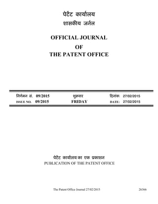
  • 1. The Patent Office Journal 27/02/2015 26366 पेटेंट कायालय शासक य जनल OFFICIAL JOURNAL OF THE PATENT OFFICE िनगमन सं. 09/2015 शुबवार दनांक: 27/02/2015 ISSUE NO. 09/2015 FRIDAY DATE: 27/02/2015 पेटेंट कायालय का एक ूकाशन PUBLICATION OF THE PATENT OFFICE
  • 2. The Patent Office Journal 27/02/2015 26367 INTRODUCTION In view of the recent amendment made in the Patents Act, 1970 by the Patents (Amendment) Act, 2005 effective from 01st January 2005, the Official Journal of The Patent Office is required to be published under the Statute. This Journal is being published on weekly basis on every Friday covering the various proceedings on Patents as required according to the provision of Section 145 of the Patents Act 1970. All the enquiries on this Official Journal and other information as required by the public should be addressed to the Controller General of Patents, Designs & Trade Marks. Suggestions and comments are requested from all quarters so that the content can be enriched. (Chaitanya Prasad) CONTROLLER GENERAL OF PATENTS, DESIGNS & TRADE MARKS 27th FEBRUARY, 2015
  • 3. The Patent Office Journal 27/02/2015 26368 CONTENTS SUBJECT PAGE NUMBER JURISDICTION : 26369 – 26370 SPECIAL NOTICE : 26371 – 26372 EARLY PUBLICATION (DELHI) : 26373 – 26374 EARLY PUBLICATION (MUMBAI) : 26375 – 26388 EARLY PUBLICATION (CHENNAI) : 26389 PUBLICATION AFTER 18 MONTHS (DELHI) : 26390 – 26910 PUBLICATION AFTER 18 MONTHS (MUMBAI) : 26911 – 26912 PUBLICATION AFTER 18 MONTHS (CHENNAI) : 26913 – 27011 PUBLICATION AFTER 18 MONTHS (KOLKATA) : 27012 – 27038 AMENDMENT UNDER SEC. 57 (KOLKATA) : 27039 – 27040 PUBLICATION UNDER SECTION 43(2) IN RESPECT OF THE GRANT (DELHI) : 27041 – 27045 PUBLICATION UNDER SECTION 43(2) IN RESPECT OF THE GRANT (MUMBAI) : 27046 – 27047 PUBLICATION UNDER SECTION 43(2) IN RESPECT OF THE GRANT (CHENNAI) : 27048 – 27049 PUBLICATION UNDER SECTION 43(2) IN RESPECT OF THE GRANT (KOLKATA) : 27050 – 27053 INTRODUCTION TO DESIGN PUBLICATION : 27054 THE DESIGNS ACT 2000 SECTION 30 DESIGN ASSIGNMENT : 27055 CANCELLATION PROCEEDINGS UNDER SECTION 19 OF THE DESIGNS ACT, 2000 : 27056 COPYRIGHT PUBLICATION : 27057 REGISTRATION OF DESIGNS : 27058 - 27115
  • 4. The Patent Office Journal 27/02/2015 26369 THE PATENT OFFICE KOLKATA, 27/02/2015 Address of the Patent Offices/Jurisdictions The following are addresses of all the Patent Offices located at different places having their Territorial Jurisdiction on a Zonal basis as shown below:- 1 Office of the Controller General of Patents, Designs & Trade Marks, Boudhik Sampada Bhavan, Near Antop Hill Post Office,S.M.Road,Antop Hill, Mumbai – 400 037 Phone: (91)(22) 24123311, Fax : (91)(22) 24123322 E-mail: cgpdtm@nic.in 4 The Patent Office, Government of India, Intellectual Property Rights Building, G.S.T. Road, Guindy, Chennai – 600 032. Phone: (91)(44) 2250 2081-84 Fax : (91)(44) 2250 2066 E-mail: chennai-patent@nic.in The States of Andhra Pradesh, Karnataka, Kerala, Tamil Nadu and the Union Territories of Puducherry and Lakshadweep. 2 The Patent Office, Government of India, Boudhik Sampada Bhavan, Near Antop Hill Post Office,S.M.Road,Antop Hill, Mumbai – 400 037 Phone: (91)(22) 24137701 Fax: (91)(22) 24130387 E-mail: mumbai-patent@nic.in The States of Gujarat, Maharashtra, Madhya Pradesh, Goa and Chhattisgarh and the Union Territories of Daman and Diu & Dadra and Nagar Haveli 3 The Patent Office, Government of India, Boudhik Sampada Bhavan, Plot No. 32., Sector-14, Dwarka, New Delhi – 110075 Phone: (91)(11) 2808 1921 – 25 Fax: (91)(11) 2808 1920 & 2808 1940 E.mail: delhi-patent@nic.in The States of Haryana, Himachal Pradesh, Jammu and Kashmir, Punjab, Rajasthan, Uttar Pradesh, Uttaranchal, Delhi and the Union Territory of Chandigarh. 5 The Patent Office (Head Office), Government of India, Boudhik Sampada Bhavan, CP-2, Sector –V, Salt Lake City, Kolkata- 700 091 Phone: (91)(33) 2367 1943/44/45/46/87 Fax: (91)(33) 2367 1988 E-Mail: kolkata-patent@nic.in Rest of India Website: www.ipindia.nic.in www.patentoffice.nic.in All applications, notices, statements or other documents or any fees required by the Patents Act, 1970 and The Patents (Amendment) Act, 2005 or by the Patents (Amendment) Rules, 2006 will be received only at the appropriate offices of the Patent Office. Fees: The Fees may either be paid in cash or may be sent by Bank Draft or Cheques payable to the Controller of Patents drawn on a scheduled Bank at the place where the appropriate office is situated.
  • 5. The Patent Office Journal 27/02/2015 26370 पेटेंट कायालय कोलकाता, दनांक 27/02/2015 कायालय के ेऽािधकार के पतेê विभ न जगह पर ःथत पेटेंट कायालय के पते आंचिलक आधार पर दिशत उनके ूादेिशक अिधकार ेऽ के साथ नीचे दए गए है:- 1 कायालय : महािनयंऽक, एकःव, अिभक प तथा यापार िचहन, एंटोप हल डाकघर के समीप, एस. एम. रोड, एंटोप हल, मु बई- 400 037, भारत, फोन: (91) (22) 24123311 फ़ै स: (91) (22) 24123322 ई. मेल: cgpdtm@nic.in 4 पेटेंट कायालय, भारत सरकार इंटेले चुअल ूॉपट राइ स ब डंग, इंड ःशयल इःटेट एसआईड सीओ आरएमड गोडाउन ए रया एडजसे ट टु ईगल लाःक, जी. एस. ट . रोड, गाय ड चे नई - 600 032. फोन: (91)(44) 2250 2081-84 फ़ै स: (91)(44) 2250-2066 ई. मेल: chennai-patent@nic.in आ ी ूदेश, कनाटक, के रल, तिमलनाडु तथा पुडचेरु रा य ेऽ एवं संघ शािसत ेऽ, ल द प 2 पेटेंट कायालय, भारत सरकार बौ क संपदा भवन, एंटोप हल डाकघर के समीप, एस. एम. रोड, एंटोप हल, मु बई- 400 037, फोन: (91) (22) 24137701 फ़ै स: (91) (22) 24130387 ई. मेल: Mumbai-patent@nic.in गुजरात, महारा , म य ूदेश, गोवा तथा छ ीसगढ़ रा य ेऽ एवं संघ शािसत ेऽ, दमन तथा द व, दादर और नगर हवेली. 3 पेटेंट कायालय, भारत सरकार बौ क संपदा भवन, लॉट सं. 32, से टर- 14, ारका, नई द ली- 110 075. फोन: (91)(11) 2808 1921-25 फ़ै स: (91)(11) 2808 1920, 2808 1940 ई. मेल: delhi-patent@nic.in ह रयाणा, हमाचल ूदेश, ज मू तथा कँमीर, पंजाब,राजःथान, उ र ूदेश, द ली तथा उ रांचल रा य ेऽ , एवं संघ शािसत ेऽ चंड गढ़ 5 पेटेंट कायालय, भारत सरकार कोलकाता, (ूधान कायालय) बौ क संपदा भवन, सीपी-2, से टर- V, सा ट लेक िसट , कोलकाता-700 091, भारत. फोन: (91)(33) 2367 1943/44/45/46/87 फ़ै स:/Fax: (91)(33) 2367 1988 ई. मेल: kolkata-patent@nic.in भारत का अवशेष ेऽ वेबसाइट: http://www.ipindia.nic.in www.patentoffice.nic.in पेटेंट अिधिनयम, 1970 तथा पेटेंट (संशोधन) अिधिनयम, 2005 अथवा पेटेंट (संशोधन) िनयम, 2006 ारा वांिछत सभी आवेदन, सूचनाए, ववरण या अ य दःतावेज़ या कोई शु क पेटेंट कायालय के के वल उपयु कायालय में ःवीकृ त ह गे। शु क: शु क या तो नगद प में या Controller of Patents के नाम में देय बक सा ट या चेक के ारा भेजी जा सकती है जो उसी ःथान के कसी अनुसूिचत बक में ूद हो जहाँ उपयु कायालय ःथत है ।
  • 6. The Patent Office Journal 27/02/2015 26371 SPECIAL NOTICE 18 Months publication as required under Section 11A of the Patents Act, 1970 as amended by the Patents (Amendment) Act, 2005. Notice is hereby given that any person at any time before the grant of Patent may give representation by way of opposition to the Controller of Patents at appropriate office on the ground and in a manner specified under section 25(1) of the Patents (Amendment) Act, 2005 read with Rule 55 of the Patents (Amendment) Rules, 2006. Notice is also given that if any interested person requests for copies of the complete specification, drawing and abstract of any application already published, the photocopy of the same can be supplied by the Patent Office as per the jurisdiction on payment of prescribed fees of Rs.8/- per page. If any further details are required to be obtained, the same can be provided by the respective Patent Offices on request. (Chaitanya Prasad) CONTROLLER GENERAL OF PATENTS, DESIGNS & TRADE MARKS
  • 7. The Patent Office Journal 27/02/2015 26372 SPECIAL NOTICE Under the new provision of the Patents Act, 1970 as amended by the Patents (Amendment) Act, 2005 and Rules there under, Publication of the matter relating to Patents in the Official Gazette of India Part III, Section 2 has been discontinued and instead The Official Journal of the Patent Office is being published containing all the activities of The Patent Office such as publication of all the patent applications after 18th months , grant of patents & all other information in respect of the proceedings as required under the provisions of the Patents (Amendment) Act, 2005 and Rules thereunder on weekly basis on every Friday. The Journal is uploaded in the website every Friday. So Paper form and CD-ROM form of the Journal are discontinued from 01/01/2009. SPECIAL NOTICE Every effort is being taken to publish all the patent applications under section 11(A) of the Patents Act. However, if duplication of publication of any application is found, then earlier date of publication will be taken for the purpose of provisional protection for applicant and Patent Office will grant Patent not before six months from the date of second publication, provided that there is there is no third party representation.
  • 8. The Patent Office Journal 27/02/2015 26373 Early Publication: The following patent applications have been published under section 11A (2) of The Patents (Amendment) Act 2005 and rule 24A of The Patents (Amendment) Rules, 2006. Any person may file representation by way of opposition to the Controller of Patents at the appropriate office against the grant of the patent in the prescribed manner under section 25(1) of the Patents (Amendment) Act 2005 read with the rule 55 of The Patents (Amendment) Rules, 2006: (12) PATENT APPLICATION PUBLICATION (21) Application No.3543/DEL/2014 A (19) INDIA (22) Date of filing of Application :05/12/2014 (43) Publication Date : 27/02/2015 (54) Title of the invention : THE MAGICAL BEND (51) International classification :A01G31/00, A01G31/02 (31) Priority Document No :NA (32) Priority Date :NA (33) Name of priority country :NA (86) International Application No Filing Date :NA :NA (87) International Publication No : NA (61) Patent of Addition to Application Number Filing Date :NA :NA (62) Divisional to Application Number Filing Date :NA :NA (71)Name of Applicant : 1)PANKAJ GURU Address of Applicant :3-61-62, GALI NO.3, NIRANKARI COLONY, DELHI-110 009. Delhi India (72)Name of Inventor : 1)PANKAJ GURU (57) Abstract : The present paper entitled GREEN INTERVENTION is an attempt to analyze the problem of scarce green spaces in the Urban Villages of New Delhi and recommend solutions for the same. With the constant increase in population and the paucity of land, the spaces to live in are significantly decreasing. People are taking every.possible measure to counter the imbalance between abrupt increase in population and the increasing demand for shelter. In an attempt to do so they are creating a huge disparity in the proportion of built and open spaces. No. of Pages : 36 No. of Claims : 6
  • 9. The Patent Office Journal 27/02/2015 26374 (12) PATENT APPLICATION PUBLICATION (21) Application No.4046/DEL/2014 A (19) INDIA (22) Date of filing of Application :31/12/2014 (43) Publication Date : 27/02/2015 (54) Title of the invention : A CORDLESS HAND HELD RF TUBE SEALER. (51) International classification :B65B9/00, H05B6/64 (31) Priority Document No :NA (32) Priority Date :NA (33) Name of priority country :NA (86) International Application No Filing Date :NA :NA (87) International Publication No : NA (61) Patent of Addition to Application Number Filing Date :NA :NA (62) Divisional to Application Number Filing Date :NA :NA (71)Name of Applicant : 1)MAHAJAN; LALIT Address of Applicant :N-118, GREATER KAILASH PART- 1, NEW DELHI, INDIA. Delhi India (72)Name of Inventor : 1)MAHAJAN; LALIT (57) Abstract : The present invention relates to a cordless, handheld, user friendly Radio frequency tube sealer to melt and seal the plastic tubing. It is a Battery supported device so that it is compact in size, user-friendly and ergonomic. The compact, high frequency RF generator (q) is placed within the device which eliminates the use of coaxial cable/cord (c) between the table top RF generator (a) and the handheld tube sealing part (b), so it can be carried to any point of use irrespective of availability of power, is more energy efficient, no RF emission from the co- axial cable to make it safe and it is user-friendly. ,A rechargeable battery ,pack (j) is placed within the device which provides the sufficient current for producing high ,RF energy for the effective uniform melting and sealing of the tube. On activation of the triggerhandle (g), an internal switch is activated and then the RF generator(q) is activated. to transmit the RF energy across the electrodes (o&p) which heats and seals the plastic tubing. No. of Pages : 35 No. of Claims : 7
  • 10. The Patent Office Journal 27/02/2015 26375 (12) PATENT APPLICATION PUBLICATION (21) Application No.3632/MUM/2014 A (19) INDIA (22) Date of filing of Application :18/11/2014 (43) Publication Date : 27/02/2015 (54) Title of the invention : AN IMPROVED MATERIAL UNLOADING DEVICE (51) International classification :D06F 39/00 (31) Priority Document No :NA (32) Priority Date :NA (33) Name of priority country :NA (86) International Application No Filing Date :NA :NA (87) International Publication No : NA (61) Patent of Addition to Application Number Filing Date :NA :NA (62) Divisional to Application Number Filing Date :NA :NA (71)Name of Applicant : 1)L & T MHPS BOILERS PVT. LTD. Address of Applicant :SURAT - HAZIRA ROAD, HAZIRA (WEST), SURAT 394510, GUJARAT, INDIA. (72)Name of Inventor : 1)MR. PANKAJ PATEL 2)MR. KEYUR PAREKH 3)MR. SHAM THAKRE (57) Abstract : An improved material unloading device (1) comprises of the top arm (3) which remains on top of the container (4) comprises of pair of top hook (7) for tying wire rope sling (12) which is directly attached with gantry crane (5) for lifting the material unloading device (l);the said bottom arm (2) which is to be entered inside the container (4) from the backside of the container (4) comprises of the plurality of lug (8) to hold plurality of hook (9) for fastening and lifting the material (6) from the container (4); counter weight (10) is placed which balances unloading device (1) in unloaded condition and stiffeners (11) are provided on side of lower are (2) and upper arm (3) to provide strength to the opening made in the structure. No. of Pages : 12 No. of Claims : 6
  • 11. The Patent Office Journal 27/02/2015 26376 (12) PATENT APPLICATION PUBLICATION (21) Application No.4171/MUM/2014 A (19) INDIA (22) Date of filing of Application :26/12/2014 (43) Publication Date : 27/02/2015 (54) Title of the invention : AN EXPLOSION PROOF ENCLOSURE WITH CAPACITIVE TOUCH INTERFACING SYSTEM (51) International classification :H04B 1/03 (31) Priority Document No :NA (32) Priority Date :NA (33) Name of priority country :NA (86) International Application No Filing Date :NA :NA (87) International Publication No : NA (61) Patent of Addition to Application Number Filing Date :NA :NA (62) Divisional to Application Number Filing Date :NA :NA (71)Name of Applicant : 1)Masibus Automation and Instrumentation Pvt. Ltd. Address of Applicant :B-30,GIDC Electronics Estate, Sector 25, Gandhinagar - 382044, Gujarat, India (72)Name of Inventor : 1)Cordeiro Dominic Joseph 2)Raval Suhant Kirtikumar 3)Haldekar Pankaj Purushottam 4)Mevada Gaurang Bhogilal (57) Abstract : The invention provides an explosion proof container with capacitive touch technology made of explosion proof material includes a main housing (1) and lid (2). The housing (1) has an accommodation place wherein an electronics circuit is disposed. The lid (2) is pivotally connected to the main housing (1) with an LN key operated screw (3). The lid (2) comprises a display circuit board (10) and a capacitive touch sense keyboard (11) disposed on the window glass (9). An electronic circuit disposed within the explosion proof main housing (1) contains SMPS unit (4) and CPU card unit (5). Said CPU card unit (5) contains microcontroller that controls the function of the display board (10) and the capacitive touch keyboard (11). Moreover, the CPU card (5) is also connected to external computer through an industrial communication protocol RS485 for projecting the parameter value of display circuit board (10) on said external computer. No. of Pages : 13 No. of Claims : 6
  • 12. The Patent Office Journal 27/02/2015 26377 (12) PATENT APPLICATION PUBLICATION (21) Application No.3170/MUM/2014 A (19) INDIA (22) Date of filing of Application :07/10/2014 (43) Publication Date : 27/02/2015 (54) Title of the invention : PRECISE LEVEL (51) International classification :G02B27/64 (31) Priority Document No :NA (32) Priority Date :NA (33) Name of priority country :NA (86) International Application No Filing Date :NA :NA (87) International Publication No : NA (61) Patent of Addition to Application Number Filing Date :NA :NA (62) Divisional to Application Number Filing Date :NA :NA (71)Name of Applicant : 1)MR. VAIBHAV SANJAY PAWAR Address of Applicant :A/P:VAHAL, TAL-CHIPLUN, DIST:RATNAGIRI-415641 Maharashtra India (72)Name of Inventor : 1)MR. VAIBHAV SANJAY PAWAR (57) Abstract : A leveling device for measuring, transferring and setting horizontal lines in surveying Disclosed is a leveling device to measure, transfer and set horizontal lines in surveying, the leveling device comprising: a telescope being configured to sight a place to be leveled at desired station and to enable to take staff reading; a level tube being placed above and in parallel to the telescope, the level tube is configured to make axis of the telescope and a line of sight horizontal; a leveling unit being configured to adjust the leveling device to make the line of sight horizontal for any orientation of the telescope; a spindle to hold the telescope and level tube using a level bar, the spindle along with the level bar enables rotational motion of the telescope; a tripod stand for holding the leveling device at a convenient height of the user, the tripod stand comprises tripod head and wings nut arrangement, the tripod stand is fixed to the leveling unit at the tripod head; characterized in that a laser beam generating unit being placed in the wings nut arrangement of tripod stand and configured to generate laser beam and identify exact centre of the leveling device with help of laser beam; the leveling unit comprises three oil spring dampers being fixed on a fixing plate which are interconnecting to each other by pipe network. Under the surface tension phenomenon & property of hydraulic fluid, level the instrument above the spindle to see level; the telescope comprises an eyepiece, a LED light source to be placed in front of the eyepiece, a hair glass having radium measurement markings and an objective glass, the radium measurement markings on the hair glass configured to highlight reading from a staff through the objective glass to ensure accuracy in focusing and to get correct leveling readings. No. of Pages : 23 No. of Claims : 8
  • 13. The Patent Office Journal 27/02/2015 26378 (12) PATENT APPLICATION PUBLICATION (21) Application No.3442/MUM/2014 A (19) INDIA (22) Date of filing of Application :30/10/2014 (43) Publication Date : 27/02/2015 (54) Title of the invention : STEEL LADLE (51) International classification :B04C 9/00 (31) Priority Document No :201420059523.9 (32) Priority Date :02/07/2014 (33) Name of priority country :China (86) International Application No Filing Date :NA :NA (87) International Publication No : NA (61) Patent of Addition to Application Number Filing Date :NA :NA (62) Divisional to Application Number Filing Date :NA :NA (71)Name of Applicant : 1)Puyang Refractories Group Co., Ltd. Address of Applicant :Middle West Circle Road, Puyang County, Henan Province, China (72)Name of Inventor : 1)Peng Dejiang 2)Li Tianqing 3)Gao Jie 4)Lou Junfeng 5)Wang Yonghui 6)Xu Wei 7)Ma Huihui 8)Sun Ronghai 9)Zhang Zhaohai 10)Luo Xingyuan (57) Abstract : The present utility model discloses a steel ladle with a ladle wall that comprises, successively from outside to inside, a ladle case, an insulation layer, a permanent layer and a working layer, wherein the working layer in the slag zone comprises an outer layer and an inner layer which are separate from each other, and the outer layer is located between the inner layer and the permanent layer. The working layer in the slag zone has an overall thickness of D, a thickness of the outer layer of N, and a thickness of the inner layer of M, with N = 10%D-40%D and M = D-N. The present utility model can reduce the waste due to the replacement of the working lining bricks of the steel ladle, reduce the consumption of the refractory material, and therefore lower the cost of steelmaking, and at the same time ensure the safe use of the ladle. No. of Pages : 9 No. of Claims : 9
  • 14. The Patent Office Journal 27/02/2015 26379 (12) PATENT APPLICATION PUBLICATION (21) Application No.430/MUM/2015 A (19) INDIA (22) Date of filing of Application :10/02/2015 (43) Publication Date : 27/02/2015 (54) Title of the invention : SYSTEM FOR ELECTRICAL FAULT DETECTION, INDICATION AND PROTECTION (51) International classification :H04W 24/10 (31) Priority Document No :NA (32) Priority Date :NA (33) Name of priority country :NA (86) International Application No Filing Date :NA :NA (87) International Publication No : NA (61) Patent of Addition to Application Number Filing Date :NA :NA (62) Divisional to Application Number Filing Date :NA :NA (71)Name of Applicant : 1)KAUCHALI ADNAN Address of Applicant :102, AL-AQSA APT, KAUCHALI PATEL MOHALLA, AT POST & TALUKA KHED, DIST. RATNAGIRI - 415 709, MAHARASHTRA, INDIA 2)KALSEKAR DANISH (72)Name of Inventor : 1)KAUCHALI ADNAN 2)KALSEKAR DANISH (57) Abstract : A system for electrical fault detection, indication and protection is disclosed. The system can be used to detect fault conditions in a circuit consisting of 3-phase 3- wire, 3-phase 4-wire, single-phase 2-wire, 2-phase™ 3-wire, and for motor protection. A microcontroller in the system receives sensor output signals, and analyzes the signals with respect to a plurality of trip setting values to determine a fault condition and thereby generate a trip signal, indication of the type of fault and alarm. The system of the present invention is able to distinguish between the different types of fault conditions and act accordingly, can operate over a broad range of load currents, is economical and combines the functions of residual current circuit breaker, arc fault, neutral to ground short, overvoltage, short-circuit, overload, phase drop outs, open neutral, undervoltage, and locked rotor circuit interrupters. No. of Pages : 49 No. of Claims : 12
  • 15. The Patent Office Journal 27/02/2015 26380 (12) PATENT APPLICATION PUBLICATION (21) Application No.159/MUM/2014 A (19) INDIA (22) Date of filing of Application :17/01/2014 (43) Publication Date : 27/02/2015 (54) Title of the invention : VEHICLE DETECTION SYSTEM AND METHOD. (51) International classification :G08G1/01 (31) Priority Document No :NA (32) Priority Date :NA (33) Name of priority country :NA (86) International Application No Filing Date :NA :NA (87) International Publication No : NA (61) Patent of Addition to Application Number Filing Date :NA :NA (62) Divisional to Application Number Filing Date :NA :NA (71)Name of Applicant : 1)KPIT TECHNOLOGIES LTD. Address of Applicant :35 & 36 RAJIV GANDHI INFOTECH PARK, PHASE 1, MIDC, HINJEWADI, PUNE 411057, INDIA Maharashtra India (72)Name of Inventor : 1)GOR SNEHAL 2)BEERUKA, DARSHAN KUMAR (57) Abstract : The present invention describes a vehicle detection system and method for detecting one or more vehicles in a dynamic varying region of interest (ROI). The system comprises a scene recognition module, a road topology estimation module, and a vehicle detecting module. The scene recognition module is configured for receiving either high exposure image or low exposure image for identifying condition of one or more scenes in a dynamically varying region of interest (ROI). The road topology estimation module configured for receiving either high exposure image or low exposure image for determining at least one of a curve, slope and vanishing point of a road in the dynamically varying region of interest (ROI). The vehicle detecting module is coupled with the scene recognition module and road topology module for detecting one or more vehicles on the road at night time. No. of Pages : 62 No. of Claims : 17
  • 16. The Patent Office Journal 27/02/2015 26381 (12) PATENT APPLICATION PUBLICATION (21) Application No.332/MUM/2015 A (19) INDIA (22) Date of filing of Application :02/02/2015 (43) Publication Date : 27/02/2015 (54) Title of the invention : 'KARMANAAV' AN INSTRUMENT FOR DETECTION OF GEOELECTROMAGNETIC FIELD ABOVE GROUND WATER VEIN (51) International classification :G01V 3/08 (31) Priority Document No :NA (32) Priority Date :NA (33) Name of priority country :NA (86) International Application No Filing Date :NA :NA (87) International Publication No : NA (61) Patent of Addition to Application Number Filing Date :NA :NA (62) Divisional to Application Number Filing Date :NA :NA (71)Name of Applicant : 1)NANDKUMAR POPATRAO DHARMADHIKARI Address of Applicant :176/4, HIND COLONY, TRIMURTINAGAR, BHEKRAINAGAR, A/P- PHURSUNGI, TAL-HAVELI, DIST-PUNE (MS) INDIA PIN-412308 Maharashtra India (72)Name of Inventor : 1)NANDKUMAR POPATRAO DHARMADHIKARI 2)AVINASH G. KHARAT 3)CHANDRAKANT SHANKAR MAHAJAN 4)MADHUKAR SANTOSH PATIL 5)AISHWARYA BHIMRAJ GAWAND 6)RAVIRAJ RAMESH SORATE (57) Abstract : an instrument for detection of geoelectromagnetic field above ground water vein in a built environment is invented. It consists of enclosed wooden box having plane polarized light and photodiode as detector. It also consists of angle measuring device to measure rotation of plane polarization. This instrument has been invented to further confirm the presence of ground water vein detected by dowsing and also to aid calculation of depth and flow of water. No. of Pages : 6 No. of Claims : 3
  • 17. The Patent Office Journal 27/02/2015 26382 (12) PATENT APPLICATION PUBLICATION (21) Application No.3936/MUM/2014 A (19) INDIA (22) Date of filing of Application :09/12/2014 (43) Publication Date : 27/02/2015 (54) Title of the invention : A PROCESS RELATED TO SYSTEMS AND METHODS FOR PROVIDING CUSTOMIZED SOLUTION FOR FURNITURE (51) International classification :B44C 3/12 (31) Priority Document No :NA (32) Priority Date :NA (33) Name of priority country :NA (86) International Application No Filing Date :NA :NA (87) International Publication No : NA (61) Patent of Addition to Application Number Filing Date :NA :NA (62) Divisional to Application Number Filing Date :NA :NA (71)Name of Applicant : 1)MR. GAURAV AGARWAL Address of Applicant :MHATRE PEN BUILDING, 'A' WING, 2ND FLOOR, S. B. MARG, DADAR (WEST), MUMBAI-400 028 Maharashtra India (72)Name of Inventor : 1)MR. GAURAV AGARWAL (57) Abstract : A process related to systems and methods for providing customized solution for furniture by combining the features of readymade furniture and completely knock down furniture by describing the parameters relates to:- i) Materials to be used. j) Size of board to be used k) Internal arrangement 1) Financial of the size of final items m) Customization according to the space available. n) Surface finish and colour. o) Final product p) Installation No. of Pages : 30 No. of Claims : 4
  • 18. The Patent Office Journal 27/02/2015 26383 (12) PATENT APPLICATION PUBLICATION (21) Application No.394/MUM/2014 A (19) INDIA (22) Date of filing of Application :04/02/2014 (43) Publication Date : 27/02/2015 (54) Title of the invention : COMPOSITION FOR RELIEVING PAIN, STRESS AND INSOMNIA (51) International classification :A61K6/00, A61K8/97, A61K36/76, A61K36 (31) Priority Document No :NA (32) Priority Date :NA (33) Name of priority country :NA (86) International Application No Filing Date :NA :NA (87) International Publication No : NA (61) Patent of Addition to Application Number Filing Date :NA :NA (62) Divisional to Application Number Filing Date :NA :NA (71)Name of Applicant : 1)Ashvany Kumar Bansal Address of Applicant :K-3, 27 & 28, Spaghetti CHSL, Sector- 15, Kharghar, Navi Mumbai-410210, Maharashtra, India (72)Name of Inventor : 1)Ashvany Kumar Bansal (57) Abstract : The present invention relates to a composition for relieving one or more of the conditions of pain, stress and insomnia comprising Brassica compestris, Bees wax and Dryobalanops camphora. The present invention also provides a formulation comprising the composition of the present invention as well as method for preparation thereof, uses thereof and method of treatment of one or more of the conditions of pain, stress and insomnia. No. of Pages : 36 No. of Claims : 14
  • 19. The Patent Office Journal 27/02/2015 26384 (12) PATENT APPLICATION PUBLICATION (21) Application No.3940/MUM/2014 A (19) INDIA (22) Date of filing of Application :09/12/2014 (43) Publication Date : 27/02/2015 (54) Title of the invention : A RAIL-TRACK SWITCHING SYSTEM FOR SWITCHING TRACK OF A RAIL GUIDED VEHICLE (51) International classification :B60M 7/00 (31) Priority Document No :NA (32) Priority Date :NA (33) Name of priority country :NA (86) International Application No Filing Date :NA :NA (87) International Publication No : NA (61) Patent of Addition to Application Number Filing Date :NA :NA (62) Divisional to Application Number Filing Date :NA :NA (71)Name of Applicant : 1)KONKAN RAILWAY CORPORATION LIMITED Address of Applicant :Belapur Bhavan, Sector 11, CBD Belapur, Navi Mumbai - 400614, Maharashtra, India (72)Name of Inventor : 1)BHATT AJAYKUMAR AMARNATH 2)LINGAIAH PRAKASH (57) Abstract : A rail-track switching system for switching rail guided vehicle from a first track to a second track, the rail-track switching system comprising a pair of stock rails fixed on a base, a pair of tongue rails slidably disposed between the pair of stock rails, a leading stretcher bar that is disposed between the pair of tongue rails and provided with a pair of clamping elements configured on an end portions of the leading stretcher bar for clamping the leading stretcher bar, and at least one following stretcher bar that comprises a pair of stretcher elements functionally coupled to each other and the tongue rails and adapted to move collectively together and independently relative to each other to change the longitudinal dimension of the following stretcher bar. No. of Pages : 25 No. of Claims : 5
  • 20. The Patent Office Journal 27/02/2015 26385 (12) PATENT APPLICATION PUBLICATION (21) Application No.4229/MUM/2014 A (19) INDIA (22) Date of filing of Application :30/12/2014 (43) Publication Date : 27/02/2015 (54) Title of the invention : AN ARRANGEMENT AND METHOD FOR REDUCING THE WEAR OF ROTOR AND ITS PARTS. (51) International classification :H01H 33/16 (31) Priority Document No :NA (32) Priority Date :NA (33) Name of priority country :NA (86) International Application No Filing Date :NA :NA (87) International Publication No : NA (61) Patent of Addition to Application Number Filing Date :NA :NA (62) Divisional to Application Number Filing Date :NA :NA (71)Name of Applicant : 1)Kalani Jugal Kishore Kunjilal Address of Applicant :H-2, Old M.I.D.C., Satara Maharashtra India (72)Name of Inventor : 1)Kalani Jugal Kishore Kunjilal (57) Abstract : A vertical shaft impact (VSI) crusher with a rotor (2) mounted on a shaft for accelerating flow of material to be crushed in a crushing chamber (7), a feed tube (3) through which the material to be crushed is passed vertically downwards into the rotor(2);a distribution plate (4) fixed rigidly at centre of the rotor (2) which, enables distribution of the material along circumference of the rotor(2); the feed tube (3) being placed at a predetermined height above the distribution plate (4) to allow the material to fall gently on the distribution plate (4); and an armor cone (5) covering the rotor for avoiding falling of rebounded crushed material on the rotor(2) and an armor ring (6) is provided to prevent wear of the rotor(2) . The invention also provides for a method of reducing the wear of a rotor. No. of Pages : 15 No. of Claims : 8
  • 21. The Patent Office Journal 27/02/2015 26386 (12) PATENT APPLICATION PUBLICATION (21) Application No.357/MUM/2015 A (19) INDIA (22) Date of filing of Application :03/02/2015 (43) Publication Date : 27/02/2015 (54) Title of the invention : INNOVATIVE LARGE SCALE PRODUCTION OF COST EFFECTIVE SANITARY PAD FOR HYGIENE OF RURAL WOMEN (51) International classification :A61F 13/15 (31) Priority Document No :NA (32) Priority Date :NA (33) Name of priority country :NA (86) International Application No Filing Date :NA :NA (87) International Publication No : NA (61) Patent of Addition to Application Number Filing Date :NA :NA (62) Divisional to Application Number Filing Date :NA :NA (71)Name of Applicant : 1)MISS PRUTHA PRASHANT JOSHI Address of Applicant :A-2/2, SIDDHANT, JAYSHREE CO- OP SOCIETY, KATHE LANE, DWARKA, NASHIK-422011, MAHARASHTRA, INDIA. 2)MISS AALOKA S. KOTWAL 3)MR. PRATHAMESH H. BORKAR (72)Name of Inventor : 1)MISS PRUTHA PRASHANT JOSHI 2)MISS AALOKA S. KOTWAL 3)MR. PRATHAMESH H. BORKAR (57) Abstract : Menstrual hygiene management is a big problem for women in villages as the sanitary pads are expensive. An average pack of 8 is significantly expensive for females coming from low income families, which has caused women and girls to resort to unhealthy ways such as using grass and cow dung for managing their menstruation, which exposes them to infections. The design was based on the substitution of core material used for making of conventional sanitary pads with more absorbent jute linters which otherwise is regarded as waste. To resolve the infection problem with bacteria during the menstruation, the core layer is padded with aloevera (which is inherently antibacterial). In our invention, an attempt has been made to design low cost sanitary napkins by utilizing maximum benefit out of regular cheaper products. The process has been described for the large scale production of 1000 packets (8 pads per pack) per day. No. of Pages : 13 No. of Claims : 5
  • 22. The Patent Office Journal 27/02/2015 26387 (12) PATENT APPLICATION PUBLICATION (21) Application No.37/MUM/2014 A (19) INDIA (22) Date of filing of Application :06/01/2014 (43) Publication Date : 27/02/2015 (54) Title of the invention : A METHOD AND A SYSTEM THEREOF FOR PROVIDING CLOSE TO ZERO REACTIVE POWER PASSIVE CURRENT HARMONIC FILTER FOR NON-LINEAR LOADS (51) International classification :H02J3/01, Y02E40/40 (31) Priority Document No :NA (32) Priority Date :NA (33) Name of priority country :NA (86) International Application No Filing Date :NA :NA (87) International Publication No : NA (61) Patent of Addition to Application Number Filing Date :NA :NA (62) Divisional to Application Number Filing Date :NA :NA (71)Name of Applicant : 1)Shreem Electric Limited Address of Applicant :Plot No. 43-46, L. K. Akiwate Industrial Estate, Jaysingpur (Dist. Kolhapur) , MH India Maharashtra India (72)Name of Inventor : 1)Vilas Rajaram Kanetkar 2)Kumar Eknath Shinde (57) Abstract : The present invention provides a method and a system thereof for providing Zero Reactive Power Passive Current Harmonic Filter (ZRPPCHF) for a non-linear load. The method and the system thereof having steps of identifying supply voltage and frequency. Thereafter, obtaining Short Circuit Capacity and hence a Short Circuit Inductance of an electric supply at the point of PCC (Point of Common Coupling), and details of non-linear load which includes VA/kVA, Watts/kW, VAr/kVAr and current harmonics produced by the non-linear load. Further, identifying Short Circuit Current to Rated Load Current Ratio (SCR). Then identifying specified current harmonic and voltage harmonic distortion of the electric supply. Thereafter, deriving filter error impedance to achieve specified current harmonic distortion. Further, configuring a filter system in parallel with the non-linear load for absorbing current harmonics from the non-linear load, wherein the difference between nth harmonic filter impedance error is 1/20th of that of Short Circuit Impedance for the nth harmonic. At last, configuring an additional very low frequency parallel filter (Li and Ci) to compensate fundamental capacitive reactive power absorbed by the filter system configured for absorbing non-linear load current harmonics. No. of Pages : 50 No. of Claims : 4
  • 23. The Patent Office Journal 27/02/2015 26388 (12) PATENT APPLICATION PUBLICATION (21) Application No.2040/MUM/2014 A (19) INDIA (22) Date of filing of Application :25/06/2014 (43) Publication Date : 27/02/2015 (54) Title of the invention : EMG BASED WIRELESS ASSISTIVE PORTABLE 3 FINGER ROBOTIC HAND (51) International classification :H05B 37/02 (31) Priority Document No :NA (32) Priority Date :NA (33) Name of priority country :NA (86) International Application No Filing Date :NA :NA (87) International Publication No : NA (61) Patent of Addition to Application Number Filing Date :NA :NA (62) Divisional to Application Number Filing Date :NA :NA (71)Name of Applicant : 1)Sumit Arun Raurale Address of Applicant :10, Forest ColonyNear Yashoda Nagar, Old Bye Pass Road, Amravati-444606 Maharashtra India (72)Name of Inventor : 1)Sumit Arun Raurale (57) Abstract : Present invention provides specially a portable device that feasibly assist the robotic hand prosthesis movement™s like opening and closing of hand, extension and flexion of wrist, extension and flexion of elbow; which offers more mobility to the disabled hand persons without the need of complex array of sensing electrodes, mathematical transformation and computer processing. So to increase the effectiveness of hand prostheses, it consider the surface myoelectric (EMG) signals which are further used as a control signal of the human active hand movements for assistive robotic hand. For daily living hand activity, we use only the three fingers viz. the thumb, index and middle finger for maximum working tasks, so we have built the three fingers prosthesis controlled robotic hand. In this, we have developed a wireless prosthesis robotic hand movements which can be operated in real time assessment with high accuracy. Also for developing a portable and economical model, only three electrodes are been used for acquisition of EMG signal and the EMG signal processing is done with the ATmega16 controller which has removed the computer module from the system and make our system a compact, portable and cost efficient system. Following invention is described in detail with the help of Figure 1 of sheet 1 showing the schematic block diagram of the present invention. No. of Pages : 22 No. of Claims : 8
  • 24. The Patent Office Journal 27/02/2015 26389 (12) PATENT APPLICATION PUBLICATION (21) Application No.187/KOL/2015 A (19) INDIA (22) Date of filing of Application :17/02/2015 (43) Publication Date : 27/02/2015 (54) Title of the invention : NEURAL NETWORK BASED HIGH SPEED COMPOUND IMAGE COMPRESSION SYSTEM BASED ON DWT COEFFICIENTS (51) International classification :G06T7/40 (31) Priority Document No :NA (32) Priority Date :NA (33) Name of priority country :NA (86) International Application No Filing Date :NA :NA (87) International Publication No : NA (61) Patent of Addition to Application Number Filing Date :NA :NA (62) Divisional to Application Number Filing Date :NA :NA (71)Name of Applicant : 1)PROF. (DR.) JAGADEESH KUMAR Address of Applicant :JIS COLLEGE OF ENGINEERING, KALYANI, NADIA - 741235, WEST BENGAL, INDIA. 2)INDRANIL SARKAR 3)SUKANYA BANERJEE (72)Name of Inventor : 1)PROF. (DR.) JAGADEESH KUMAR (57) Abstract : This invention relates to a neural network based high speed compound Image compression systemand in particular, this invention relates to the neural network based high speed compound Image compression system based on DWT coefficients. More particularly, this present invention also relates to neural network based high speed compound Image compression systemto maximize the precision and recall rate of the classification algorithm, while at the same time minimizing the execution and training time of the neural network. No. of Pages : 15 No. of Claims : 7
  • 25. The Patent Office Journal 27/02/2015 26390 Publication After 18 Months: The following Patent Applications have been published under Section 11A (3) of The Patents (Amendment) Act, 2005. Any Person may file representation by way of opposition to the Controller of Patents at the appropriate office against the grant of the patent in the prescribed manner under section 25(1) of the Patents (Amendment) Act, 2005 read with the rule 55 of The Patents (Amendment) Rules, 2006: (12) PATENT APPLICATION PUBLICATION (21) Application No.11/DEL/2014 A (19) INDIA (22) Date of filing of Application :03/01/2014 (43) Publication Date : 27/02/2015 (54) Title of the invention : METHOD FOR PREPARING CELLULOSE ETHER HAVING LOW DEGREE OF POLYMERIZATION AND CELLULOSE ETHER PREPARED THEREBY (51) International classification :C08B (31) Priority Document No :2013- 002076 (32) Priority Date :09/01/2013 (33) Name of priority country :Japan (86) International Application No Filing Date :NA :NA (87) International Publication No : NA (61) Patent of Addition to Application Number Filing Date :NA :NA (62) Divisional to Application Number Filing Date :NA :NA (71)Name of Applicant : 1)SHIN-ETSU CHEMICAL CO., LTD. Address of Applicant :6-1, Otemachi 2-chome, Chiyoda-ku, Tokyo, JAPAN (72)Name of Inventor : 1)NARITA, Mitsuo 2)NISHIYAMA, Yuichi (57) Abstract : Provided are a method for preparing a cellulose ether having a low degree of polymerization and undergoing less yellowing and a cellulose ether prepared thereby. More specifically, provided is a method for preparing a cellulose ether having a low degree of polymerization, the method comprising a step of bringing pulp and an alkali metal hydroxide solution into contact with each other or mixing them to obtain a corresponding alkali cellulose, a first depolymerization step of reacting the alkali cellulose with oxygen to adjust a viscosity reduction percentage of the alkali cellulose to from 10 to 95%, a step of reacting the depolymerized alkali cellulose with an etherifying agent, a step of washing and drying the reaction product to obtain a cellulose ether, and a second depolymerization step of bringing the cellulose ether into contact with hydrochloric acid to adjust a viscosity reduction percentage of the cellulose ether to from 40 to 99.9%. No. of Pages : 25 No. of Claims : 4
  • 26. The Patent Office Journal 27/02/2015 26391 (12) PATENT APPLICATION PUBLICATION (21) Application No.2475/DEL/2013 A (19) INDIA (22) Date of filing of Application :22/08/2013 (43) Publication Date : 27/02/2015 (54) Title of the invention : A NOVEL FLY ASH BASED ZEOLITIC EXTENDER PIGMENT FOR USE AS ANTI-CORROSIVE ADDITIVE IN PAINTS (51) International classification :C04B (31) Priority Document No :NA (32) Priority Date :NA (33) Name of priority country :NA (86) International Application No Filing Date :NA :NA (87) International Publication No : NA (61) Patent of Addition to Application Number Filing Date :NA :NA (62) Divisional to Application Number Filing Date :NA :NA (71)Name of Applicant : 1)AMITY UNIVERSITY Address of Applicant :AMITY UNIVERSITY CAMPUS, SECTOR-125, NOIDA-201303, UP, INDIA Uttar Pradesh India (72)Name of Inventor : 1)SANGEETA TIWARI (57) Abstract : The present invention relates to a novel modified zeolitic extender pigment from industrial waste that can be used in anticorrosive paints. Fly ash, an industrial waste from thermal power stations has been modified by alkali fusion followed by hydrothertmal treatment to obtain a nanosized mesoporous material. Metal ions specific for corrosion protection were incorporated in its structure. The modified fly ash based material when used in paints as an extender, exhibited significant anticorrosive properties. No. of Pages : 14 No. of Claims : 8
  • 27. The Patent Office Journal 27/02/2015 26392 (12) PATENT APPLICATION PUBLICATION (21) Application No.2581/DELNP/2014 A (19) INDIA (22) Date of filing of Application :02/04/2014 (43) Publication Date : 27/02/2015 (54) Title of the invention : NANOPARTICLE TUMOUR VACCINES (51) International classification :A61K47/48,A61P35/00 (31) Priority Document No :61/531730 (32) Priority Date :07/09/2011 (33) Name of priority country :U.S.A. (86) International Application No Filing Date :PCT/EP2012/067579 :07/09/2012 (87) International Publication No :WO 2013/034741 (61) Patent of Addition to Application Number Filing Date :NA :NA (62) Divisional to Application Number Filing Date :NA :NA (71)Name of Applicant : 1)MIDATECH LIMITED Address of Applicant :4 & 5 Dunmore Court Wootton Road Abingdon Oxford Oxfordshire OX13 6BH U.K. 2)IMMUNOTOPE INC. (72)Name of Inventor : 1)RADEMACHER Thomas 2)PHILIP Ramila (57) Abstract : THE PRESENT INVENTION PROVIDES A VACCINE FOR THE PROPHYLACTIC OR THERAPEUTIC TREATMENT OF A TUMOUR IN A MAMMALIAN SUBJECT AS WELL AS METHODS OF USING THE VACCINE INCLUDING IN TREATMENT OF TUMOURS AND IN GENERATING A CTL RESPONSE. THE VACCINE COMPRISES A PLURALITY OF NANOPARTICLES AND A PHARMACEUTICALLY ACCEPTABLE CARRIER SALT OR DILUENT. THE NANOPARTICLES COMPRISE A CORE COMPRISING A METAL AND/OR A SEMICONDUCTOR ATOM; AND A CORONA COMPRISING A PLURALITY OF LIGANDS COVALENTLY LINKED TO THE CORE WHEREIN AT LEAST A FIRST LIGAND OF SAID PLURALITY COMPRISES A CARBOHYDRATE MOIETY THAT IS COVALENTLY LINKED TO THE CORE VIA A FIRST LINKER AND WHEREIN AT LEAST A SECOND LIGAND OF SAID PLURALITY COMPRISES AN EPITOPIC PEPTIDE THAT IS COVALENTLY LINKED TO THE CORE VIA A SECOND LINKER SAID SECOND LINKER COMPRISING A PEPTIDE PORTION AND A NON PEPTIDE PORTION WHEREIN SAID PEPTIDE PORTION COMPRISES THE SEQUENCE XXZ WHEREIN: X IS AN AMINO ACID SELECTED FROM A AND G; X IS AN AMINO ACID SELECTED FROM A AND G; AND Z IS AN AMINO ACID SELECTED FROM Y AND F AND WHEREIN SAID EPITOPIC PEPTIDE FORMS AT LEAST A PORTION OF OR IS DERIVED FROM A TUMOUR ASSOCIATED ANTIGEN (TAA). No. of Pages : 100 No. of Claims : 63
  • 28. The Patent Office Journal 27/02/2015 26393 (12) PATENT APPLICATION PUBLICATION (21) Application No.2642/DELNP/2014 A (19) INDIA (22) Date of filing of Application :03/04/2014 (43) Publication Date : 27/02/2015 (54) Title of the invention : MANAGEMENT AND ASSISTANCE SYSTEM FOR THE DEAF (51) International classification :G10L21/00, G10L11/00, G10L21/06 (31) Priority Document No :11/041,166 (32) Priority Date :21/01/2005 (33) Name of priority country :U.S.A. (86) International Application No Filing Date :PCT/US2005/046246 :20/12/2005 (87) International Publication No : NA (61) Patent of Addition to Application Number Filing Date :NA :NA (62) Divisional to Application Number Filed on :5254/DELNP/2007 :06/07/2007 (71)Name of Applicant : 1)KATES, Lawrence Address of Applicant :1111 Bayside Drive, Corona Del Mar, California 92625, U.S.A. (72)Name of Inventor : 1)KATES, Lawrence (57) Abstract : A computer-aided communication and assistance system that uses a signal processing and other algorithms in a processor in wireless communication with a microphone system to aid a deaf person. An instrumented communication module receives information from one or more microphones and provides textual and, optionally, stimulatory information to the deaf person. In one embodiment, a microphone is provided in a piece of jewelry or clothing. In one embodiment, a wireless (or wired) earpiece is provided to provide microphones and vibration stimulators. No. of Pages : 34 No. of Claims : 20
  • 29. The Patent Office Journal 27/02/2015 26394 (12) PATENT APPLICATION PUBLICATION (21) Application No.118/DEL/2014 A (19) INDIA (22) Date of filing of Application :15/01/2014 (43) Publication Date : 27/02/2015 (54) Title of the invention : VEHICULAR AIR CONDITIONER CONTROL DEVICE (51) International classification :F16H (31) Priority Document No :2013- 005125 (32) Priority Date :16/01/2013 (33) Name of priority country :Japan (86) International Application No Filing Date :NA :NA (87) International Publication No : NA (61) Patent of Addition to Application Number Filing Date :NA :NA (62) Divisional to Application Number Filing Date :NA :NA (71)Name of Applicant : 1)Suzuki Motor Corporation Address of Applicant :300, Takatsuka-cho, Minami-ku, Hamamatsu-shi, Shizuoka 432-8611 (JP) Japan (72)Name of Inventor : 1)MATSUMOTO, Kei 2)SHIBATA, Koichi (57) Abstract : There is provided a vehicular air conditioner control device. Creep torque generation means is configured to generate driving torque for moving a vehicle even when an internal combustion engine is at an idling state. An air conditioner is configured to be driven with using power generated from the internal combustion engine. Air conditioner control means is configured to control an operating state of the air conditioner. Brake negative pressure detection means is configured to detect a negative pressure amount of a brake. The air conditioner control means stops the air conditioner when the brake negative pressure amount detected by the brake negative pressure detection means is lower than a predetermined value and the driving torque is generated by the creep torque generation means to start moving the vehicle by the generated driving torque. No. of Pages : 19 No. of Claims : 2
  • 30. The Patent Office Journal 27/02/2015 26395 (12) PATENT APPLICATION PUBLICATION (21) Application No.2484/DEL/2013 A (19) INDIA (22) Date of filing of Application :22/08/2013 (43) Publication Date : 27/02/2015 (54) Title of the invention : METHOD AND APPARATUS FOR INTRODUCING LONGER PAGING CYCLES IN A CELLULAR NETWORK (51) International classification :H04W (31) Priority Document No :NA (32) Priority Date :NA (33) Name of priority country :NA (86) International Application No Filing Date :NA :NA (87) International Publication No : NA (61) Patent of Addition to Application Number Filing Date :NA :NA (62) Divisional to Application Number Filing Date :NA :NA (71)Name of Applicant : 1)Telefonaktiebolaget LM Ericsson (Publ) Address of Applicant :SE-164 83 Stockholm (SE) Sweden (72)Name of Inventor : 1)SCHLIWA-BERTLING, Paul 2)BALLAKUR, Ravitej 3)DAS, Sajal Kumar 4)DIACHINA, John Walter 5)SUNDBERG, Mrten (57) Abstract : The present invention relates to a method and apparatus to reduce power usage in a terminal or mobile station (MS), comprising performing wake-up and synchronization operations according to a long DRX period. No. of Pages : 13 No. of Claims : 7
  • 31. The Patent Office Journal 27/02/2015 26396 (12) PATENT APPLICATION PUBLICATION (21) Application No.2485/DEL/2013 A (19) INDIA (22) Date of filing of Application :23/08/2013 (43) Publication Date : 27/02/2015 (54) Title of the invention : MEDIA FOR IN VITRO DISSOLUTION TESTING OF POLYSACCHARIDE BASED COLON TARGETED FORMULATIONS AND METHOD THEREOF (51) International classification :A61K (31) Priority Document No :NA (32) Priority Date :NA (33) Name of priority country :NA (86) International Application No Filing Date :NA :NA (87) International Publication No : NA (61) Patent of Addition to Application Number Filing Date :NA :NA (62) Divisional to Application Number Filing Date :NA :NA (71)Name of Applicant : 1)MITTAL AMAN Address of Applicant :Deputy Director Lovely Professional University (LPU) Phagwara-144411 PUNJAB India (72)Name of Inventor : 1)Goud Niranjan Kotla 2)Gulati Monica 3)Singh Sachin Kumar 4)Basotra Mohit 5)Chaudhary Yashwant (57) Abstract : The present invention discloses a novel, probiotic based dissolution media for in vitro testing of drug release from colon specific polysaccharide based formulations comprising a mixture of nutrition sources and specific polysaccharide digesting microbe(s) added externally. During testing, buffering salts are added to the media. In a preferred embodiment, the invention comprises 5 % w/v of Grade A honey, 12 % w/v reconstituted nonfat dry milk power (NDM) and 2 % w/v of the probiotics Bifidobacterium longum, Bifidobacterium bifidum (0.24 billion CFU or colony forming units each) and Sachharomyces boulardi (0.05 billion CFU) in sterile water to which buffering salts are added during testing. Release profile in media of present invention is similar to that obtained using media containing rat cecal contents. The invention thus offers a reliable and economical method for testing of colon specific polysaccharide based formulations, without sacrifice of animals. No. of Pages : 22 No. of Claims : 4
  • 32. The Patent Office Journal 27/02/2015 26397 (12) PATENT APPLICATION PUBLICATION (21) Application No.2643/DELNP/2014 A (19) INDIA (22) Date of filing of Application :03/04/2014 (43) Publication Date : 27/02/2015 (54) Title of the invention : NOVEL COMPOSITION FOR PREPARING POLYSACCHARIDE FIBERS (51) International classification :D01F9/00,C08L5/00 (31) Priority Document No :61/543423 (32) Priority Date :05/10/2011 (33) Name of priority country :U.S.A. (86) International Application No Filing Date :PCT/US2012/058850 :05/10/2012 (87) International Publication No :WO 2013/052730 (61) Patent of Addition to Application Number Filing Date :NA :NA (62) Divisional to Application Number Filing Date :NA :NA (71)Name of Applicant : 1)E. I. DU PONT DE NEMOURS AND COMPANY Address of Applicant :1007 Market Street Wilmington DE 19899 U.S.A. (72)Name of Inventor : 1)OBRIEN John P. 2)OPPER Kathleen (57) Abstract : THIS INVENTION PERTAINS TO A NOVEL PROCESS FOR PREPARING FIBERS FROM POLY(A(1,3) GLUCAN). THE FIBERS PREPARED ACCORDING TO THE INVENTION HAVECOTTON LIKE PROPERTIES ARE USEFUL IN TEXTILE APPLICATIONS AND CAN BE PRODUCED AS CONTINUOUS FILAMENTS ON A YEAR ROUND BASIS. THE PROCESS COMPRISES SOLUTION SPINNING FROM A NOVEL SOLUTION OF POLY(A(1,3) GLUCAN) IN A MIXTURE OF WATER AND N METHYLMORPHOLINE N OXIDE FOLLOWED BY COAGULATION IN A LIQUID COAGULANT THAT COMPRISES A LIQUID THAT IS NOT WATER. No. of Pages : 43 No. of Claims : 14
  • 33. The Patent Office Journal 27/02/2015 26398 (12) PATENT APPLICATION PUBLICATION (21) Application No.2645/DELNP/2014 A (19) INDIA (22) Date of filing of Application :03/04/2014 (43) Publication Date : 27/02/2015 (54) Title of the invention : A STEAM METHANE REFORMING METHOD (51) International classification :C01B3/00 (31) Priority Document No :10/990,485 (32) Priority Date :18/11/2004 (33) Name of priority country :U.S.A. (86) International Application No Filing Date :PCT/US2005/040336 :07/11/2005 (87) International Publication No : NA (61) Patent of Addition to Application Number Filing Date :NA :NA (62) Divisional to Application Number Filed on :3456/DELNP/2007 :09/05/2007 (71)Name of Applicant : 1)PRAXAIR TECHNOLOGY, INC., Address of Applicant :39 Old Ridgebury Road, Danbury, State of Connecticut 06810-5113, United States of America, (72)Name of Inventor : 1)RAYMOND FRANCIS DRNEVICH 2)VASIIS PAPAVASSILIOU (57) Abstract : A steam methane reforming method comprising: heating a feed stream comprising hydrocarbons, sulfur compounds and hydrogen to a temperature of no greater than 600 C; producing an intermediate product stream by catalytically reacting said hydrogen with the hydrocarbons and the sulfur compounds without oxygen so that the intermediate product stream contains saturated hydrocarbons and hydrogen sulfidc formed from hydrogenation of the hydrocarbons and the sulfur compounds, respectively, the heating of the feed stream and/or the hydrogenation of the hydrocarbons being sufficient to produce the intermediate product stream at a temperature of greater than 400 C or alternatively, catalytically reacting oxygen, steam and the hydrocarbons, the hydrogen and the sulfur compounds contained within the feed stream so that the intermediate product stream contains additional hydrogen and carbon monoxide produced by reaction of the oxygen, steam and hydrocarbons and hydrogen sulfide produced by conversion of the sulfur compounds, the oxygen being present in a sufficient amount that the intermediate produced stream is produced at a temperature of between 500 C and 860 C and at steam to carbon and oxygen to carbon ratios being selected to control an amount of moles of the additional hydrogen produced and at less than 0.5 and less than 0.25, respectively; No. of Pages : 46 No. of Claims : 12
  • 34. The Patent Office Journal 27/02/2015 26399 (12) PATENT APPLICATION PUBLICATION (21) Application No.2465/DEL/2013 A (19) INDIA (22) Date of filing of Application :21/08/2013 (43) Publication Date : 27/02/2015 (54) Title of the invention : TUNABLE LED BASED ELECTROPHORESIS COUPLED GEL DOCUMENTATION SYSTEM (51) International classification :G01N (31) Priority Document No :NA (32) Priority Date :NA (33) Name of priority country :NA (86) International Application No Filing Date :NA :NA (87) International Publication No : NA (61) Patent of Addition to Application Number Filing Date :NA :NA (62) Divisional to Application Number Filing Date :NA :NA (71)Name of Applicant : 1)BHARDWAJ SANJEEV KUMAR Address of Applicant :AD-23, HMT Colony, PINJORE - 134101 Distt. Panchkula Haryana INDIA 2)NEHA (72)Name of Inventor : 1)BHARDWAJ SANJEEV KUMAR 2)NEHA 3)DAHIYA SWATI 4)TRIPATHI CHANDRA CHARU (57) Abstract : The present invention discloses a real-time observable electrophoresis coupled gel-doc system in which visualization of samples using different dyes is possible within the same system, owing to presence of a tunable LED, which emits nearly monochromatic light adjusted to absorption frequency of dyes by appropriately controlling the supply voltage. The invention minimizes the noise and hence improved band visualization due to fine tuning of the wavelength of excitation source for visualization of DNA/RNA and protein bands in contrast to broad source employed in prior art system. Different dyes can be used using a single electrophoresis system, since the excitation source is tunable. By use of image processing /enhancement algorithm which includes background subtraction, contrast enhancement, edge detection and segmentation DNA band can easily be enhanced. No. of Pages : 17 No. of Claims : 7
  • 35. The Patent Office Journal 27/02/2015 26400 (12) PATENT APPLICATION PUBLICATION (21) Application No.2737/DELNP/2014 A (19) INDIA (22) Date of filing of Application :04/04/2014 (43) Publication Date : 27/02/2015 (54) Title of the invention : EXCHANGEABLE LENS (51) International classification :G03B17/14,H04N5/225 (31) Priority Document No :2011198422 (32) Priority Date :12/09/2011 (33) Name of priority country :Japan (86) International Application No Filing Date :PCT/JP2012/073372 :12/09/2012 (87) International Publication No :WO 2013/039120 (61) Patent of Addition to Application Number Filing Date :NA :NA (62) Divisional to Application Number Filing Date :NA :NA (71)Name of Applicant : 1)NIKON CORPORATION Address of Applicant :12 1 Yurakucho 1 chome Chiyoda ku Tokyo 1008331 Japan (72)Name of Inventor : 1)IMAFUJI Kazuharu (57) Abstract : An exchangeable lens is provided with: an attachment part capable of attaching to a camera body; a photographing optical system including a plurality of driven members for which the state of being driven changes; a driven information transmission unit for transmitting multiple driven information items pertaining to the location of the plurality of driven members to the camera body according to a clock signal outputted by the camera body; and a type information transmission unit for transmitting type information via a first transmission unit that represents the type of driven information that the driven information transmission unit is capable of transmitting. Therein the driven information transmission unit transmits driven information for each of the plurality of driven members via a first transmission unit or a second transmission unit differing therefrom. No. of Pages : 40 No. of Claims : 5
  • 36. The Patent Office Journal 27/02/2015 26401 (12) PATENT APPLICATION PUBLICATION (21) Application No.2738/DELNP/2014 A (19) INDIA (22) Date of filing of Application :07/04/2014 (43) Publication Date : 27/02/2015 (54) Title of the invention : PERSONAL HEIGHT RESCUE APPARATUS (51) International classification :A62B1/10 (31) Priority Document No :0410957.5 (32) Priority Date :15/05/2004 (33) Name of priority country :U.K. (86) International Application No Filing Date :PCT/GB2005/001862 :13/05/2005 (87) International Publication No : NA (61) Patent of Addition to Application Number Filing Date :NA :NA (62) Divisional to Application Number Filed on :6829/DELNP/2006 :16/11/2006 (71)Name of Applicant : 1)FALLSAFE LIMITED Address of Applicant :17 Belmont, Lansdowne Road, Bath BA1 5DZ, Great Britain U.K. (72)Name of Inventor : 1)Elwyn, Julian, RENTON 2)Mence, Thomas, Peter, NOTT (57) Abstract : There is provided height rescue apparatus comprising a load element 101 which is to be attached to a safety line which in turn can be attached to a secure anchorage. The load element is attached to an elongate element 85 which is wound on a drum 90. The drum 90 is held against rotation by a releasable stop 104 which can be released after a fall has been arrested so that a speed control means can control the rate of deployment of the elongate element stored within the casing 86 and thus control the descent of a user 1. The portion of the elongate element between the load element and the drum has a greater strength than the remainder of the elongate element coiled on the drum. No. of Pages : 74 No. of Claims : 15
  • 37. The Patent Office Journal 27/02/2015 26402 (12) PATENT APPLICATION PUBLICATION (21) Application No.2739/DELNP/2014 A (19) INDIA (22) Date of filing of Application :07/04/2014 (43) Publication Date : 27/02/2015 (54) Title of the invention : FISHING REEL WITH A 180 DEGREE ROTATING SPOOL (51) International classification :A01K89/027 (31) Priority Document No :61/573522 (32) Priority Date :08/09/2011 (33) Name of priority country :U.S.A. (86) International Application No Filing Date :PCT/US2012/054379 :10/09/2012 (87) International Publication No :WO 2013/036903 (61) Patent of Addition to Application Number Filing Date :NA :NA (62) Divisional to Application Number Filing Date :NA :NA (71)Name of Applicant : 1)KENDRA Mark Frances Address of Applicant :50 Alphano Road Great Meadows NJ 07838 U.S.A. (72)Name of Inventor : 1)KENDRA Mark Frances (57) Abstract : The present invention provides a fishing reel that allows the caster to cast from either side of the spool or an in line position. Starting from a spool position with the line on the spool in the same direction as the retrieve referred to as the in line position the line can be cast from this position or the spool can be rotated 90 degrees in either direction from the in line position for the cast. After the spool is rotated the cast is discharged from the side of the spool in a direction perpendicular to the line on the spool. After the cast the spool is returned to the starting position of the in line position with the line on the spool in the same direction as the retrieve. The line is then retrieved by turning a handle connected to a series of gears that engage the spool and thereby reel in the line. No. of Pages : 18 No. of Claims : 20
  • 38. The Patent Office Journal 27/02/2015 26403 (12) PATENT APPLICATION PUBLICATION (21) Application No.1753/DEL/2013 A (19) INDIA (22) Date of filing of Application :13/06/2013 (43) Publication Date : 27/02/2015 (54) Title of the invention : THERMOCHROMIC WINDOW (51) International classification :F24C (31) Priority Document No :10-2012- 0063992 (32) Priority Date :15/06/2012 (33) Name of priority country :Republic of Korea (86) International Application No Filing Date :NA :NA (87) International Publication No : NA (61) Patent of Addition to Application Number Filing Date :NA :NA (62) Divisional to Application Number Filing Date :NA :NA (71)Name of Applicant : 1)SAMSUNG CORNING PRECISION MATERIALS CO., LTD. Address of Applicant :644-1, Jinpyeong-dong, Gumi-si, Gyeongsangbuk-do 730-735, Republic of Korea Republic of Korea (72)Name of Inventor : 1)Seulgi BAE 2)Sang-Ryoum RYU 3)Chang Gyu KIM 4)Hyun Bin KIM 5)Dong-Gun MOON 6)Young Soo JUNG 7)Yung-Jin JUNG 8)Jee Yun CHA 9)Yong Won CHOI (57) Abstract : A thermochromic window that can effectively insulate heat when warming is conducted in winter. The thermochromic window that includes a substrate, a thermochromic thin film formed on the substrate, and a transparent conductivefilm formed on at least one surface of the upper surface and the undersurface of the thermochromic thin film. The emissivity of the transparent conductive film is lower than the emissivity of the thermochromic thin film. No. of Pages : 17 No. of Claims : 13
  • 39. The Patent Office Journal 27/02/2015 26404 (12) PATENT APPLICATION PUBLICATION (21) Application No.2468/DEL/2013 A (19) INDIA (22) Date of filing of Application :21/08/2013 (43) Publication Date : 27/02/2015 (54) Title of the invention : SPRAY MODULAR EVAPORATOR (51) International classification :B01D (31) Priority Document No :NA (32) Priority Date :NA (33) Name of priority country :NA (86) International Application No Filing Date :NA :NA (87) International Publication No : NA (61) Patent of Addition to Application Number Filing Date :NA :NA (62) Divisional to Application Number Filing Date :NA :NA (71)Name of Applicant : 1)VEVEK VERMA Address of Applicant :HOUSE NO. 485, SECTOR-8, PANCHKULA-134108, HARYANA, INDIA. (72)Name of Inventor : 1)VERMA, VIVEK (57) Abstract : The spray modular evaporator comprising of plate heat exchanger with entrainment separator equipped vertically in a novel configuration forming a unique multi-effect evaporator to utilize the waste and low temperature vapours or steam of steam turbines, pans & evaporators in sugar, food, process, power plant and other processing industries or any degraded vapours form any process. The spray modular evaporator arranged for expanding heating surface by joining each effect or more effects in series or parallel combination for expanding in the same effect or combinations for additional effects without use of vapour piping and pumping. No. of Pages : 23 No. of Claims : 10
  • 40. The Patent Office Journal 27/02/2015 26405 (12) PATENT APPLICATION PUBLICATION (21) Application No.2469/DEL/2013 A (19) INDIA (22) Date of filing of Application :21/08/2013 (43) Publication Date : 27/02/2015 (54) Title of the invention : NANOSILVER NANO HYDROGEL PRODUCT AS ANTIMICROBIAL COATING AND ADDITIVE MATERIALS FOR HEALTHCARE DEVICES (51) International classification :G06F (31) Priority Document No :NA (32) Priority Date :NA (33) Name of priority country :NA (86) International Application No Filing Date :NA :NA (87) International Publication No : NA (61) Patent of Addition to Application Number Filing Date :NA :NA (62) Divisional to Application Number Filing Date :NA :NA (71)Name of Applicant : 1)DEPARTMENT OF BIOTECHNOLOGY Address of Applicant :Block 2, 7th Floor, CGO Complex, Lodi Road, New Delhi -110 003, India Delhi India 2)INDIAN INSTITUTE OF TECHNOLOGY (72)Name of Inventor : 1)Bhuvanesh Gupta 2)Alok R Ray 3)Arti Kapil 4)Sadiya Anjum 5)Deepti Gautam (57) Abstract : This invention relates to a process for the preparation of a nano-silver-nanohydrogel comprising the steps of preparing an aqueous silver nitrate solution and adding a monomer thereto followed by thorough mixing to obtain a nanoemulsion, adding a surfactant to the nanoemulsion to obtain a stabilized nanoemulsion, separately mixing a surfactant with an organic solvent and an initiator to obtain the oil phase, mixing the nanoemulsion with the oil phase to obtain a solution, subjecting the solution to polymerization followed by irradiation, adding a solvent thereto to obtain the nanosilver-nanohydrogel nSnH. No. of Pages : 37 No. of Claims : 14
  • 41. The Patent Office Journal 27/02/2015 26406 (12) PATENT APPLICATION PUBLICATION (21) Application No.2745/DELNP/2014 A (19) INDIA (22) Date of filing of Application :07/04/2014 (43) Publication Date : 27/02/2015 (54) Title of the invention : METHOD FOR PRODUCING 3 MENTHOXY PROPANOL AND COMPOSITION FOR IMPARTING COOLING SENSATION (51) International classification :C07C41/26,A23L1/226,A61K8/34 (31) Priority Document No :2011236075 (32) Priority Date :27/10/2011 (33) Name of priority country :Japan (86) International Application No Filing Date :PCT/JP2012/006280 :01/10/2012 (87) International Publication No :WO 2013/061515 (61) Patent of Addition to Application Number Filing Date :NA :NA (62) Divisional to Application Number Filing Date :NA :NA (71)Name of Applicant : 1)TAKASAGO INTERNATIONAL CORPORATION Address of Applicant :37 1 Kamata 5 chome Ohta ku Tokyo 1448721 Japan (72)Name of Inventor : 1)TANAKA Shigeru 2)ISHIDA Kenya (57) Abstract : The present invention provides: a composition for imparting a cooling sensation which contains 3 menthoxy propanol; and a method for producing 3 menthoxy propanol with high selectivity and high yield using 3 menthoxy 1 2 epoxypropane as a starting material. [Solution] The present invention relates to: a method for producing 3 menthoxy propanol with high selectivity and high yield by performing catalytic hydrogenation of 3 menthoxy 1 2 epoxypropane in the presence of a heterogeneous metal catalyst such as a cobalt catalyst a ruthenium catalyst or a nickel catalyst; and an excellent composition for imparting a cooling sensation which contains a mixture of 3 menthoxy 1 propanol and 1 menthoxy 2 propanol. No. of Pages : 31 No. of Claims : 7
  • 42. The Patent Office Journal 27/02/2015 26407 (12) PATENT APPLICATION PUBLICATION (21) Application No.2746/DELNP/2014 A (19) INDIA (22) Date of filing of Application :07/04/2014 (43) Publication Date : 27/02/2015 (54) Title of the invention : PRODUCTION OF A LAMINATED GLASS PANEL (51) International classification :B32B17/10,B60J7/043,C03B23/00 (31) Priority Document No :1159322 (32) Priority Date :14/10/2011 (33) Name of priority country :France (86) International Application No Filing Date :PCT/FR2012/052329 :12/10/2012 (87) International Publication No :WO 2013/054059 (61) Patent of Addition to Application Number Filing Date :NA :NA (62) Divisional to Application Number Filing Date :NA :NA (71)Name of Applicant : 1)SAINT GOBAIN GLASS FRANCE Address of Applicant :18 Avenue dAlsace F 92400 Courbevoie France (72)Name of Inventor : 1)BERARD Stphane 2)HENNION Alexandre 3)FREBOURG Philippe (57) Abstract : The present invention relates to a method for manufacturing a laminated glass panel which includes at least two glass substrates and at least one intermediate layer made of a polymeric material arranged between the substrates the method including the bending of the substrates the controlled cooling of the substrates and the assembly of the glass substrates and the intermediate layer characterised in that it includes the following steps in the following order: the bending of the substrates; the controlled cooling of the substrates; and the formation of a laminated assembly that includes the substrates and the intermediate layer; the cutting of the laminated assembly straight through the entire thickness thereof along a line on one of the main surfaces thereof the controlled cooling including general controlled cooling and local controlled cooling of an area that includes the cutting line the local controlled cooling being faster than the general controlled cooling. No. of Pages : 33 No. of Claims : 22
  • 43. The Patent Office Journal 27/02/2015 26408 (12) PATENT APPLICATION PUBLICATION (21) Application No.2470/DEL/2013 A (19) INDIA (22) Date of filing of Application :21/08/2013 (43) Publication Date : 27/02/2015 (54) Title of the invention : DNA BASED DIAGNOSTICS FOR IDENTIFICATION OF CITRUS ROOTSTOCK CULTIVARS (51) International classification :C12Q (31) Priority Document No :NA (32) Priority Date :NA (33) Name of priority country :NA (86) International Application No Filing Date :NA :NA (87) International Publication No : NA (61) Patent of Addition to Application Number Filing Date :NA :NA (62) Divisional to Application Number Filing Date :NA :NA (71)Name of Applicant : 1)INDIAN COUNCIL OF AGRICULTURAL RESEARCH Address of Applicant :ICAR, Krishi Bhavan, New Delhi 110 001 Delhi India (72)Name of Inventor : 1)ASWATH C 2)LAKSHMANA REDDY D C 3)A. K. DAS 4)N. VIJAYAKUMARI 5)I. P. SINGH 6)V.J. SHIVANKAR (57) Abstract : Rootstocks usages in perennials are prominent as also in citrus. Rangapur lime, Rough lime and Galgal are three important rootstocks used in citrus nursery industry. Selection of preferred rootstocks is therefore important in citrus industry and most of the citrus orchards need to validate rootstocks types due to use of galgal rootstocks. The present disclosure provides two genomic loci specific SCAR primers developed from RAPD and SRAP primers for identification and differentiation of citrus rootstocks. The present disclosure also relates to method of identifying Citrus DNA sequence as well as PCR reaction mixtures and kits for identification and amplification of Citrus DNA sequences and certifying the rootstock used in citrus industry. No. of Pages : 46 No. of Claims : 10
  • 44. The Patent Office Journal 27/02/2015 26409 (12) PATENT APPLICATION PUBLICATION (21) Application No.263/DEL/2014 A (19) INDIA (22) Date of filing of Application :29/01/2014 (43) Publication Date : 27/02/2015 (54) Title of the invention : LOCOMOTIVE EXHAUST GAS ANALYTICAL ATTACHMENT AND LOCOMOTIVE EXHAUST GAS ANALYSIS SYSTEM (51) International classification :G01M (31) Priority Document No :2013- 017577 (32) Priority Date :31/01/2013 (33) Name of priority country :Japan (86) International Application No Filing Date :NA :NA (87) International Publication No : NA (61) Patent of Addition to Application Number Filing Date :NA :NA (62) Divisional to Application Number Filing Date :NA :NA (71)Name of Applicant : 1)HORIBA, Ltd. Address of Applicant :2, Miyanohigashi-cho, Kisshoin, Minami-ku, Kyoto-shi, Kyoto 601-8510, Japan (72)Name of Inventor : 1)ITO, Makoto 2)HIRAI, Seiji (57) Abstract : The present invention is intended to facilitate installation of a sampling tube in an exhaust pipe of a locomotive and surely enable sampling and analysis of exhaust gas from an engine mounted on the locomotive without preventing an operation of the engine, and the present invention includes a tubular connecting member 21 which is connected to an opening end 13x of the exhaust pipe 13 provided in the locomotive 10, wherein the connecting member 21 has a cross-sectional shape of a flow path which is substantially equal to an opening shape at the opening end 13x of the exhaust pipe 13. And a sampling tube 22 for sampling the exhaust gas discharged from the exhaust pipe 13 is provided in the connecting member 21. No. of Pages : 25 No. of Claims : 8
  • 45. The Patent Office Journal 27/02/2015 26410 (12) PATENT APPLICATION PUBLICATION (21) Application No.2748/DELNP/2014 A (19) INDIA (22) Date of filing of Application :07/04/2014 (43) Publication Date : 27/02/2015 (54) Title of the invention : SECURE ELECTRICAL RECEPTACLE (51) International classification :H01R13/629,H01R13/639 (31) Priority Document No :13/228331 (32) Priority Date :08/09/2011 (33) Name of priority country :U.S.A. (86) International Application No Filing Date :PCT/US2012/054518 :10/09/2012 (87) International Publication No :WO 2013/036966 (61) Patent of Addition to Application Number Filing Date :NA :NA (62) Divisional to Application Number Filing Date :NA :NA (71)Name of Applicant : 1)ZONIT STRUCTURED SOLUTIONS Address of Applicant :1790 30th Street #140 Boulder Colorado 80301 U.S.A. (72)Name of Inventor : 1)PACHOUD William 2)CHAPEL Steve 3)REAVES Martin S. (57) Abstract : A method and apparatus (utility) for securing an electrical connection formed by a mating structure including prongs of a male assembly and receptacles of a female assembly are provided. The utility includes a clamping mechanism whereby the very forces that would otherwise tend to pull the connection apart serve to actuate the clamping mechanism thereby securing the mated pair. The apparatus may be integrated into a standard receptacle or retrofitted to work with existing devices. In one embodiment the clamping mechanism acts solely on the ground prong of a standard plug assembly so that it is unnecessary to consider electrical potentials applied to the clamped prong in relation to the design of the clamping mechanism. Further the withdrawing movement of the prongs of a plug may be translated into a rotational movement of a portion of the clamping mechanism into an abutting relationship with the clamped prong. No. of Pages : 90 No. of Claims : 53
  • 46. The Patent Office Journal 27/02/2015 26411 (12) PATENT APPLICATION PUBLICATION (21) Application No.2749/DELNP/2014 A (19) INDIA (22) Date of filing of Application :07/04/2014 (43) Publication Date : 27/02/2015 (54) Title of the invention : ON GROUND DEVICE FOR TRAIN CONTROL SYSTEM (51) International classification :B61L23/16,B61L3/12 (31) Priority Document No :2011217316 (32) Priority Date :30/09/2011 (33) Name of priority country :Japan (86) International Application No Filing Date :PCT/JP2012/074418 :24/09/2012 (87) International Publication No :WO 2013/047448 (61) Patent of Addition to Application Number Filing Date :NA :NA (62) Divisional to Application Number Filing Date :NA :NA (71)Name of Applicant : 1)THE NIPPON SIGNAL CO. LTD. Address of Applicant :5 1 Marunouchi 1 chome Chiyoda ku Tokyo 1006513 Japan (72)Name of Inventor : 1)TAKAHASHI Masahide 2)HASHIMOTO Naoto (57) Abstract : PROVIDED IS AN ON GROUND DEVICE WITH WHICH IT IS POSSIBLE TO ASCERTAIN THE POSITION OF EACH TRAIN AND TRANSMIT TRAIN CONTROL SIGNALS TO THE TRAINS EVEN IF TRAINS EQUIPPED WITH ON VEHICLE DEVICES COMPATIBLE WITH DIFFERENT TRAIN CONTROL SYSTEMS ARE TRAVELLING ON THE SAME RAIL LINE (REGION). AN ON GROUND DEVICE (1) RECEIVES A TRAIN DETECTION SIGNAL (TD SIGNAL) FROM A TRAIN EQUIPPED WITH AN ATC/TD ON VEHICLE DEVICE BY MEANS OF LOOP COILS (2 TO 2) AND RECEIVES A TRAIN POSITION SIGNAL FROM A TRAIN EQUIPPED WITH A CBTC ON VEHICLE DEVICE BY MEANS OF RAILROAD RADIOS (6 TO 6). THE ON GROUND DEVICE (1) ASCERTAINS THE POSITION OF EACH TRAIN TRAVELING ALONG A ROUTE (R) ON THE BASIS OF THE INPUTTED TRAIN DETECTION SIGNAL AND THE TRAIN POSITION SIGNAL GENERATES A SET OF CONTROL INFORMATION FOR EACH TRAIN ON THE BASIS OF THE ASCERTAINED TRAIN POSITIONS AND CONVERTS THE CONTROL INFORMATION INTO ATC AND CBTC SIGNALS. THE ATC SIGNAL IS TRANSMITTED TO THE LOOP COILS (2 TO 2) BY MEANS OF AN INFORMATION TRANSMISSION UNIT (4) AND THE CBTC SIGNAL IS TRANSMITTED BY MEANS OF THE RAILROAD RADIOS (6 TO 6). No. of Pages : 24 No. of Claims : 6
  • 47. The Patent Office Journal 27/02/2015 26412 (12) PATENT APPLICATION PUBLICATION (21) Application No.23/DEL/2014 A (19) INDIA (22) Date of filing of Application :03/01/2014 (43) Publication Date : 27/02/2015 (54) Title of the invention : SWING ARM FOR MOTORCYCLE (51) International classification :B21D39/00,B62D33/00 (31) Priority Document No :2013-093987 (32) Priority Date :26/04/2013 (33) Name of priority country :Japan (86) International Application No Filing Date :NA :NA (87) International Publication No : NA (61) Patent of Addition to Application Number Filing Date :NA :NA (62) Divisional to Application Number Filing Date :NA :NA (71)Name of Applicant : 1)Suzuki Motor Corporation Address of Applicant :300, Takatsuka-cho, Minami-ku, Hamamatsu-shi, Shizuoka 432-8611 (JP) Japan (72)Name of Inventor : 1)Satoshi YAMADA (57) Abstract : Left-and-right pipe members each include a bent part bending in a vehicle body inner side direction at an intermediate position in a longitudinal direction, and flat surface parts at upper and lower surfaces and an internal surface. A joint member is provided to overlap with the bent part of at least either one of the left-and-right pipe members, one of upper and lower surfaces of the joint member overlapping with the bent part is joined to one of upper and lower corner parts of the pipe member so as to be aligned with the one of the upper and lower surfaces of the pipe member in an upper and lower direction, and the other of the upper and lower surfaces of the joint member is joined to the other of the upper and lower surfaces of the pipe member in a mode overlapping in the upper and lower direction. No. of Pages : 32 No. of Claims : 3
  • 48. The Patent Office Journal 27/02/2015 26413 (12) PATENT APPLICATION PUBLICATION (21) Application No.2345/DELNP/2014 A (19) INDIA (22) Date of filing of Application :26/03/2014 (43) Publication Date : 27/02/2015 (54) Title of the invention : CONVERSION OF SULFURIC ACID ALKYLATION UNITS FOR IONIC LIQUID CATALYZED ALKYLATION PROCESSES (51) International classification :C07C303/42,C07C309/02,C07C7/20 (31) Priority Document No :13/230767 (32) Priority Date :12/09/2011 (33) Name of priority country :U.S.A. (86) International Application No Filing Date :PCT/US2012/043809 :22/06/2012 (87) International Publication No :WO 2013/039584 (61) Patent of Addition to Application Number Filing Date :NA :NA (62) Divisional to Application Number Filing Date :NA :NA (71)Name of Applicant : 1)CHEVRON U.S.A. INC. Address of Applicant :6001 Bollinger Canyon Road San Ramon California 94583 U.S.A. (72)Name of Inventor : 1)CLEVERDON Robert Fletcher 2)PHILLIPS Christine Marie 3)TIMKEN Hye Kyung Cho (57) Abstract : METHODS FOR CONVERTING AN HSO ALKYLATION UNIT TO AN IONIC LIQUID ALKYLATION SYSTEM CONFIGURED FOR PERFORMING IONIC LIQUID CATALYZED ALKYLATION PROCESSES MAY COMPRISE CONNECTING AT LEAST ONE COMPONENT CONFIGURED FOR IONIC LIQUID CATALYZED ALKYLATION TO AT LEAST ONE COMPONENT OF THE HSO ALKYLATION UNIT WHEREIN THE AT LEAST ONE COMPONENT OF THE HSO ALKYLATION UNIT IS RETAINED MODIFIED OR ADAPTED FOR USE IN THE IONIC LIQUID ALKYLATION SYSTEM. IONIC LIQUID CATALYZED ALKYLATION SYSTEMS DERIVED FROM EXISTING CONVENTIONAL ALKYLATION UNITS AND IONIC LIQUID CATALYZED ALKYLATION PROCESSES ARE ALSO DISCLOSED. No. of Pages : 46 No. of Claims : 26
  • 49. The Patent Office Journal 27/02/2015 26414 (12) PATENT APPLICATION PUBLICATION (21) Application No.2501/DEL/2013 A (19) INDIA (22) Date of filing of Application :23/08/2013 (43) Publication Date : 27/02/2015 (54) Title of the invention : SYSTEMS AND METHODS FOR SECURE DATA COMMUNICATION (51) International classification :H04L (31) Priority Document No :NA (32) Priority Date :NA (33) Name of priority country :NA (86) International Application No Filing Date :NA :NA (87) International Publication No : NA (61) Patent of Addition to Application Number Filing Date :NA :NA (62) Divisional to Application Number Filing Date :NA :NA (71)Name of Applicant : 1)SAMSUNG INDIA ELECTRONICS PVT. LTD. Address of Applicant :Logix Cyber Park Plot No. C- 28 & 29 Tower D 2nd Floor Sector 62, Noida 201301 Uttar Pradesh India (72)Name of Inventor : 1)AGRAWAL, Sachin Kumar (57) Abstract : Systems and methods for facilitate secure communication of DRIS utilized to generate the set of DRIPs are described herein. According to the present subject matter, a Dynamic Random Interleaving Settings (DRIS) packet corresponding to a set of Dynamic Random Interleaving Packets (DRIPs) are identified. The set of DRIPs include a plurality of data packets packed based on a configuration of data packing. The DRIS packet defines the configuration of data packing dynamically and randomly. Further, a communication channel and a communication mode for transmission of the DRIS packet is determined and corresponding to the communication mode, a manner of transmission of the DRIS packet is selected. Moreover, the transmission of the DRIS packet is also scheduled through the determined communication channel based on the scheduling method. No. of Pages : 88 No. of Claims : 24
  • 50. The Patent Office Journal 27/02/2015 26415 (12) PATENT APPLICATION PUBLICATION (21) Application No.2632/DELNP/2014 A (19) INDIA (22) Date of filing of Application :03/04/2014 (43) Publication Date : 27/02/2015 (54) Title of the invention : DETERGENT COMPOSITION (51) International classification :C11D1/14,C11D1/29 (31) Priority Document No :11184921.2 (32) Priority Date :12/10/2011 (33) Name of priority country :EPO (86) International Application No Filing Date :PCT/US2012/059728 :11/10/2012 (87) International Publication No :WO 2013/055903 (61) Patent of Addition to Application Number Filing Date :NA :NA (62) Divisional to Application Number Filing Date :NA :NA (71)Name of Applicant : 1)THE PROCTER & GAMBLE COMPANY Address of Applicant :One Procter & Gamble Plaza Cincinnati Ohio 45202 U.S.A. (72)Name of Inventor : 1)MAGENNIS Euan John 2)SWABEY Kerry Louise (57) Abstract : THE PRESENT INVENTION IS TO A DETERGENT COMPOSITION COMPRISING AN ANIONIC SURFACTANT SYSTEM WHEREIN THE ANIONIC SURFACTANT SYSTEM COMPRISES: I) AN ALKYL SULFATE SURFACTANT OF FORMULA RO SOM WITH R BEING A LINEAR OR BRANCHED SUBSTITUTED OR UNSUBSTITUTED OPTIONALLY ALKOXYLATED C C ALKYL AND WITH M BEING A PROTON OR A CATION WHICH PROVIDES CHARGE NEUTRALITY AND II) A LINEAR OR BRANCHED SUBSTITUTED OR UNSUBSTITUTED C C ALCOHOL ETHOXYLATE SULFATE SURFACTANT HAVING AN AVERAGE DEGREE OF ETHOXYLATION OF FROM 0.5 TO 3 HAVING A PROTON OR A CATION WHICH PROVIDES CHARGE NEUTRALITY. No. of Pages : 31 No. of Claims : 14
  • 51. The Patent Office Journal 27/02/2015 26416 (12) PATENT APPLICATION PUBLICATION (21) Application No.2750/DELNP/2014 A (19) INDIA (22) Date of filing of Application :07/04/2014 (43) Publication Date : 27/02/2015 (54) Title of the invention : CAMERA ACCESSORY (51) International classification :G03B17/14,H04N5/225 (31) Priority Document No :2011198420 (32) Priority Date :12/09/2011 (33) Name of priority country :Japan (86) International Application No Filing Date :PCT/JP2012/072628 :05/09/2012 (87) International Publication No :WO 2013/038973 (61) Patent of Addition to Application Number Filing Date :NA :NA (62) Divisional to Application Number Filing Date :NA :NA (71)Name of Applicant : 1)NIKON CORPORATION Address of Applicant :12 1 Yurakucho 1 chome Chiyoda ku Tokyo 1008331 Japan (72)Name of Inventor : 1)HASUDA Masanori 2)HOSHIKAWA Hideaki 3)KOTANI Noriyasu (57) Abstract : An accessory side mount of a camera accessory has at least a first limiting part and a second limiting part different than the first. The first limiting part limits the rotation range in a first rotational direction by abutting the end of any one of various camera body side claws when the first through third claws are rotated in the first rotational direction along the circumferential direction in order to attach the accessory side mount inserted in a normal docking phase to a body side mount. The second limiting part limits the rotation range in a second rotational direction by abutting the end of any one of various camera body side claws when the first through third claws are rotated in the second rotational direction in the opposite direction of the first rotational direction in order to detach the accessory side mount from the body side mount. No. of Pages : 66 No. of Claims : 3
  • 52. The Patent Office Journal 27/02/2015 26417 (12) PATENT APPLICATION PUBLICATION (21) Application No.2458/DEL/2013 A (19) INDIA (22) Date of filing of Application :20/08/2013 (43) Publication Date : 27/02/2015 (54) Title of the invention : PARALLEL ELECTRODE ORGANIC CELLS (51) International classification :H01G (31) Priority Document No :NA (32) Priority Date :NA (33) Name of priority country :NA (86) International Application No Filing Date :NA :NA (87) International Publication No : NA (61) Patent of Addition to Application Number Filing Date :NA :NA (62) Divisional to Application Number Filing Date :NA :NA (71)Name of Applicant : 1)COUNCIL OF SCIENTIFIC & INDUSTRIAL RESEARCH Address of Applicant :ANUSANDHAN BHAWAN, RAFI MARG, NEW DELHI-110001 Delhi India (72)Name of Inventor : 1)KOTHANDAN KRISHNAMOORTHY (57) Abstract : The present invention discloses a system useful as solar cell and has a high open circuit voltage and excellent stability. The system comprising: a first electrode, a second electrode, at least two parallel photoactive bilayers connected directly to electrodes and at least two hole injection layers. No. of Pages : 27 No. of Claims : 10
  • 53. The Patent Office Journal 27/02/2015 26418 (12) PATENT APPLICATION PUBLICATION (21) Application No.2459/DEL/2013 A (19) INDIA (22) Date of filing of Application :20/08/2013 (43) Publication Date : 27/02/2015 (54) Title of the invention : A NOVEL HYDROMETALLURGICAL PROCESS FOR THE PRODUCTION OF TELLURIUM FROM HIGH LEAD BEARING COPPER REFINERY ANODE SLIME (51) International classification :C22B (31) Priority Document No :NA (32) Priority Date :NA (33) Name of priority country :NA (86) International Application No Filing Date :NA :NA (87) International Publication No : NA (61) Patent of Addition to Application Number Filing Date :NA :NA (62) Divisional to Application Number Filing Date :NA :NA (71)Name of Applicant : 1)COUNCIL OF SCIENTIFIC & INDUSTRIAL RESEARCH Address of Applicant :ANUSANDHAN BHAWAN, RAFI MARG, NEW DELHI - 110001, INDIA. Delhi India (72)Name of Inventor : 1)TONDEPU SUBBAIAH 2)BARADA KANTA MISHRA 3)na 4)MALAY KUMAR GHOSH 5)KALI SANJAY 6)INDRA NARAYAN BHATTACHARYA 7)CHINMAYA KUMAR SARANGI 8)BARSHA DASH 9)ABDUL RAUF SHEIK (57) Abstract : The present invention provides a hydrometallurgical process for the recovery of tellurium as elemental tellurium powder from copper refinery anode slime containing high amount of lead. The process involves the removal of copper and lead from anode slime followed by the recovery of tellurium as elemental powders.The present invention is an economical and environment friendly process of producing tellurium from a high lead bearing anode slime as it involves only hydrometallurgical techniques and thereby avoids emission of any polluting gases and has an efficiency of 85 to 90%. The developed process of recovering tellurium as elemental powders from copper refinery anode slime will be beneficial in the production of pure tellurium instead of tellurium compounds. It will help in raising the profit margin of a non-ferrous metal industry dealing with extraction of copper from ores and treatment of anode slime for the recovery of other metal values. No. of Pages : 21 No. of Claims : 10
  • 54. The Patent Office Journal 27/02/2015 26419 (12) PATENT APPLICATION PUBLICATION (21) Application No.246/DEL/2014 A (19) INDIA (22) Date of filing of Application :28/01/2014 (43) Publication Date : 27/02/2015 (54) Title of the invention : DIGITAL ULTRASONIC CLEANER (51) International classification :F04B (31) Priority Document No :201320133180.1 (32) Priority Date :22/03/2013 (33) Name of priority country :China (86) International Application No Filing Date :NA :NA (87) International Publication No : NA (61) Patent of Addition to Application Number Filing Date :NA :NA (62) Divisional to Application Number Filing Date :NA :NA (71)Name of Applicant : 1)Fong™s National Enginnering (Shenzhen) Co. Ltd. Address of Applicant :17-19 LiXin Road, DanZhuTou Industrial Zone, NanWan Sub-District, Shenzhen City, GuangDong, P.R.C (CN) China (72)Name of Inventor : 1)TSUI, Tak Ming William (57) Abstract : A dismountable insulation tubing for liquid containers comprising a Tube (1), External Tube (2), Compressor (6) and Cylinder (7); said Compressor (6) and Leak-Proof Material (3) are placed between the Tube (1) and Cylinder (7); Tube (1) is concentrically fixed with an External tube(2) and the space in between forms a Chamber (5). Rubber Ring is placed in between the Compressor (6) and External Tube (2). The Vent-hole (13) is located at the bottom of Chamber (5). An upper flange (8) freely to rotate with respect to Tube (1) connects with the Lower Flange (12) with Bolts. This invention suggests a design piercing a dismountable tube into a pressurized liquid container without leakage. No. of Pages : 15 No. of Claims : 5
  • 55. The Patent Office Journal 27/02/2015 26420 (12) PATENT APPLICATION PUBLICATION (21) Application No.2755/DELNP/2014 A (19) INDIA (22) Date of filing of Application :07/04/2014 (43) Publication Date : 27/02/2015 (54) Title of the invention : TRAIN GUIDE BROADCAST SYSTEM (51) International classification :B61L3/12,B61L25/02 (31) Priority Document No :2011216710 (32) Priority Date :30/09/2011 (33) Name of priority country :Japan (86) International Application No Filing Date :PCT/JP2012/074521 :25/09/2012 (87) International Publication No :WO 2013/047499 (61) Patent of Addition to Application Number Filing Date :NA :NA (62) Divisional to Application Number Filing Date :NA :NA (71)Name of Applicant : 1)THE NIPPON SIGNAL CO. LTD. Address of Applicant :5 1 Marunouchi 1 chome Chiyoda ku Tokyo 1006513 Japan (72)Name of Inventor : 1)YAMADA Takeshi (57) Abstract : This invention comprises: on board radio devices (VRS1 VRS2) that are disposed on a train (1) traveling on a railway track (R) for wireless communications; along railway track radio devices (WRS1 to WRS5) that are disposed along the railway track (R); and a guiding means for performing a train guide broadcast at a predetermined timing on the basis of information related to the position of the train and acquired through wireless communications between the on board radio devices (VRS1 VRS2) and the along railway track radio devices (WRS1 to WRS5). No. of Pages : 19 No. of Claims : 5
  • 56. The Patent Office Journal 27/02/2015 26421 (12) PATENT APPLICATION PUBLICATION (21) Application No.2756/DELNP/2014 A (19) INDIA (22) Date of filing of Application :07/04/2014 (43) Publication Date : 27/02/2015 (54) Title of the invention : METHOD FOR COMPENSATING OVERLOAD TRIP CURVE FOR CT ERROR (51) International classification :H02H3/093,H02H3/02,H02H6/00 (31) Priority Document No :13/233457 (32) Priority Date :15/09/2011 (33) Name of priority country :U.S.A. (86) International Application No Filing Date :PCT/US2012/052755 :29/08/2012 (87) International Publication No :WO 2013/039693 (61) Patent of Addition to Application Number Filing Date :NA :NA (62) Divisional to Application Number Filing Date :NA :NA (71)Name of Applicant : 1)SCHNEIDER ELECTRIC USA INC. Address of Applicant :1415 S. Roselle Road Palatine Illinois 60067 U.S.A. (72)Name of Inventor : 1)JEFFERIES Kevin (57) Abstract : A digital thermal model for compensating for error in a current transformer used in a solid state overload relay. The thermal model implements a difference equation that determines using a low pass filter two parameters corresponding to calibration points along an overload trip curve. The trip curve is adjusted at an ultimate trip current (one calibration point) independently of a trip time at a locked rotor current (another calibration point) of a motor protected by the overload relay. The ultimate trip current and trip time can be adjusted based on a motor full load current set by a user. Large CT error will cause the thermal model to adjust the trip time at the locked rotor current increasing the range of acceptable CT error allowing the overload relay to have a wider adjustment range. No. of Pages : 23 No. of Claims : 20
  • 57. The Patent Office Journal 27/02/2015 26422 (12) PATENT APPLICATION PUBLICATION (21) Application No.2473/DEL/2013 A (19) INDIA (22) Date of filing of Application :22/08/2013 (43) Publication Date : 27/02/2015 (54) Title of the invention : A PROBIOTIC COMPOSITION COMPRISING THE NOVEL ISOLATED BACTERIAL STRAIN OF BREVEBACTERIUM CASEI AP9 (51) International classification :G06F (31) Priority Document No :NA (32) Priority Date :NA (33) Name of priority country :NA (86) International Application No Filing Date :NA :NA (87) International Publication No : NA (61) Patent of Addition to Application Number Filing Date :NA :NA (62) Divisional to Application Number Filing Date :NA :NA (71)Name of Applicant : 1)COUNCIL OF SCIENTIFIC & INDUSTRIAL RESEARCH Address of Applicant :ANUSANDHAN BHAWAN, RAFI MARG, NEW DELHI-110001, INDIA Delhi India (72)Name of Inventor : 1)HRISHIKESH VINAYAK MUNGI 2)POOJA VIJAY GHUSHE 3)AVINASH VELLORE SUNDER 4)ARCHANA VISHNU PUNDLE (57) Abstract : The present invention discloses a novel isolated bacterial strain exhibiting probiotic properties. More particularly, the invention discloses a probiotic composition comprising Brevibacterium casei AP9 MCC0012 having improved pH and bile tolerance and improved antimicrobial properties as well as possessing cholesterol reduction property. No. of Pages : 29 No. of Claims : 10
  • 58. The Patent Office Journal 27/02/2015 26423 (12) PATENT APPLICATION PUBLICATION (21) Application No.2474/DEL/2013 A (19) INDIA (22) Date of filing of Application :22/08/2013 (43) Publication Date : 27/02/2015 (54) Title of the invention : DEVELOPMENT OF CINNAMON-CUMIN DUAL DRUG LOADED POLY (D,L-LACTIDE-CO- GLYCOLIDE) COATED POLYMERIC NANOPARTICLES FOR SUSTAINED RELEASE OF ANTI-DIABETIC DRUGS (51) International classification :A61K (31) Priority Document No :NA (32) Priority Date :NA (33) Name of priority country :NA (86) International Application No Filing Date :NA :NA (87) International Publication No : NA (61) Patent of Addition to Application Number Filing Date :NA :NA (62) Divisional to Application Number Filing Date :NA :NA (71)Name of Applicant : 1)AMITY UNIVERSITY Address of Applicant :AMITY UNIVERSITY CAMPUS, SECTOR-125, NOIDA-201303, UP, INDIA Uttar Pradesh India (72)Name of Inventor : 1)ADITI SANGAL 2)SUNITA RATTAN (57) Abstract : The present invention provides the development of composition comprising cinnamon-cumin dual drug loaded polymeric nanoparticles for slow and controlled release of the drug in patients suffering from diabetes. The invention in general relates to the simple and more biocompatible preparation of biodegradable polymer coated nanoparticles loaded with cinnamon-cumin dual drug to improve the anti-diabetic effect via their sustained release. The biodegradable polymeric nanaoparticles of cinnamon and cumin show the maximum therapeutic effect. No. of Pages : 17 No. of Claims : 6