SlideShare a Scribd company logo
1 of 1067
Download to read offline
The Patent Office Journal 05/06/2015 37136
पेट�ट कायार्ल
शासक�य जनर्
OFFICIAL JOURNAL
OF
THE PATENT OFFICE
�नगर्म सं. 23/2015 शुक्रव �दनांक: 05/06/2015
ISSUE NO. 23/2015 FRIDAY DATE: 05/06/2015
पेट�ट कायार्ल का एक प्रका
PUBLICATION OF THE PATENT OFFICE
The Patent Office Journal 05/06/2015 37137
INTRODUCTION
In view of the recent amendment made in the Patents Act, 1970 by the Patents (Amendment) Act, 2005
effective from 01st
January 2005, the Official Journal of The Patent Office is required to be published under
the Statute. This Journal is being published on weekly basis on every Friday covering the various proceedings
on Patents as required according to the provision of Section 145 of the Patents Act 1970. All the enquiries on
this Official Journal and other information as required by the public should be addressed to the Controller
General of Patents, Designs & Trade Marks. Suggestions and comments are requested from all quarters so that
the content can be enriched.
( Rajiv Aggarwal )
CONTROLLER GENERAL OF PATENTS, DESIGNS & TRADE MARKS
5TH
JUNE, 2015
The Patent Office Journal 05/06/2015 37138
CONTENTS
SUBJECT PAGE NUMBER
JURISDICTION : 37139 – 37140
SPECIAL NOTICE : 37141 – 37142
EARLY PUBLICATION (DELHI) : 37143 – 37168
EARLY PUBLICATION (MUMBAI) : 37169 – 37190
EARLY PUBLICATION (CHENNAI) : 37191 – 37205
EARLY PUBLICATION (KOLKATA) : 37206 – 37215
PUBLICATION AFTER 18 MONTHS (DELHI) : 37216 – 38014
PUBLICATION AFTER 18 MONTHS (MUMBAI) : 38015 – 38111
PUBLICATION AFTER 18 MONTHS (KOLKATA) : 38112 – 38126
PUBLICATION U/R 84(3) IN RESPECT OF APPLICATION
FOR RESTORATION OF PATENT (MUMBAI) : 38127
PUBLICATION UNDER SECTION 43(2) IN RESPECT OF
THE GRANT (DELHI) : 38128 – 38129
PUBLICATION UNDER SECTION 43(2) IN RESPECT OF
THE GRANT (MUMBAI) : 38130 – 38131
PUBLICATION UNDER SECTION 43(2) IN RESPECT OF
THE GRANT (CHENNAI)
: 38132 – 38135
PUBLICATION UNDER SECTION 43(2) IN RESPECT OF
THE GRANT (KOLKATA)
: 38136 – 38139
INTRODUCTION TO DESIGN PUBLICATION : 38140
THE DESIGNS ACT 2000 SECTION 30 DESIGN
ASSIGNMENT : 38141
COPYRIGHT PUBLICATION : 38142
REGISTRATION OF DESIGNS : 38143 - 38202
The Patent Office Journal 05/06/2015 37139
THE PATENT OFFICE
KOLKATA, 05/06/2015
Address of the Patent Offices/Jurisdictions
The following are addresses of all the Patent Offices located at different places having their Territorial
Jurisdiction on a Zonal basis as shown below:-
1 Office of the Controller General of Patents,
Designs & Trade Marks,
Boudhik Sampada Bhavan,
Near Antop Hill Post Office,S.M.Road,Antop Hill,
Mumbai – 400 037
Phone: (91)(22) 24123311,
Fax : (91)(22) 24123322
E-mail: cgpdtm@nic.in
4 The Patent Office,
Government of India,
Intellectual Property Rights Building,
G.S.T. Road, Guindy,
Chennai – 600 032.
Phone: (91)(44) 2250 2081-84
Fax : (91)(44) 2250 2066
E-mail: chennai-patent@nic.in
 The States of Andhra Pradesh,
Telangana, Karnataka, Kerala, Tamil
Nadu and the Union Territories of
Puducherry and Lakshadweep.
2 The Patent Office,
Government of India,
Boudhik Sampada Bhavan,
Near Antop Hill Post Office,S.M.Road,Antop Hill,
Mumbai – 400 037
Phone: (91)(22) 24137701
Fax: (91)(22) 24130387
E-mail: mumbai-patent@nic.in
 The States of Gujarat, Maharashtra, Madhya
Pradesh, Goa and Chhattisgarh and the Union
Territories of Daman and Diu & Dadra and Nagar
Haveli
5 The Patent Office (Head Office),
Government of India,
Boudhik Sampada Bhavan,
CP-2, Sector –V, Salt Lake City,
Kolkata- 700 091
Phone: (91)(33) 2367 1943/44/45/46/87
Fax: (91)(33) 2367 1988
E-Mail: kolkata-patent@nic.in
 Rest of India
3 The Patent Office,
Government of India,
Boudhik Sampada Bhavan,
Plot No. 32., Sector-14, Dwarka,
New Delhi – 110075
Phone: (91)(11) 2808 1921 – 25
Fax: (91)(11) 2808 1920 & 2808 1940
E.mail: delhi-patent@nic.in
 The States of Haryana, Himachal Pradesh, Jammu
and Kashmir, Punjab, Rajasthan, Uttar Pradesh,
Uttaranchal, Delhi and the Union Territory of
Chandigarh.
Website: www.ipindia.nic.in
www.patentoffice.nic.in
All applications, notices, statements or other documents or any fees required by the Patents Act, 1970
and The Patents (Amendment) Act, 2005 or by the Patents (Amendment) Rules, 2006 will be received
only at the appropriate offices of the Patent Office.
Fees: The Fees may either be paid in cash or may be sent by Bank Draft or Cheques payable to the Controller of
Patents drawn on a scheduled Bank at the place where the appropriate office is situated.
The Patent Office Journal 05/06/2015 37140
पेट�ट कायार्ल
कोलकाता, �दनांक 05/06/2015
कायार्लय के �ेत्रा�धक के पते
�व�भन् जगह� पर िस्थ पेट�ट कायार्ल के पते आंच�लक आधार पर द�शर् उनके प्रादे� अ�धकार �ेत के
साथ नीचे �दए गए है:-
1 कायार्ल : महा�नयंत्, एकस्, अ�भकल्
तथा व्यापा �चहन,
एंटोप �हल डाकघर के समीप,
एस. एम. रोड, एंटोप �हल, मुम्ब- 400 037, भारत,
फोन: (91) (22) 24123311
फ़ै क्: (91) (22) 24123322
ई. मेल: cgpdtm@nic.in
4 पेट�ट कायार्ल, भारत सरकार
इंटेलेक्चुअ प्रॉप राइट् �बिल्डं, इंडिस्ट् इस्टे
एसआईडीसीओ आरएमडी गोडाउन ए�रया
एडजसेन् टु ईगल फ्लास, जी. एस. ट�. रोड, गायन्ड
चेन्न - 600 032.
फोन: (91)(44) 2250 2081-84
फ़ै क्: (91)(44) 2250-2066
ई. मेल: chennai-patent@nic.in
 आन् प्रद, तेलंगाना, कनार्ट, के रल, त�मलनाडु
तथा पुडुचेर� राज् �ेत एवं संघ शा�सत �ेत, ल�द�प
2 पेट�ट कायार्ल, भारत सरकार
बौ�द् संपदा भवन,
एंटोप �हल डाकघर के समीप,
एस. एम. रोड, एंटोप �हल, मुम्ब- 400 037,
फोन: (91) (22) 24137701
फ़ै क्: (91) (22) 24130387
ई. मेल: Mumbai-patent@nic.in
 गुजरात, महाराष्, मध् प्रद, गोवा तथा छत्तीसग राज् �ेत एवं संघ शा�सत �ेत,
दमन तथा द�व, दादर और नगर हवेल�.
5 पेट�ट कायार्ल, भारत सरकार
कोलकाता, (प्रध कायार्य)
बौ�द् संपदा भवन,
सीपी-2, सेक्ट- V, साल् लेक �सट�,
कोलकाता-700 091, भारत.
फोन: (91)(33) 2367 1943/44/45/46/87
फ़ै क्:/Fax: (91)(33) 2367 1988
ई. मेल: kolkata-patent@nic.in
 भारत का अवशेष �ेत
3 पेट�ट कायार्ल, भारत सरकार
बौ�द् संपदा भवन,
प्लॉ सं. 32, सेक्ट- 14, द्वरका, नई �दल्ल- 110 075.
फोन: (91)(11) 2808 1921-25
फ़ै क्: (91)(11) 2808 1920, 2808 1940
ई. मेल: delhi-patent@nic.in
ह�रयाणा, �हमाचल प्रद, जम्म तथा कश्मी, पंजाब,राजस्था,
उत्त प्रद, �दल्ल तथा उत्तरांच राज् �ेत्, एवं संघ शा�सत
�ेत चंडीगढ़
वेबसाइट: http://www.ipindia.nic.in
www.patentoffice.nic.in
पेट�ट अ�ध�नयम, 1970 तथा पेट�ट (संशोधन) अ�ध�नयम, 2005 अथवा पेट�ट (संशोधन) �नयम, 2006 द्वार वां�छत सभी आवेदन,
सूचनाए, �ववरण या अन् दस्तावे या कोई शुल् पेट�ट कायार्ल के के वल उपयुक् कायार्ल म� स्वीक ृ ह�गे।
शुल्: शुल् या तो नगद रू म� या Controller of Patents के नाम म� देय ब�क ड्रा या चेक के द्वार भेजी जा सकती है जो उसी स्था के
�कसी अनुसू�चत ब�क म� प्रद हो जहाँ उपयुक् कायार्ल िस्थ है ।
The Patent Office Journal 05/06/2015 37141
SPECIAL NOTICE
18 Months publication as required under Section 11A of the Patents Act, 1970
as amended by the Patents (Amendment) Act, 2005.
Notice is hereby given that any person at any time before the grant of Patent may give representation by way of
opposition to the Controller of Patents at appropriate office on the ground and in a manner specified under
section 25(1) of the Patents (Amendment) Act, 2005 read with Rule 55 of the Patents (Amendment) Rules,
2006.
Notice is also given that if any interested person requests for copies of the complete specification, drawing and
abstract of any application already published, the photocopy of the same can be supplied by the Patent Office as
per the jurisdiction on payment of prescribed fees of Rs.8/- per page. If any further details are required to be
obtained, the same can be provided by the respective Patent Offices on request.
( Rajiv Aggarwal )
CONTROLLER GENERAL OF PATENTS, DESIGNS & TRADE MARKS
The Patent Office Journal 05/06/2015 37142
SPECIAL NOTICE
Under the new provision of the Patents Act, 1970 as amended by the Patents (Amendment) Act, 2005
and Rules there under, Publication of the matter relating to Patents in the Official Gazette of India Part III,
Section 2 has been discontinued and instead The Official Journal of the Patent Office is being published
containing all the activities of The Patent Office such as publication of all the patent applications after 18th
months , grant of patents & all other information in respect of the proceedings as required under the provisions
of the Patents (Amendment) Act, 2005 and Rules thereunder on weekly basis on every Friday.
The Journal is uploaded in the website every Friday. So Paper form and CD-ROM form of the Journal are
discontinued from 01/01/2009.
SPECIAL NOTICE
Every effort is being taken to publish all the patent applications under section 11(A) of the Patents Act.
However, if duplication of publication of any application is found, then earlier date of publication will be taken
for the purpose of provisional protection for applicant and Patent Office will grant Patent not before six months
from the date of second publication, provided that there is there is no third party representation.
The Patent Office Journal 05/06/2015 37143
Early Publication:
The following patent applications have been published under section 11A (2) of The Patents (Amendment) Act 2005 and rule
24A of The Patents (Amendment) Rules, 2006. Any person may file representation by way of opposition to the Controller of
Patents at the appropriate office against the grant of the patent in the prescribed manner under section 25(1) of the Patents
(Amendment) Act 2005 read with the rule 55 of The Patents (Amendment) Rules, 2006:
(12) PATENT APPLICATION PUBLICATION (21) Application No.1085/DEL/2014 A
(19) INDIA
(22) Date of filing of Application :22/04/2014 (43) Publication Date : 05/06/2015
(54) Title of the invention : 90-95% METHANE PRODUCTION FROM KITCHEN WASTE BY ANAEROBIC DIGESTION
PROCESS
(51) International classification
:C05F17/00,
C05F17/02
(31) Priority Document No :NA
(32) Priority Date :NA
(33) Name of priority country :NA
(86) International Application No
Filing Date
:NA
:NA
(87) International Publication No : NA
(61) Patent of Addition to Application Number
Filing Date
:NA
:NA
(62) Divisional to Application Number
Filing Date
:NA
:NA
(71)Name of Applicant :
1)KHWAJA MOHD RAFI
Address of Applicant :H.NO.339, STREET NO.12, GAFFAR
MANZIL, JAMIA NAGAR, DELHI-110025. Delhi India
(72)Name of Inventor :
1)KHWAJA MOHD RAFI
2)NEENA GODARA
3)MAJID JAMIL
(57) Abstract :
The anaerobic digestion process is usually applied for producing the Biogas out of kitchen waste. The efficiency of production of
Methane gas (CH,) is 50-55% maximum for all practical models. We have developed a model where the efficiency of Methane
production is gone upto 90-95%. This has become possible because the C02 which is usually 30-35% in all kind of anaerobic
digestion reacts with Lime water. The reaction is shown below: Ca(OH)2(aq) + C02(g) → CaC03 (s) + H20(1) The purified
Biomethane gas obtained mixed with Hydrogen gives better intensity with high calorific value. This is extremely clear gas. To get the
Biomethane gas mixed with Hydrogen, an additional chamber is added, which produces the hydrogen gas. The chemical reaction to
produce the hydrogen gas is as below: 2HC1+ Zn → ZnCl2 + H2 The uniqueness of mixing hydrogen gas is the work done under the
research. Though the knowledge was available and hydrogen gas too but could not be exploited for such purposes. One basic reason
might be due to high cost of the hydrogen gas. The process and chemical reaction proposed in the model is cheap and easy. Zinc is
available at a very low cost in the market and HCI is also readily available at low cost. Both the items can be mixed out of which
hydrogen gas will be produced.
No. of Pages : 10 No. of Claims : 6
The Patent Office Journal 05/06/2015 37144
(12) PATENT APPLICATION PUBLICATION (21) Application No.3669/DEL/2013 A
(19) INDIA
(22) Date of filing of Application :16/03/2014 (43) Publication Date : 05/06/2015
(54) Title of the invention : WATER TANK WITH CLIMATE CONTROL ARRANGEMENTS.
(51) International classification
:F28D15/00,
F24H1/18
(31) Priority Document No :NA
(32) Priority Date :NA
(33) Name of priority country :NA
(86) International Application No
Filing Date
:NA
:NA
(87) International Publication No : NA
(61) Patent of Addition to Application Number
Filing Date
:NA
:NA
(62) Divisional to Application Number
Filing Date
:NA
:NA
(71)Name of Applicant :
1)MR. BHARAT BHUSHAN
Address of Applicant :NEAR GAS AGENCY, OPPOSITE,
LIONS CLUB SECTOR-2, OLD G.T. ROAD, PALWAL-121102,
Haryana India
(72)Name of Inventor :
1)MR. BHARAT BHUSAN
(57) Abstract :
Water tank with climate control arrangements allow adjusting the water temperature closer to human comfort without conventional
energy. Water stored in overhead tanks made of Plastics, steel or RCC is exposed to atmospheric conditions. Prolonged sun-light &
hot weather makes water hot during summers while reduced exposure to sunlight & cold weather during winters makes water cold
which is opposite to Users requirement. Our system uses various arrangements to achieve the same. Reflective plates positioned over
tank at prefixed locations based on the Stereographic Diagram to reduce / increase sunlight exposure. Prefixed locations are marked to
assist user position the plates. Change in orientation of plates is manual or by electro-mechanical means. Further to increase
conductivity on side which will face the sunlight during.winter thinner sheet/metal is used along with arrangement of fixing glass
cover to create air, pocket. Regulation of opening for venting of vapour & night time convective cooling is kept. To priortise fresh
supply in outlet over stored contents, fixed & floating partitions are used. System positions tanks w.r.t. Other tanks in case of multi-
tank installation at same place.
No. of Pages : 13 No. of Claims : 9
The Patent Office Journal 05/06/2015 37145
(12) PATENT APPLICATION PUBLICATION (21) Application No.905/DEL/2015 A
(19) INDIA
(22) Date of filing of Application :31/03/2015 (43) Publication Date : 05/06/2015
(54) Title of the invention : TRANSMISSION OF STATUS INFORMATION AND PROFILE INFORMATION TO MOBILE
DEVICE
(51) International classification :G06F15/16
(31) Priority Document No :NA
(32) Priority Date :NA
(33) Name of priority country :NA
(86) International Application No
Filing Date
:NA
:NA
(87) International Publication No : NA
(61) Patent of Addition to Application Number
Filing Date
:NA
:NA
(62) Divisional to Application Number
Filing Date
:NA
:NA
(71)Name of Applicant :
1)Comviva Technologies Limited
Address of Applicant :A-26, Info City, Sector 34, Gurgaon-
122001, Haryana, India
(72)Name of Inventor :
1)JAIN, Manish Kumar
2)GOYAL, Gaurav
(57) Abstract :
The invention relates to transmission of status information and profile information to mobile device. In one embodiment, a method
(100, 200) for transmission of status and profile information comprises: receiving (101, 201) a request for status information set by
user of a called mobile device and profile information set by a user of a calling mobile device from a mobile switching centre (MSC);
retrieving a status information, profile information and either of a call allowance information or an authorised contact list associated
with the status information, the status information indicating a time period of validity of the status information; generating (103) a
push message including either the retrieved status information or a modified status information as locally derived based on the time
period; and transmitting (104, 204) the push message to a push message gateway communicatively coupled to the calling mobile
device and to the called mobile device.
No. of Pages : 70 No. of Claims : 36
The Patent Office Journal 05/06/2015 37146
(12) PATENT APPLICATION PUBLICATION (21) Application No.1246/DEL/2015 A
(19) INDIA
(22) Date of filing of Application :06/05/2015 (43) Publication Date : 05/06/2015
(54) Title of the invention : AN AUTOMATED NAVIGATION SYSTEM AND METHOD FOR ITEM RETRIEVAL AND
DEPOSITION
(51) International classification :B66C19/00
(31) Priority Document No :NA
(32) Priority Date :NA
(33) Name of priority country :NA
(86) International Application No
Filing Date
:NA
:NA
(87) International Publication No : NA
(61) Patent of Addition to Application Number
Filing Date
:NA
:NA
(62) Divisional to Application Number
Filing Date
:NA
:NA
(71)Name of Applicant :
1)The Hi-Tech Robotic Systemz Ltd.
Address of Applicant :A-18, Sector -33/34, Infocity I,
Gurgaon - 122001, Haryana, India
(72)Name of Inventor :
1)Anuj Kapuria
2)Shailesh Sule
3)Jayant Bansal
(57) Abstract :
According to the preferred embodiment of the present invention, an automated navigation system and method for item retrieval and
deposition. The system comprises a plurality of robotic vehicles deployed in a closed environment to transport items from one
depository location to another depository location; a central server to control the navigation of said robotic vehicles through a wireless
communication; wherein said robotic vehicle comprises a first set of drive wheels to dynamically navigate on floor and a second set of
drive wheels to navigate in depositories with mechanically guided paths.
No. of Pages : 25 No. of Claims : 36
The Patent Office Journal 05/06/2015 37147
(12) PATENT APPLICATION PUBLICATION (21) Application No.2429/DELNP/2015 A
(19) INDIA
(22) Date of filing of Application :25/03/2015 (43) Publication Date : 05/06/2015
(54) Title of the invention : DRIVE MEMBER SELECTION
(51) International
classification
:F16H63/18,F16H63/30,F16D41/18
(31) Priority Document No :1217100.5
(32) Priority Date :25/09/2012
(33) Name of priority country :U.K.
(86) International Application
No
Filing Date
:PCT/GB2013/000406
:25/09/2013
(87) International Publication
No
:WO 2014/049317
(61) Patent of Addition to
Application Number
Filing Date
:NA
:NA
(62) Divisional to Application
Number
Filing Date
:NA
:NA
(71)Name of Applicant :
1)QINETIQ LIMITED
Address of Applicant :Cody Technology Park Ively Road
Farnborough Hampshire GU14 0LX U.K.
(72)Name of Inventor :
1)THOMPSON Robert William
(57) Abstract :
A drive member selection mechanism is described comprising at least one drive member and at least two selector members wherein
the drive member comprises a first and second face and further comprises on each face at least one projection and the selector
members comprise on at least one face thereof at least one complementary projection arranged to selectively engage with a projection
of a drive member the arrangement being such that the projection(s) of a selector member and the projection(s) of the first face of a
drive member may be drivingly engaged in a first torque connection and the projection(s) of a selector member and the projection(s)
of the second face of a drive member may be drivingly engaged in a second torque connection wherein the second torque connection
is opposed to the first torque connection.
No. of Pages : 37 No. of Claims : 27
The Patent Office Journal 05/06/2015 37148
(12) PATENT APPLICATION PUBLICATION (21) Application No.889/DEL/2015 A
(19) INDIA
(22) Date of filing of Application :30/03/2015 (43) Publication Date : 05/06/2015
(54) Title of the invention : SYSTEM AND METHOD FOR CONFIGURING A RING BACK TONE
(51) International classification
:H04W4/16,
H04W88/18
(31) Priority Document No :NA
(32) Priority Date :NA
(33) Name of priority country :NA
(86) International Application No
Filing Date
:NA
:NA
(87) International Publication No : NA
(61) Patent of Addition to Application Number
Filing Date
:NA
:NA
(62) Divisional to Application Number
Filing Date
:NA
:NA
(71)Name of Applicant :
1)Comviva Technologies Limited
Address of Applicant :A-26, Info City, Sector 34, Gurgaon-
122001, Haryana, India
(72)Name of Inventor :
1)BHARGAVA, Mukesh
2)JAIN, Manish Kumar
(57) Abstract :
The present invention relates to a system and methods for providing Ring Back Tones corresponding to a selected relationship. The
method comprises: analysing call history of a subscriber to derive a set of frequently contacted numbers, presenting to the subscriber
or the first participant atleast one possible relationship between the subscriber and the first participant, presenting to the subscriber or
the first participant a plurality of Ring Back Tones corresponding to the selected relationship and provisioning the selected RBT for
calls involving the subscriber and the first participant.
No. of Pages : 31 No. of Claims : 24
The Patent Office Journal 05/06/2015 37149
(12) PATENT APPLICATION PUBLICATION (21) Application No.970/DEL/2015 A
(19) INDIA
(22) Date of filing of Application :06/04/2015 (43) Publication Date : 05/06/2015
(54) Title of the invention : SYSTEM AND METHOD FOR KEYWORD BASED TESTING OF CUSTOM COMPONENTS
(51) International classification
:H04L12/24,
H04L29/08,
(31) Priority Document No :NA
(32) Priority Date :NA
(33) Name of priority country :NA
(86) International Application No
Filing Date
:NA
:NA
(87) International Publication No : NA
(61) Patent of Addition to Application Number
Filing Date
:NA
:NA
(62) Divisional to Application Number
Filing Date
:NA
:NA
(71)Name of Applicant :
1)HCL Technologies Limited
Address of Applicant :B-39, Sector 1, Noida - 201 301, Uttar
Pradesh, India
(72)Name of Inventor :
1)SINGH, Daljeet
2)DEY, Sourav
(57) Abstract :
The present disclosure relates to system(s) and method(s) for testing a custom component associated with a software application.
Initially a set of custom components and a set of metadata associated with the set of components are received from a third party
developer in an XML file. The metadata comprises a plurality of attributes categorized into a plurality of categories. Further, the set of
custom components and the set of metadata are stored in an object repository. In the next step, a custom component from the software
application is selected for testing over a test grid. Further, metadata associated with the custom component is identified from the object
repository. Further, an attribute of each category from the metadata corresponding to the custom component is selected in order to
generate an event set corresponding to the custom component wherein the event set comprises the attribute selected for testing the
custom component.
No. of Pages : 24 No. of Claims : 15
The Patent Office Journal 05/06/2015 37150
(12) PATENT APPLICATION PUBLICATION (21) Application No.1188/DEL/2015 A
(19) INDIA
(22) Date of filing of Application :29/04/2015 (43) Publication Date : 05/06/2015
(54) Title of the invention : TEST SUITE MINIMIZATION
(51) International classification :G06F11/36
(31) Priority Document No :NA
(32) Priority Date :NA
(33) Name of priority country :NA
(86) International Application No
Filing Date
:NA
:NA
(87) International Publication No : NA
(61) Patent of Addition to Application Number
Filing Date
:NA
:NA
(62) Divisional to Application Number
Filing Date
:NA
:NA
(71)Name of Applicant :
1)HCL Technologies Ltd
Address of Applicant :B-39, Sector 1, Noida 201 301, Uttar
Pradesh, India
(72)Name of Inventor :
1)CHACKO, Simy
2)KANAKADANDI, Satya Sai Prakash
3)DHANYAMRAJU, S U M Prasad
(57) Abstract :
Disclosed is a method and system for classifying test cases. In one implementation, the method comprises creating a test step master
list comprising a plurality of test case, one more test step associated with the plurality of test case, and a test step identification number
associated with the one more test step. Further, the method comprises generating a sequence diagram for each of the plurality of test
cases based on the test step master list. Furthermore, the method comprises classifying, by the processor, each of the plurality of test
cases in to an independent test case or an asynchronous test case or a synchronous test case based on the sequence diagram.
No. of Pages : 23 No. of Claims : 27
The Patent Office Journal 05/06/2015 37151
(12) PATENT APPLICATION PUBLICATION (21) Application No.820/DEL/2015 A
(19) INDIA
(22) Date of filing of Application :24/03/2015 (43) Publication Date : 05/06/2015
(54) Title of the invention : CAR JACK WITH DETACHABLE OR INTEGRATED UNIVERSAL JOINT MECHANISM
(51) International classification :B66F5/04
(31) Priority Document No :NA
(32) Priority Date :NA
(33) Name of priority country :NA
(86) International Application No
Filing Date
:NA
:NA
(87) International Publication No : NA
(61) Patent of Addition to Application Number
Filing Date
:NA
:NA
(62) Divisional to Application Number
Filing Date
:NA
:NA
(71)Name of Applicant :
1)AMRIT LAL
Address of Applicant :Flat No. 401, Tower E1, Gurgaon 21.
Vatika India Next Sector 83, Gurgaon, Haryana 122004, India
(72)Name of Inventor :
1)AMRIT LAL
(57) Abstract :
This invention relates to automotive jacks used for lifting vehicles and more particularly to a light weight, compact jack which is
inexpensive to manufacture, easy to operate. The present disclosure relates to a universal joint mechanism applied to a car jack that
makes its operation very easy and user friendly.
No. of Pages : 15 No. of Claims : 4
The Patent Office Journal 05/06/2015 37152
(12) PATENT APPLICATION PUBLICATION (21) Application No.915/DEL/2015 A
(19) INDIA
(22) Date of filing of Application :31/03/2015 (43) Publication Date : 05/06/2015
(54) Title of the invention : PREFERENTIAL ROUTING IN PARALLEL TRANSACTION BASED MOBILE POINT-OF-SALE
SYSTEM
(51) International classification :G06Q20/10
(31) Priority Document No :NA
(32) Priority Date :NA
(33) Name of priority country :NA
(86) International Application No
Filing Date
:NA
:NA
(87) International Publication No : NA
(61) Patent of Addition to Application Number
Filing Date
:NA
:NA
(62) Divisional to Application Number
Filing Date
:NA
:NA
(71)Name of Applicant :
1)Comviva Technologies Limited
Address of Applicant :A-26, Info City, Sector 34, Gurgaon-
122001, Haryana, India
(72)Name of Inventor :
1)BHALLA, Gurpreet Singh
2)MYLAPALLI, Deepak V S
3)KOMPALLY, Santosh
(57) Abstract :
The invention provides method and system for implementing preferential routing in a mobile point of sale system. The method
includes establishing a session by a host device with a plurality of card reader units. The host device simultaneously establishes a
plurality of sessions, wherein the host device receives from each of the plurality of card reader units a processing request through
corresponding session. The processing request comprises a first identifier data and a second identifier data. The host device assigns a
priority value to each of the processing request based on the second identifier and transmits each of the processing request based on
the priority value thus assigned.
No. of Pages : 24 No. of Claims : 11
The Patent Office Journal 05/06/2015 37153
(12) PATENT APPLICATION PUBLICATION (21) Application No.1104/DEL/2015 A
(19) INDIA
(22) Date of filing of Application :21/04/2015 (43) Publication Date : 05/06/2015
(54) Title of the invention : AUTOMATIC PARKING SYSTEM
(51) International classification :E04H6/18
(31) Priority Document No :NA
(32) Priority Date :NA
(33) Name of priority country :NA
(86) International Application No
Filing Date
:NA
:NA
(87) International Publication No : NA
(61) Patent of Addition to Application Number
Filing Date
:NA
:NA
(62) Divisional to Application Number
Filing Date
:NA
:NA
(71)Name of Applicant :
1)RAJ SATYAM
Address of Applicant :M-98 CANNAUGHT PLACE
WESTERN INDIA BUILDING, OPP HALDIRAM, NEW
DELHI India
(72)Name of Inventor :
1)RAJ SATYAM
(57) Abstract :
This invention deals how the car will be Automatically parked in an empty space and will come back by itself whenever the owner
wants it to. It consist a trolley with Resistance box and different structures helpful in different location. It also consist of direction
deflection of trolley without sensors according to the requirement of that place ie. Automatic track changing of trolley. Automatic start
of trolly from rest whenever switch will be pressed in control room. Anti collision technique due to positioned switch. Automatic shift
of curved metal according to requirement. It also consists of position specifying technique with the help of resistance box. The can
location will be displayed in control room by digital ammeter.
No. of Pages : 24 No. of Claims : 8
The Patent Office Journal 05/06/2015 37154
(12) PATENT APPLICATION PUBLICATION (21) Application No.1075/DEL/2015 A
(19) INDIA
(22) Date of filing of Application :17/04/2015 (43) Publication Date : 05/06/2015
(54) Title of the invention : DIFFRACTIVE-REFRACTIVE LENS
(51) International classification :A61F2/1618
(31) Priority Document No :NA
(32) Priority Date :NA
(33) Name of priority country :NA
(86) International Application No
Filing Date
:NA
:NA
(87) International Publication No : NA
(61) Patent of Addition to Application Number
Filing Date
:NA
:NA
(62) Divisional to Application Number
Filing Date
:NA
:NA
(71)Name of Applicant :
1)ROOP Prakhyat
Address of Applicant :c/o Dr.Roop, 348, Govind Lok, E.K.
Road, Meerut- 250001, Uttar Pradesh, India
(72)Name of Inventor :
1)ROOP Prakhyat
(57) Abstract :
An intraocular lens (100) is provided. The intraocular lens (100) includes an anterior surface (102) and a posterior surface (104). The
posterior surface (104) defines a plurality of circular bands (114). Each circular band (114) is offset from its adjacent circular band
(114) along a longitudinal axis (106) of the intraocular lens (100), wherein a surface (120) extends along the longitudinal axis (106)
between peripheries of adjacent circular bands (114). Reference figure: FIG. 1C
No. of Pages : 15 No. of Claims : 8
The Patent Office Journal 05/06/2015 37155
(12) PATENT APPLICATION PUBLICATION (21) Application No.1238/DEL/2014 A
(19) INDIA
(22) Date of filing of Application :08/05/2014 (43) Publication Date : 05/06/2015
(54) Title of the invention : METHOD OF MAKING CO-EXTRUDED TAPE AND FABRIC AND BAG MADE THEREOF`
(51) International classification
:C09J7/02,
C09J153/00,
(31) Priority Document No :NA
(32) Priority Date :NA
(33) Name of priority country :NA
(86) International Application No
Filing Date
:NA
:NA
(87) International Publication No : NA
(61) Patent of Addition to Application Number
Filing Date
:NA
:NA
(62) Divisional to Application Number
Filing Date
:NA
:NA
(71)Name of Applicant :
1)CHATURVEDI, ASHOK
Address of Applicant :305, III FLOOR, BHANOT CORNER,
PAMPOSH ENCLAVE, GK-1, NEW DELHI-110048 India
(72)Name of Inventor :
1)CHATURVEDI, ASHOK
(57) Abstract :
A co-extruded multi-layered tape for woven substrates and woven bags is provided. he multi-layered tape includes a middle polymeric
layer coextruded with at least one external layer configured on each side of the middle polymeric layer. The external layers are
coextruded with a low temperature sealable material, such that the external layers on each side of the middle polymeric layer have
same sealing properties.
No. of Pages : 17 No. of Claims : 13
The Patent Office Journal 05/06/2015 37156
(12) PATENT APPLICATION PUBLICATION (21) Application No.2628/DELNP/2015 A
(19) INDIA
(22) Date of filing of Application :31/03/2015 (43) Publication Date : 05/06/2015
(54) Title of the invention : ELECTRODE BOILER WITH ELECTRODES UNIT
(51) International classification :F22B1/30,H05B3/03,H05B3/60
(31) Priority Document No :NA
(32) Priority Date :NA
(33) Name of priority country :NA
(86) International Application No
Filing Date
:PCT/IB2012/003083
:05/12/2012
(87) International Publication No :WO 2014/087190
(61) Patent of Addition to
Application Number
Filing Date
:NA
:NA
(62) Divisional to Application
Number
Filing Date
:NA
:NA
(71)Name of Applicant :
1)KIM No Eul
Address of Applicant :Bansong 2-Dong 216-50 Haeundae gu
Busan Republic of Korea
(72)Name of Inventor :
1)ILIN, Andrey, Pavlovich
(57) Abstract :
The invention relates to heat engineering power engineering and the field of electric heating of liquids water for instance; it can be
used in circulation water heating systems and hot water supply and as a universal device for diverse electric heaters. An object of the
invention are to enhance the ease of fabrication fabricability and operability for block electrodes and electrode heating boilers on the
whole to increase the reliability of device both in static and dynamic modes ones. The invention meets an object of extended
performance capabilities versatility and flexibility of the device potential diversification and enhancement of adaptability in solving
particular problems. Moreover the invention allows improvement of convection in water heating boilers and reduction of uniformity of
sludge and rust deposition on electrodes thus increasing the heater effective performance time. The invention object comprises an
improvement of protection against breakdowns between the electrodes as well phase current load imbalance reduction electrode
protection against non uniform deformation during operation in dynamic conditions. It is also an object of the invention to extend i the
range of constructional capacity control without design and dimensional changes. Fig.2 provides a schematic of electrodes (1)
arrangement on the basis (3) located on the inner case (2) side with electrodes (1) slightly deviating from the longitudinal symmetric
axis of the case (2) and irregularly spaced on the basis electrode longitudinal axes deviating from each other at small angles. (4) outer
electrode terminals (1).
No. of Pages : 35 No. of Claims : 28
The Patent Office Journal 05/06/2015 37157
(12) PATENT APPLICATION PUBLICATION (21) Application No.2629/DELNP/2015 A
(19) INDIA
(22) Date of filing of Application :31/03/2015 (43) Publication Date : 05/06/2015
(54) Title of the invention : POWER THYRISTOR UNIT COOLING SYSTEM
(51) International classification :H01L23/473,H05K7/20
(31) Priority Document No :NA
(32) Priority Date :NA
(33) Name of priority country :NA
(86) International Application No
Filing Date
:PCT/IB2013/001292
:24/04/2013
(87) International Publication No :WO 2014/174336
(61) Patent of Addition to Application
Number
Filing Date
:NA
:NA
(62) Divisional to Application Number
Filing Date
:NA
:NA
(71)Name of Applicant :
1)KIM No Eul
Address of Applicant :216 50 Bansong 2 Dong Haeundae gu
Busan Republic of Korea
(72)Name of Inventor :
1)ILIN, Andrey, Pavlovich
(57) Abstract :
The invention relates to heat technology equipment and semiconductor devices for electric control and adjustment power engineering
and the heating by using electricity for the heating of a liquid for example water steam generation direct transformation of electric
power into heat. Naturally the invention is meant for liquid cooling of power electric semiconductor devices of control and
adjustment in particular for the cooling of semiconducting thyristors. Another task is to simplify the requirements to the assembling
accuracy of the entire unit and the cooling system by following the recommended type of the housing design as well as the type of
thyristors arrangement against each other and the device housing. The invention enables convection conditions for circulating liquid
for the recommended thyristors arrangement. Fig. 17 is a diagram of the embodiment 2 wherein the power thyristors or triacs (1) are
set non symmetrically and non uniformly on the body (2) or on an interim plate (3). The body cavity (6) of the device in general case
could have such a shape that the contours of longitudinal (4) and lateral (7) sections would make random smooth closed curves. There
at the outer contour in its longitudinal (5) and lateral (8) sections could be a shape of a random closed contour.
No. of Pages : 33 No. of Claims : 13
The Patent Office Journal 05/06/2015 37158
(12) PATENT APPLICATION PUBLICATION (21) Application No.1249/DEL/2015 A
(19) INDIA
(22) Date of filing of Application :06/05/2015 (43) Publication Date : 05/06/2015
(54) Title of the invention : SYSTEM AND METHOD FOR PROVIDING CODE COVERAGE
(51) International classification :G06F9/44
(31) Priority Document No :NA
(32) Priority Date :NA
(33) Name of priority country :NA
(86) International Application No
Filing Date
:NA
:NA
(87) International Publication No : NA
(61) Patent of Addition to Application Number
Filing Date
:NA
:NA
(62) Divisional to Application Number
Filing Date
:NA
:NA
(71)Name of Applicant :
1)HCL Technologies Ltd
Address of Applicant :B-39, Sector 1, Noida 201 301, Uttar
Pradesh, India
(72)Name of Inventor :
1)YADAVA, Sanjay Kumar
2)SELWYN, Johnson
3)DHANYAMRAJU, S U M Prasad
4)JAIN, Ambica
5)SIVANESAN, Arivukarasu
(57) Abstract :
Disclosed is a method and system for providing code coverage of a code. The system may determine a type of file comprising the
code. The system may extract a source code from the code, based on the type of file. The system may process the source code for
generating a structured source code. The system may determine code coverage of the structured source code by executing test cases
upon the structured source code. The system may provide a code coverage report comprising line coverages, program coverages, and
code block coverages of the structured source code.
No. of Pages : 23 No. of Claims : 23
The Patent Office Journal 05/06/2015 37159
(12) PATENT APPLICATION PUBLICATION (21) Application No.920/DEL/2015 A
(19) INDIA
(22) Date of filing of Application :31/03/2015 (43) Publication Date : 05/06/2015
(54) Title of the invention : METHOD AND DEVICE FOR PROVISIONING OF PLURALITY OF SERVICES
(51) International classification
:H04M3/00,
H04M1/00
(31) Priority Document No :NA
(32) Priority Date :NA
(33) Name of priority country :NA
(86) International Application No
Filing Date
:NA
:NA
(87) International Publication No : NA
(61) Patent of Addition to Application Number
Filing Date
:NA
:NA
(62) Divisional to Application Number
Filing Date
:NA
:NA
(71)Name of Applicant :
1)Comviva Technologies Limited
Address of Applicant :A-26, Info City, Sector 34, Gurgaon-
122001, Haryana, India
(72)Name of Inventor :
1)NAIR, Rakesh Sasidharan
(57) Abstract :
The present idea discloses a method for simultaneously provisioning multiple services as offered by a service provider thereby
improving provisioning experience for the customers. On receiving a message comprising offer for multiple services, the customer
may send a request comprising details of a plurality of services that (e.g., service 1, service 3 and service 5). Subsequently, a proxy
account number on the basis of contents of the request is generated, the proxy account number is mapped to an actual account number
of the customer and the proxy account number is transmitted to the customer. Thereafter, a message is received against the proxy
account number and at least one configuring message for configuring a plurality of services is generated and transmitted.
No. of Pages : 25 No. of Claims : 12
The Patent Office Journal 05/06/2015 37160
(12) PATENT APPLICATION PUBLICATION (21) Application No.888/DEL/2015 A
(19) INDIA
(22) Date of filing of Application :30/03/2015 (43) Publication Date : 05/06/2015
(54) Title of the invention : METHOD OF MANAGING USER SUBSCRIPTION ACCOUNTS AND SYSTEM THEREOF
(51) International classification
:G06F21/24,
H04L29/08
(31) Priority Document No :NA
(32) Priority Date :NA
(33) Name of priority country :NA
(86) International Application No
Filing Date
:NA
:NA
(87) International Publication No : NA
(61) Patent of Addition to Application Number
Filing Date
:NA
:NA
(62) Divisional to Application Number
Filing Date
:NA
:NA
(71)Name of Applicant :
1)Comviva Technologies Limited
Address of Applicant :A-26, Info City, Sector 34, Gurgaon-
122001, Haryana, India
(72)Name of Inventor :
1)AHMED, Sabir
2)NAIR, Rakesh Sasidharan
(57) Abstract :
The invention provides method and system for managing user subscription accounts. The method includes the steps of receiving a
request for linking comprising a primary identifier and at least one secondary identifier, the primary identifier being associated with a
primary subscription account and each of said at least one secondary identifier being associated with a corresponding secondary
subscription account. The method involves linking at least one of said secondary subscription account with said primary subscription
account and receiving a primary authentication request directed towards the primary subscription account, the primary authentication
request being for a first value. The method further includes automatically generating a secondary authentication request directed
towards the primary subscription account and at least one tertiary authentication request directed towards said at least one or more
secondary subscription account linked with said primary subscription account, each of the secondary authentication request and the at
least one tertiary authentication request containing respective values whose sum is equal to the first value.
No. of Pages : 26 No. of Claims : 17
The Patent Office Journal 05/06/2015 37161
(12) PATENT APPLICATION PUBLICATION (21) Application No.4023/DEL/2014 A
(19) INDIA
(22) Date of filing of Application :30/12/2014 (43) Publication Date : 05/06/2015
(54) Title of the invention : METHOD AND DEVICE FOR PROVIDING SPONSORED COMMUNICATION SERVICES TO
LOAN NON-ELIGIBLE SUBSCRIBERS
(51) International classification
:H04W8/20,
H04M1/00
(31) Priority Document No :NA
(32) Priority Date :NA
(33) Name of priority country :NA
(86) International Application No
Filing Date
:NA
:NA
(87) International Publication No : NA
(61) Patent of Addition to Application Number
Filing Date
:NA
:NA
(62) Divisional to Application Number
Filing Date
:NA
:NA
(71)Name of Applicant :
1)Comviva Technologies Limited
Address of Applicant :A-26, Info City, Sector 34, Gurgaon-
122001, Haryana, India
(72)Name of Inventor :
1)JAIN, Manish Kumar
2)RABRA, Arun
(57) Abstract :
The present invention provides a method for providing sponsored communication services in a telecommunication network to loan
non-eligible subscribers comprising: receiving, by a proxy device, a communication request originating from an initiating party and
forwarding the communication request to a loan granting system; receiving, by the proxy device, a signal indicative of loan refusal
(because the subscriber is a loan non-eligible subscriber) from the loan granting system; informing the initiating party, by the proxy
device, terms of sponsorship and seeking approval from the initiating party; receiving, by the proxy device, a signal indicative of
approval by the initiating party; and sending, by the proxy device, routing information to a routing device for storing in respect of the
initiating party, the routing device acting upon the routing information while providing a communication service.
No. of Pages : 23 No. of Claims : 14
The Patent Office Journal 05/06/2015 37162
(12) PATENT APPLICATION PUBLICATION (21) Application No.1248/DEL/2015 A
(19) INDIA
(22) Date of filing of Application :06/05/2015 (43) Publication Date : 05/06/2015
(54) Title of the invention : TESTING SCREENS OF A MULTI-SCREEN DEVICE
(51) International classification
:G06F3/14,
G09G5/00
(31) Priority Document No :NA
(32) Priority Date :NA
(33) Name of priority country :NA
(86) International Application No
Filing Date
:NA
:NA
(87) International Publication No : NA
(61) Patent of Addition to Application Number
Filing Date
:NA
:NA
(62) Divisional to Application Number
Filing Date
:NA
:NA
(71)Name of Applicant :
1)HCL Technologies Ltd
Address of Applicant :B-39, Sector 1, Noida 201301, Uttar
Pradesh, India
(72)Name of Inventor :
1)SURAPARAJU, Rajesh Babu
2)SUBBARAYAN, Arun Prasad
(57) Abstract :
Disclosed is a method for testing screens of a multi-screen device. The multi-screen devicemay establish connections between a
plurality of users and a plurality of screens, based on access requests. The multi-screen devicemay receive commands to be executed
on corresponding screens. The multi-screen devicemay capture responses of the executionby using a frame grab technique. The multi-
screen devicemay determine a performance of each screen of the plurality of screens based on the captured responses. The multi-
screen devicemay thus test the plurality of screens based on the performance.
No. of Pages : 17 No. of Claims : 9
The Patent Office Journal 05/06/2015 37163
(12) PATENT APPLICATION PUBLICATION (21) Application No.500/DEL/2015 A
(19) INDIA
(22) Date of filing of Application :23/02/2015 (43) Publication Date : 05/06/2015
(54) Title of the invention : PRISMAWIPE-PRISMATIC WIPER ASSEMBLY FOR EDGE-TO-EDGE WINDSHEILD CLEANING.
(51) International classification :B60S1/38
(31) Priority Document No :NA
(32) Priority Date :NA
(33) Name of priority country :NA
(86) International Application No
Filing Date
:NA
:NA
(87) International Publication No : NA
(61) Patent of Addition to Application Number
Filing Date
:NA
:NA
(62) Divisional to Application Number
Filing Date
:NA
:NA
(71)Name of Applicant :
1)ER. FARAZ AHMAD
Address of Applicant :I-21, EKTA NAGAR CAMPUS,
ALIGARH (UP)-202001 Uttar Pradesh India
2)DR. AMEER AZAM
(72)Name of Inventor :
1)ER. FARAZ AHMAD
2)DR. AMEER AZAM
(57) Abstract :
This invention relates to a wiper system for motor vehicles or the like and is named as PrismaWipe- Prismatic Wiper Assembly for
Edge to Edge Cleaning. The described invention is a two link prismatic mechanism that actuates in a profile such that it wipes the
complete rectangular area of the windshield: It uses an actuator fed by a controller that actuates it in the given profile. The design of
this invention is better than the conventional wiper assembly that uses a fixed length wiper blade for sweeping a semi-circular region
on the windshield. The described invention is capable to run in prismatic as well as conventional mode.
No. of Pages : 10 No. of Claims : 5
The Patent Office Journal 05/06/2015 37164
(12) PATENT APPLICATION PUBLICATION (21) Application No.1015/DEL/2015 A
(19) INDIA
(22) Date of filing of Application :12/04/2015 (43) Publication Date : 05/06/2015
(54) Title of the invention : AN ADD ON DEVICE TO SMART RATION CARD
(51) International classification :G06Q10/00
(31) Priority Document No :NA
(32) Priority Date :NA
(33) Name of priority country :NA
(86) International Application No
Filing Date
:NA
:NA
(87) International Publication No : NA
(61) Patent of Addition to Application Number
Filing Date
:NA
:NA
(62) Divisional to Application Number
Filing Date
:NA
:NA
(71)Name of Applicant :
1)Manoj Kumar
Address of Applicant :S/o Jagdish Chander, Jawhar Jyoti
Jyotipram, Damuadunga, Haldwani, Nainital (Uttrakhand), Pin
Code: 263139 Uttarakhand India
(72)Name of Inventor :
1)Manoj Kumar
(57) Abstract :
Present invention relates to a ration card system and a device operating thereto, which comprises: a RFID card/tag; a hand held device,
comprising a RF module, display unit, a switch array, a microcontroller board and a battery; a server comprising of a RF module, a
microcontroller board, personal computer, and a GSM modem; wherein the RFID card/tag has a unique identification number for
authentication.
No. of Pages : 9 No. of Claims : 6
The Patent Office Journal 05/06/2015 37165
(12) PATENT APPLICATION PUBLICATION (21) Application No.202/DEL/2013 A
(19) INDIA
(22) Date of filing of Application :28/01/2013 (43) Publication Date : 05/06/2015
(54) Title of the invention : PROCESS FOR PRODUCING TIO2 BASED PHOTOCATALYTIC COATING, THE TIO2 BASED
COATING OBTAINED BY THE PROCESS AND VARIOUS ARTICLES WITH COATING APPLIED THEREON
(51) International classification
:C08L89/00,
C08K5/00
(31) Priority Document No :NA
(32) Priority Date :NA
(33) Name of priority country :NA
(86) International Application No
Filing Date
:NA
:NA
(87) International Publication No : NA
(61) Patent of Addition to Application Number
Filing Date
:NA
:NA
(62) Divisional to Application Number
Filing Date
:NA
:NA
(71)Name of Applicant :
1)ROSARIO COSMETICS PVT. LTD.
Address of Applicant :UNIVERSAL TRADE TOWER,
SECTOR 49, SOHNA ROAD, GURGAON-122001 HARYANA
India
(72)Name of Inventor :
1)GUNAWARDANA, MANJU
(57) Abstract :
The present invention discloses a water soluble photocatalytic material capable of being adhered to an article by a conventional
coating process.The photocatalytic material includes a doped metal oxide substrate capable of exhibiting photocatalytic behavior on
being 10 exposed to visible light, wherein particle size of doped metal oxide substrate ranges from about 18 nanometer (nm) to about
35 nm. Further, the photocatalytic material includes a polymeric adhesive for improving the adhering property of the doped metal
oxide substrate on the article. The present invention also relates to a process for producing the water soluble photocatalytic material. It
further relates to an air purifying article on which the said 15 photocatalytic material is applied to.
No. of Pages : 20 No. of Claims : 18
The Patent Office Journal 05/06/2015 37166
(12) PATENT APPLICATION PUBLICATION (21) Application No.230/DEL/2014 A
(19) INDIA
(22) Date of filing of Application :27/01/2014 (43) Publication Date : 05/06/2015
(54) Title of the invention : UNIVERSAL ADVANCE TIME SYSTEM
(51) International classification :F16D3/00
(31) Priority Document No :NA
(32) Priority Date :NA
(33) Name of priority country :NA
(86) International Application No
Filing Date
:NA
:NA
(87) International Publication No : NA
(61) Patent of Addition to Application Number
Filing Date
:NA
:NA
(62) Divisional to Application Number
Filing Date
:NA
:NA
(71)Name of Applicant :
1)SANJAY KUMAR PANERI
Address of Applicant :215-GANESH COLONY, RAOJI-KA-
HATA, UDAIPUR (RAJ.)-INDIA-313001.
(72)Name of Inventor :
1)SANJAY KUMAR PANERI
(57) Abstract :
Universal advance time systems has 1000 degree of longitude instead of 360 degree and there is no east and west division in
longitude. At present each degree has distance of 111.319 kilometer to other degree and each degree have travel on equator in 4
minutes but our propose time system have 1000 degree travel in 1000 minutes means one degree one minutes each degree has 40.075
kilometer distance to other degree so this proposed time system have more accurate and easy system to find out the any location on the
earth. For e.g. point of 115.315 longitude has 1 hour 15 minutes 31.5 seconds it means we can get most accurate and most simple time
of the any location. Universal advance time systems has increase degree 360 to 1000 so increase of degree near about 3 times
therefore every country find its ,more accurate time than present. It is more accurate to find any small location without any confusion
east and west division because it has 0 to 1000 degree longitude only.
No. of Pages : 21 No. of Claims : 6
The Patent Office Journal 05/06/2015 37167
(12) PATENT APPLICATION PUBLICATION (21) Application No.2908/DEL/2014 A
(19) INDIA
(22) Date of filing of Application :12/10/2014 (43) Publication Date : 05/06/2015
(54) Title of the invention : AN AUTOMATED IRRIGATION SYSTEM
(51) International classification
:A01G25/00,
G05D11/00,
(31) Priority Document No :NA
(32) Priority Date :NA
(33) Name of priority country :NA
(86) International Application No
Filing Date
:NA
:NA
(87) International Publication No : NA
(61) Patent of Addition to Application Number
Filing Date
:NA
:NA
(62) Divisional to Application Number
Filing Date
:NA
:NA
(71)Name of Applicant :
1)Pradeep Kumar
Address of Applicant :S/o Krishan Kumar V.P.O.- Bahia,
Tehsil-Rania, District-Sirsa, Haryana (125075) India
2)Prof. (Dr.) Pankaj Chandna
(72)Name of Inventor :
1)Pradeep Kumar
2)Prof. (Dr.) Pankaj Chandna
(57) Abstract :
Present invention relates to an automated irrigation system. More particularly, present invention relates to an irrigation system wherein
the irrigation system adjusts the flow and amount of water in field.
No. of Pages : 24 No. of Claims : 5
The Patent Office Journal 05/06/2015 37168
(12) PATENT APPLICATION PUBLICATION (21) Application No.465/DEL/2015 A
(19) INDIA
(22) Date of filing of Application :18/02/2015 (43) Publication Date : 05/06/2015
(54) Title of the invention : RENEWABLE ENERGY DRIVEN ENVIRONMENT FRIENDLY ENERGY EFFICIENT
ECONOMICAL ELECTRICAL VEHICLE
(51) International classification
:B63H21/00,
H02J7/14,
(31) Priority Document No :NA
(32) Priority Date :NA
(33) Name of priority country :NA
(86) International Application No
Filing Date
:NA
:NA
(87) International Publication No : NA
(61) Patent of Addition to Application Number
Filing Date
:NA
:NA
(62) Divisional to Application Number
Filing Date
:NA
:NA
(71)Name of Applicant :
1)SINGH HEMANT
Address of Applicant :2 BHAWANI SINGH LANE, B.S.
ROAD, JAIPUR-1, RAJASTHAN, INDIA.
(72)Name of Inventor :
1)SINGH HEMANT
(57) Abstract :
The invention is related to the field of Automobile Engineering. A Nonpolluting, Energy Efficient and Economical Vehicle are the
need of the hour. The invention is an introduction of Vehicle which is a Complete System of Environment Friendly Vehicle. It is
nonpolluting because it runs on Solar and Wind Energy driven by Electric Motor. It is very energy efficient because .it Generates and
Saves .Energy during operation. To Generate Energy during operation it utilizes Air Resistance by adopting Air Generator and
vehicles Momentum by adopting Regenerative System. It also saves Energy during operation by utilizing Rolling Momentum of the
vehicle through Single .Directional Clutch in combination with Electronic Gates. It is economical because its operating cost on fuel is
zero, maintenance cost is low and initial cost is also low. All this makes this unique invention. It is a vehicle of future with Clean
Technology and compatible with present transportation.
No. of Pages : 29 No. of Claims : 5
The Patent Office Journal 05/06/2015 37169
(12) PATENT APPLICATION PUBLICATION (21) Application No.2035/MUM/2015 A
(19) INDIA
(22) Date of filing of Application :26/05/2015 (43) Publication Date : 05/06/2015
(54) Title of the invention : MIST NOZZLE AND METHOD OF MAKING THE SAME
(51) International classification
:B05B1/34,
B05B17/00
(31) Priority Document No :NA
(32) Priority Date :NA
(33) Name of priority country :NA
(86) International Application No
Filing Date
:NA
:NA
(87) International Publication No : NA
(61) Patent of Addition to Application Number
Filing Date
:NA
:NA
(62) Divisional to Application Number
Filing Date
:NA
:NA
(71)Name of Applicant :
1)SAPALI SHIVALINGAPPA NAGAPPA
Address of Applicant :FLAT NO.06, ANANDI BAUG
APARTMENT, TEJASNAGAR, BEHIND MANTRI PARK,
KOTHRUD, PUNE, MAHARASHTRA - 38. India
2)AHUJA BHARATKUMAR BHAGATRAJ
3)AVINASH M. DESHMUKH
4)KALE SANDIP ACHUTRAO
(72)Name of Inventor :
1)SAPALI SHIVALINGAPPA NAGAPPA
2)AHUJA BHARATKUMAR BHAGATRAJ
3)AVINASH M. DESHMUKH
4)KALE SANDIP ACHUTRAO
(57) Abstract :
A mist spray nozzle includes a body defining an inlet chamber and an outlet. An orifice disk, adjacent to outlet, has opposing
surfaces, a spacer is placed in the swirl chamber and closed between the orifice disk and water flow inlet hole. The orifice disk is used
to close the outlet end of the nozzle body. The orifice disks one side surface is having conical shape and another surface end is fiat
having the orifice hole. A spacer is used to create the swirling effect on the fluid and forced on the orifice disk and, in turn, through
the small passage it delivers a fine mist water droplets of the size 10 to 50 microns.
No. of Pages : 9 No. of Claims : 5
The Patent Office Journal 05/06/2015 37170
(12) PATENT APPLICATION PUBLICATION (21) Application No.2036/MUM/2015 A
(19) INDIA
(22) Date of filing of Application :26/05/2015 (43) Publication Date : 05/06/2015
(54) Title of the invention : METHOD AND SYSTEM FOR TRANSMIT ANTENNA SELECTION WITH OPTIMUM
COMBINING IN COGNITIVE RADIO NETWORK UNDER THE IMPACT OF AGGREGATE INTERFERENCE
(51) International classification
:H04B7/12,
H04B7/005,
H04B7/04
(31) Priority Document No :NA
(32) Priority Date :NA
(33) Name of priority country :NA
(86) International Application No
Filing Date
:NA
:NA
(87) International Publication No : NA
(61) Patent of Addition to Application Number
Filing Date
:NA
:NA
(62) Divisional to Application Number
Filing Date
:NA
:NA
(71)Name of Applicant :
1)HENDRE VAIBHAV SHANTARAM
Address of Applicant :C-204, SUN RESIDENCY, OPPOSITE
TO KAILAS JEEVAN FACTORY, DHAYARI, PUNE-411041,
MAHARASHTRA, INDIA.
2)MURUGAN MAHALINGAM
3)DESHMUKH MADHUKAR MOHANRAO
(72)Name of Inventor :
1)HENDRE VAIBHAV SHANTARAM
2)MURUGAN MAHALINGAM
3)DESHMUKH MADHUKAR MOHANRAO
(57) Abstract :
The method is invented for single transmit antenna selection based on maximizing the received Signal to Interference Noise Ratio
(SINR) by using Optimum Combining (OC) for aggregate interference. The system consists of new scenario of CR ad-hoc network
topology with multiple numbers of secondary users each equipped with multiple antennas and single RF element and is distributed as
homogeneous spatial Poisson Point Process trying to use the primary spectrum in underlay mode. The aggregate interference model is
invented for this topology. TAS based system is invented to mitigate the impact of aggregate interference on the performance of
secondary receiver.
No. of Pages : 20 No. of Claims : 10
The Patent Office Journal 05/06/2015 37171
(12) PATENT APPLICATION PUBLICATION (21) Application No.2038/MUM/2015 A
(19) INDIA
(22) Date of filing of Application :26/05/2015 (43) Publication Date : 05/06/2015
(54) Title of the invention : A MACHINE FOR MAKING METAL RINGS USED FOR ERECTING THE COLUMNS AND BEAMS
OF BUILDING DURING ITS CONSTRUCTION
(51) International classification :E04B1/35
(31) Priority Document No :NA
(32) Priority Date :NA
(33) Name of priority country :NA
(86) International Application No
Filing Date
:NA
:NA
(87) International Publication No : NA
(61) Patent of Addition to Application Number
Filing Date
:NA
:NA
(62) Divisional to Application Number
Filing Date
:NA
:NA
(71)Name of Applicant :
1)MR. LALIT KUMAR CHANDRAKAR
Address of Applicant :QTR. NO.-11, RAILWAY COLONY,
BALOD, DIST-DURG (C.G.) Chattisgarh India
(72)Name of Inventor :
1)MR. LALIT KUMAR CHANDRAKAR
(57) Abstract :
A machine for making metal rings used for erecting the columns and beams of building during its construction comprising amongst
others of box(6) having a lid to cover the opening underneath the box which is mounted on the top of the machine in an inclined
position; plurality of the metal rods (30) of specific size and quantity placed inside the box; motor (1) longitudinally placed along with
roller(7) and die(4); roller (7); die(4) having a platform on which are dropped, metal rods one at a time; motor (2); rack and pinion
assembly (10,12,16 14); base (18,19,20,21); bushes (22) which are attached to the base; bearing (25) is bound between rack gear and
die due to which die 1 rotates at an angle of 360°; motor (3); small pulley (13); big pulley (11);vbelt (17) linked to pulleys and shaft;
shaft (15) bolted with big pulley (11) at one end and die(5) at other end; bushes (23)fixes the shaft at the same height; die(5) is
attached to shaft at one end; two hanging roller (8 & 9) adjoining the corner the die(4) at one end and the other end affixed at the top
of the machine; stopper(26) which stops the movement of metal rod (30) when it is bent into desired shaped metal rings; base box (29)
in which metal rings are dropped; such that when the electric supply is switched on, motor(1) starts running, rotating the roller(7) at an
angle of 360°, thereby dropping the metal rod (30) placed inside the box(6) one by one on to the platform of die(4), so that motor(2)
starts, causing rack movement towards die(4), leading to the movement of die(4), carrying forward the metal rod, from position A to
B, resulting in joining of die(4) to die(5) and starting of motor(3) consecutively, which in turn sets the smaller pulley(13) revolving,
thereby rotating the die(4) and the die(5) successively, causing the metal rod(30) to rotating which is interrupted abruptly by the two
small rollers(8&9) resulting in bending of the metal rods to form desired shaped metal ring and stoppage of motor(3) sequentially,
whereby the movement of the motor(2) is reversed causing rack and pinion movement in reverse direction, resulting in the movement
of die(4) & metal ring of desired shape in reverse direction from position B to A causing stopper(26) to help to drop the metal ring in
the base box, continuing the process till the box (6) is loaded with metal rods (30), at the end of which machine stops automatically,
switching off the electric current.
No. of Pages : 13 No. of Claims : 4
The Patent Office Journal 05/06/2015 37172
(12) PATENT APPLICATION PUBLICATION (21) Application No.2004/MUM/2014 A
(19) INDIA
(22) Date of filing of Application :20/06/2014 (43) Publication Date : 05/06/2015
(54) Title of the invention : A VIBRATING SIEVING APPARATUS AND A SYSTEM FOR REAL TIME SIEVING.
(51) International classification
:B07B1/28,
B07B1/46,
B07B1/28
(31) Priority Document No :NA
(32) Priority Date :NA
(33) Name of priority country :NA
(86) International Application No
Filing Date
:NA
:NA
(87) International Publication No : NA
(61) Patent of Addition to Application Number
Filing Date
:NA
:NA
(62) Divisional to Application Number
Filing Date
:NA
:NA
(71)Name of Applicant :
1)AMAL BHUPENDRA SHAH
Address of Applicant :3B/103, Green Acres, Lokhandwala
Complex, Andheri, (W) Mumbai 400053, MAHARASHTRA,
INDIA.
(72)Name of Inventor :
1)AMAL BHUPENDRA SHAH
(57) Abstract :
The present invention provides a vibrating sieving apparatus and a real time powder sieving system. The apparatus includes a powder
pump assembly connected to a vibrating device through a powder suction tube wherein the vibrating device is configured for real time
sieving of powder just before spraying. The apparatus further includes a housing connected to the vibrating device wherein the
housing includes a sieve section and an anti blinding section. The anti-blinding section of the apparatus is configured for preventing
clogging of the sieve section to ensure continuous flow of freshly sieved smooth flowing powder at the suction port of the powder
pump assembly. In another embodiment, the present invention provides a real time powder sieving system wherein the vibrating
apparatus is immersed in a powder container for sucking the powder through the powder suction tube. The powder pump assembly of
the vibrating apparatus has a compressed air inlet which creates a suction to force the powder along with air present around powder
particles to pass through a sieve section and an anti-blinding section of the vibrating sieving apparatus thereby ensuring that powder is
being sucked as freshly sieved separated particles.
No. of Pages : 33 No. of Claims : 26
The Patent Office Journal 05/06/2015 37173
(12) PATENT APPLICATION PUBLICATION (21) Application No.4068/MUM/2014 A
(19) INDIA
(22) Date of filing of Application :18/12/2014 (43) Publication Date : 05/06/2015
(54) Title of the invention : A METHOD AND SYSTEM FOR NETWORK ACCESS CONTROL BASED ON TRAFFIC
MONITORING AND VULNERABILITY DETECTION USING PROCESS RELATED INFORMATION
(51) International classification
:H04L12/24,
H04L12/26,
H04L29/06
(31) Priority Document No :NA
(32) Priority Date :NA
(33) Name of priority country :NA
(86) International Application No
Filing Date
:NA
:NA
(87) International Publication No : NA
(61) Patent of Addition to Application Number
Filing Date
:NA
:NA
(62) Divisional to Application Number
Filing Date
:NA
:NA
(71)Name of Applicant :
1)CYBEROAM TECHNOLOGIES PVT. LTD.
Address of Applicant :Cyberoam House, Saigulshan Complex,
Opp. Sanskruti, Beside White House, Panchwati Cross Road,
Ahmedabad Gujarat India
(72)Name of Inventor :
1)MAHADEVIA, Jimit H
2)DAVE, Shalvi D
3)TRIVEDI, Bhushan H
(57) Abstract :
Disclosed are various embodiments of method and system for network access control. The method involves traffic monitoring and
vulnerability detection using process information. The system analyzes the vulnerability as a process malfunctioning and preventive
action focuses on process blocking as against host blocking, leading to overall improved performance and productivity of network.
The proposed system and method uses at least one of the following information to: a. Process related information b. connection
information and c. Network packet information for network control. At least one of the said information is matched against plurality of
signatures to identify and detect a known vulnerity in the network activities. On the basis of match, a verification report is established.
Further it is checked whether the verification report is applicable to the process associated with network packet and accordingly
authorization decision is established regarding allowing or blocking of the process running on the host.
No. of Pages : 37 No. of Claims : 18
The Patent Office Journal 05/06/2015 37174
(12) PATENT APPLICATION PUBLICATION (21) Application No.855/MUM/2015 A
(19) INDIA
(22) Date of filing of Application :16/03/2015 (43) Publication Date : 05/06/2015
(54) Title of the invention : REVOLUTIONIZE THE BASIC THOUGHTS OF ATMA (SOUL) AND PARMATMA (SUPER SOUL)
WITH THEORETICAL EQUATION
(51) International classification
:G01N
33/00
(31) Priority Document No :NA
(32) Priority Date :NA
(33) Name of priority country :NA
(86) International Application No
Filing Date
:NA
:NA
(87) International Publication No : NA
(61) Patent of Addition to Application Number
Filing Date
:NA
:NA
(62) Divisional to Application Number
Filing Date
:NA
:NA
(71)Name of Applicant :
1)Niranjan Singh
Address of Applicant :M-26, BDA Complex, Near CI Homes,
Matamandir, Bhopal Madhya Pradesh India
(72)Name of Inventor :
1)Niranjan Singh
(57) Abstract :
Srimad Bhagavad-Gita, chapter-2, Root Bridge of life is Soul. If Soul departs one™s body, it cannot possess the same body. Soul is an
energy ball emitted by God particles, combination of electrical, magnetic and light energy having ability to give life in any bio-
body/cells. Let this energy be Niranjanam Energy (NE). Every NE has its own electromagnetic force. It transmits some information in
space. When two or more NE possess same body they call a Super Niranjanam Energy (SNE) to operate all activities. SNE having
extraordinary ability to receive and transmit information, manage all NEs. SNE™s magnitude is proportional to number of NEs in
same body. The basic Equation of life and death of a single cells/bio-body, Equation of life, and death of a Eukaryote body (body with
two or more cells), Equivalent weight and force of NE/SNE and imaginary drawing of NE/SNE is shown in foregoing paras.
No. of Pages : 12 No. of Claims : 1
The Patent Office Journal 05/06/2015 37175
(12) PATENT APPLICATION PUBLICATION (21) Application No.1948/MUM/2015 A
(19) INDIA
(22) Date of filing of Application :18/05/2015 (43) Publication Date : 05/06/2015
(54) Title of the invention : METHOD FOR THE SYNTHESIS OF BIFUNCTIONAL CERIUM OXIDE NANOPARTICLE WITH
ENHANCED ANTIOXIDANT AND CARBONIC ANHYDRASE INHIBITORY ACTIVITY
(51) International classification :A61K33/24,A61K9/51
(31) Priority Document No :NA
(32) Priority Date :NA
(33) Name of priority country :NA
(86) International Application No
Filing Date
:NA
:NA
(87) International Publication No : NA
(61) Patent of Addition to Application
Number
Filing Date
:NA
:NA
(62) Divisional to Application Number
Filing Date
:NA
:NA
(71)Name of Applicant :
1)MGM Institute Of Health Sciences (MGMIHS)
Address of Applicant :Sector -1, Kamothe, Navi Mumbai-
410209, MAHARASHTRA, INDIA.
(72)Name of Inventor :
1)YADAV, Raman Prasad
2)KADAM, Sudhirchandra Nanasaheb
3)BHAGIT, Amita Anant
4)MHATRE, Sveeta Vishnu
(57) Abstract :
The present invention discloses a method for synthesis of cerium oxide nanoparticles (CeO2NP) with highly efficient anti-oxidant
property and carbonic anhydrase inhibitory activity by subjecting the cerium oxide solution to aqueous extract of Cicer arietinum
plants or proteome of Cicer arietinum .These bifunctional cerium nanoparticles thus produced find potential applications in various
domains of biomedical applications especially in ocular disease.
No. of Pages : 26 No. of Claims : 10
The Patent Office Journal 05/06/2015 37176
(12) PATENT APPLICATION PUBLICATION (21) Application No.1949/MUM/2015 A
(19) INDIA
(22) Date of filing of Application :18/05/2015 (43) Publication Date : 05/06/2015
(54) Title of the invention : PREPARATION COMPRISING A PANCREATIC LIPASE INHIBITORY FRACTION AN ANTI-
OBESITY PRINCIPLE OBTAINED FROM DIETARY SPICE MESUA FERREA
(51) International classification
:A61K36/00,
A61K9/00
(31) Priority Document No :NA
(32) Priority Date :NA
(33) Name of priority country :NA
(86) International Application No
Filing Date
:NA
:NA
(87) International Publication No : NA
(61) Patent of Addition to Application Number
Filing Date
:NA
:NA
(62) Divisional to Application Number
Filing Date
:NA
:NA
(71)Name of Applicant :
1)MGM Institute Of Health Sciences (MGMIHS)
Address of Applicant :Sector -1, Kamothe, Navi Mumbai-
410209, MAHARASHTRA, INDIA.
(72)Name of Inventor :
1)YADAV, Raman Prasad
2)KADAM, Sudhirchandra Nanasaheb
3)MHATRE, Sveeta Vishnu
4)BHAGIT, Amita Anant
(57) Abstract :
The present invention discloses herbal preparation/compositions comprising methanolic extract/fractions of Mesua ferrea having
pancreatic lipase inhibitory activity, useful for the treatment/management of obeJsity and associated conditions. The invention further
relates to process for preparing such extracts and fractions comprising pancreatic lipase inhibitory activity.
No. of Pages : 21 No. of Claims : 9
The Patent Office Journal 05/06/2015 37177
(12) PATENT APPLICATION PUBLICATION (21) Application No.2482/MUM/2014 A
(19) INDIA
(22) Date of filing of Application :02/08/2014 (43) Publication Date : 05/06/2015
(54) Title of the invention : IMPROVED SCHEDULE DELAY ESTIMATION PROCESS FOR DATAPATH DURING HIGH
LEVEL SYNTHESIS OF APPLICATION SPECIFIC PROCESSORS
(51) International classification
:G06F17/50,
G06F11/20,
G11C29/00
(31) Priority Document No :NA
(32) Priority Date :NA
(33) Name of priority country :NA
(86) International Application No
Filing Date
:NA
:NA
(87) International Publication No : NA
(61) Patent of Addition to Application Number
Filing Date
:NA
:NA
(62) Divisional to Application Number
Filing Date
:NA
:NA
(71)Name of Applicant :
1)INDIAN INSTITUTE OF TECHNOLOGY, INDORE
Address of Applicant :Indian Institute of Technology, Indore,
PACL Campus, Near Veterinary College, Survey No. 113/2-B,
Mhow, MP, India, PIN: 453441 and also having a place of
business at IET DAVV Campus, M Block, Khandwa Road,
Indore, PIN: 452017 Madhya Pradesh India
(72)Name of Inventor :
1)SENGUPTA, Anirban
(57) Abstract :
An improved schedule execution delay estimation process during high level synthesis of application specific processors is disclosed.
In one implementation, a novel improved execution delay estimation methodology during scheduling in high level synthesis (HLS) for
application specific processors is disclosed. Execution delay estimation from a schedule during HLS is normally determined by
considering the delay of only the functional units in each control step. However, this estimated delay value from the schedule may not
be a true indicator of the delay consumed by its equivalent datapath circuit. The present invention accurately estimates the schedule
delay than existing techniques. Ability to accurately estimate schedule delay helps in avoiding timing violation during design of
application specific processors. Inaccurate delay estimation misguides the designer during design space exploration in HLS with a
solution that seems to apparently meet delay constraint, however in reality, the solution comprises of violation in timing constraint.
No. of Pages : 32 No. of Claims : 25
The Patent Office Journal 05/06/2015 37178
(12) PATENT APPLICATION PUBLICATION (21) Application No.2133/MUM/2015 A
(19) INDIA
(22) Date of filing of Application :02/06/2015 (43) Publication Date : 05/06/2015
(54) Title of the invention : ROTATING BIOLOGICAL CONTACTORS FITTED WITH HORIZONTAL AND VERTICAL SHAFT
(51) International classification
:C02F3/12,
C02F3/08
(31) Priority Document No :NA
(32) Priority Date :NA
(33) Name of priority country :NA
(86) International Application No
Filing Date
:NA
:NA
(87) International Publication No : NA
(61) Patent of Addition to Application Number
Filing Date
:NA
:NA
(62) Divisional to Application Number
Filing Date
:NA
:NA
(71)Name of Applicant :
1)Mangesh L. Gulhane
Address of Applicant :Department of Civil Engineering, Govt.
College of Engineering, Amravati Maharashtra India
2)Dr.Nitin W. Ingole
(72)Name of Inventor :
1)Mangesh L. Gulhane
2)Dr.Nitin W. Ingole
(57) Abstract :
The present invention relates to systems and methods for the biological treatment of wastewater by using Rotating Biological
Contactors fitted with rotating horizontal and vertical shaft with paddles. Rotating biological contactors are used for the biological
treatment of wastewater. Such a device characteristically utilizes a wastewater contacting medium which is fixed upon a rotating shaft
and arranged to continuously revolve in a reservoir of wastewater to be treated. As the contacting media rotates, the media experiences
alternative exposure to wastewater and oxygen (air). A biological culture gets developed on the media which has capability to stabilize
the organic matter in the wastewater. Thus the present invention answers the stated problems. Following invention as described in
detail with the help of Figure 1. Figure 1 of sheet 1 shows the diagram for Plan View of the Rotating Biological Contactors and Figure
2 of sheet 1 shows the diagram for longitudinal section view of the Rotating Biological Contactors.
No. of Pages : 16 No. of Claims : 6
The Patent Office Journal 05/06/2015 37179
(12) PATENT APPLICATION PUBLICATION (21) Application No.63/MUM/2015 A
(19) INDIA
(22) Date of filing of Application :07/01/2015 (43) Publication Date : 05/06/2015
(54) Title of the invention : DESIGN SPACE EXPLORATION OF OPTIMAL KC-CYCLE TRANSIENT FAULT SECURED
DATAPATH SYSTEM WITH INTELLIGENT CUT INSERTION
(51) International classification
:G06F9/44,
G06F17/50
(31) Priority Document No :NA
(32) Priority Date :NA
(33) Name of priority country :NA
(86) International Application No
Filing Date
:NA
:NA
(87) International Publication No : NA
(61) Patent of Addition to Application Number
Filing Date
:NA
:NA
(62) Divisional to Application Number
Filing Date
:NA
:NA
(71)Name of Applicant :
1)INDIAN INSTITUTE OF TECHNOLOGY, INDORE
Address of Applicant :Indian Institute of Technology, Indore,
PACL Campus, Near Veterinary College, Survey No. 113/2-B,
Mhow, MP, India, PIN: 453441 and also having a place of
business at IET DAVV Campus, M Block, Khandwa Road,
Indore, PIN: 452017 Madhya Pradesh India
(72)Name of Inventor :
1)SENGUPTA, Anirban
(57) Abstract :
In one implementation, a mechanism for generating a user-friendly, economical, adaptable and simplified system for
exploring/designing a kc cycle transient fault secured datapath circuit for transient single and multi-cycle faults based on user
power/area and delay budget with module that intelligently/aptly applies cut insertion for delay reduction during high level synthesis,
is disclosed. For achieving the same an apparatus (1500) is configured to design a kc cycle transient fault secured dual/double modular
redundancy (DMR) system, for generating at least one scheduled data flow graph (SDFG) DMR systems, and thereby optimizing an
operating expense (at least time and/or resource) of the DMR system obtained based on user power- delay constraints, the apparatus
comprising a receiving module (1510), a SDFG generation module (1512), and a hardware allocation module (1514).
No. of Pages : 62 No. of Claims : 33
The Patent Office Journal 05/06/2015 37180
(12) PATENT APPLICATION PUBLICATION (21) Application No.1666/MUM/2015 A
(19) INDIA
(22) Date of filing of Application :24/04/2015 (43) Publication Date : 05/06/2015
(54) Title of the invention : DESIGN SPACE EXPLORATION OF AN OPTIMIZED HARDWARE TROJAN
DETECTABLE/SECURED DATAPATH DURING HIGH LEVEL SYNTHESIS
(51) International classification :G06F15/16
(31) Priority Document No :NA
(32) Priority Date :NA
(33) Name of priority country :NA
(86) International Application No
Filing Date
:NA
:NA
(87) International Publication No : NA
(61) Patent of Addition to Application Number
Filing Date
:NA
:NA
(62) Divisional to Application Number
Filing Date
:NA
:NA
(71)Name of Applicant :
1)INDIAN INSTITUTE OF TECHNOLOGY, INDORE
Address of Applicant :Indian Institute of Technology, Indore,
PACL Campus, Near Veterinary College, Survey No. 113/2-B,
Mhow, MP, India, PIN: 453441 and also having a place of
business at IET DAVV Campus, M Block, Khandwa Road,
Indore, PIN: 452017 Madhya Pradesh India
(72)Name of Inventor :
1)SENGUPTA, Anirban
(57) Abstract :
An evolutionary algorithm (EA) driven novel design space exploration (DSE) of an optimized hardware Trojan secured datapath
based on user power-delay constraint during high level synthesis (HLS) is presented. The present invention provides DSE for
hardware Trojan detection includes a problem encoding technique that enables exploration of efficient distinct vendor allocation as
well as enables exploration of an optimized Trojan secured datapath structure. The exploration backbone for the present invention is
bacterial foraging optimization algorithm (BFOA) which is known for its adaptive feature (tumbling/swimming) and simplified model.
Results of comparison with recent approach indicated an average improvement in quality of results (QoR) of >14.1%
No. of Pages : 47 No. of Claims : 28
The Patent Office Journal 05/06/2015 37181
(12) PATENT APPLICATION PUBLICATION (21) Application No.2132/MUM/2015 A
(19) INDIA
(22) Date of filing of Application :02/06/2015 (43) Publication Date : 05/06/2015
(54) Title of the invention : WASTEWATER TREATMENT BY USING ROTARY DRUM REACTOR
(51) International classification
:F26B17/28,F26B17/00,
C02F1/00
(31) Priority Document No :NA
(32) Priority Date :NA
(33) Name of priority country :NA
(86) International Application No
Filing Date
:NA
:NA
(87) International Publication No : NA
(61) Patent of Addition to Application
Number
Filing Date
:NA
:NA
(62) Divisional to Application Number
Filing Date
:NA
:NA
(71)Name of Applicant :
1)Mangesh L. Gulhane
Address of Applicant :Department of Civil Engineering, Govt.
College of Engineering, Amravati Maharashtra India
2)Dr.Nitin W. Ingole
(72)Name of Inventor :
1)Mangesh L. Gulhane
2)Dr.Nitin W. Ingole
(57) Abstract :
The present invention relates to provide an improved domestic wastewater treatment using Rotary drum reactor. Known biological
treatment methods of wastewater typically include: (i) an activated sludge type process wherein wastewater and flocks of
microorganisms suspended there in are contacted with each other to purify the wastewater, and; (ii) a biological fixed film type
process wherein wastewater is contacted with biological fixed films attached onto a support to purify the wastewater. Rotary drum
reactor is a technique of using attached and suspended growth system by effectively using the advantages of both systems. Following
invention is described in detail with the help of Figure 1 of sheet 1 shows the diagram for longitudinal section view of Rotary Drum
Reactor and Figure 2 of sheet 1 shows the plan view of Rotary drum Reactor.
No. of Pages : 15 No. of Claims : 6
The Patent Office Journal 05/06/2015 37182
(12) PATENT APPLICATION PUBLICATION (21) Application No.661/MUM/2015 A
(19) INDIA
(22) Date of filing of Application :28/02/2015 (43) Publication Date : 05/06/2015
(54) Title of the invention : DOWN ROD ASSEMBLY FOR CEILING FAN
(51) International classification
:F04D25/08,
F04D29/34,
F21V33/00
(31) Priority Document No :NA
(32) Priority Date :NA
(33) Name of priority country :NA
(86) International Application No
Filing Date
:NA
:NA
(87) International Publication No : NA
(61) Patent of Addition to Application Number
Filing Date
:NA
:NA
(62) Divisional to Application Number
Filing Date
:NA
:NA
(71)Name of Applicant :
1)Dr. ASHOK VISHWASRAO BHONSALE
Address of Applicant :B 52, PARIJAT CHS,
RECLAMATION, BANDRA (WEST), MUMBAI 400050,
MAHARASHTRA, INDIA.
(72)Name of Inventor :
1)Dr. ASHOK VISHWASRAO BHONSALE
(57) Abstract :
A down rod assembly for ceiling fan is provided. The down rod assembly for ceiling fan includes a U shaped fork which is placed
inside a top canopy of the ceiling fan. The U shaped fork further includes a device to release a wire, wherein the device is positioned
at one end of the U shaped fork such that the wire is connected to a down rod. The device engages and unwinds when subjected to a
load. A holding wire is also arranged such that both ends of the holding wire are connected to a central pin and passes through the
down rod. The holding wire triggers when subjected to a load less than the load which engages the device. Further, a rubber bush is
also positioned at other end of the U shaped fork.
No. of Pages : 17 No. of Claims : 10
The Patent Office Journal 05/06/2015 37183
(12) PATENT APPLICATION PUBLICATION (21) Application No.3679/MUM/2014 A
(19) INDIA
(22) Date of filing of Application :20/11/2014 (43) Publication Date : 05/06/2015
(54) Title of the invention : THERMALLY EFFICIENT AND READILY REPAIRABLE LID FOR LADLE
(51) International classification :F27D1/00,B22D41/14
(31) Priority Document No :NA
(32) Priority Date :NA
(33) Name of priority country :NA
(86) International Application No
Filing Date
:NA
:NA
(87) International Publication No : NA
(61) Patent of Addition to Application
Number
Filing Date
:NA
:NA
(62) Divisional to Application Number
Filing Date
:NA
:NA
(71)Name of Applicant :
1)M/S. MANISHA CHEMICALS
Address of Applicant :S-W-75, MIDC, BHOSARI, PUNE-
411026, Maharashtra India
(72)Name of Inventor :
1)MR. CHAUKULKAR BHALCHANDRA VENKATESH
2)MR. CHAUKULKAR GHANSHYAM VENKATESH
3)MRS. CHAUKULKAR PUSHPA SHRIKRISHNA
(57) Abstract :
The present invention relates to thermally efficient, easy to operate and readily repairable lid for ladle, furnace, tundish, crucible, pot
or other containment system, either portable or stationary for a molten metal or other material. This invention relates to lid over ladle
assembly using refractory insulation to reduce heat losses of molten metalor anyother material held in that vessel assembly. The
assembly allows intermittent removal of the molten metal or any other material held in it for pouring or tapping. This invention further
relates to a lid over ladle assembly and method of use.
No. of Pages : 28 No. of Claims : 10
The Patent Office Journal 05/06/2015 37184
(12) PATENT APPLICATION PUBLICATION (21) Application No.1091/MUM/2015 A
(19) INDIA
(22) Date of filing of Application :27/03/2015 (43) Publication Date : 05/06/2015
(54) Title of the invention : ANTI-FRICTION ARRANGEMENT FOR RAILING SYSTEM FOR CIRCUIT BREAKER
(51) International classification :H01H71/10
(31) Priority Document No :NA
(32) Priority Date :NA
(33) Name of priority country :NA
(86) International Application No
Filing Date
:NA
:NA
(87) International Publication No : NA
(61) Patent of Addition to Application Number
Filing Date
:NA
:NA
(62) Divisional to Application Number
Filing Date
:NA
:NA
(71)Name of Applicant :
1)Larsen & Toubro Limited
Address of Applicant :L & T House, Ballard Estate, P.O. Box
No. 278, Mumbai 400 001, MAHARASHTRA, INDIA.
(72)Name of Inventor :
1)MORE, Vishal
2)SENGUPTA, Himadri
3)HEMNANI, Mohit
4)ANTONY, Bonny
(57) Abstract :
The present disclosure relates to railing system of draw out type circuit breakers. The disclosure provides a rail (100) that is supported
on rollers and removes sluggishness in movement, reduces effort required to move circuit breaker inward/outward and enhances
service life due to reduced wear. In an embodiment, the disclosure provides a rail guided by a top rail guide assembly (300) and a
bottom rail guide assembly (200) wherein the two rail guides are configured with rollers (202 & 302) to support the rail (100) in
mutually perpendicular directions. The bottom rail guide assembly (200) is configured with rollers (202) that support the rail (100) in
vertical direction and the top rail guide assembly (300) is configured with rollers (302) that support the rail 100 in lateral/horizontal
direction. Thus the disclosed configuration does not allow slipping and tilting as the rail (100) carrying the circuit breaker moves to
and fro in the cradle thus ensuring proper breaker movement in cradle.
No. of Pages : 17 No. of Claims : 10
The Patent Office Journal 05/06/2015 37185
(12) PATENT APPLICATION PUBLICATION (21) Application No.3685/MUM/2014 A
(19) INDIA
(22) Date of filing of Application :20/11/2014 (43) Publication Date : 05/06/2015
(54) Title of the invention : NOVEL PROCESS OF INCREASING SUGAR YIELD
(51) International classification
:C13B
5/00,
C07F9/40,
C12P
19/00
(31) Priority Document No :NA
(32) Priority Date :NA
(33) Name of priority country :NA
(86) International Application No
Filing Date
:NA
:NA
(87) International Publication No : NA
(61) Patent of Addition to Application Number
Filing Date
:NA
:NA
(62) Divisional to Application Number
Filing Date
:NA
:NA
(71)Name of Applicant :
1)UDAYSINGH DEVISINGH CHAUHAN
Address of Applicant :A/3 VARAD GANESH
APARTMENTS, 241/242 SAMARTH NAGAR,
AURANGABAD-431001, MAHARASHTRA, INDIA.
(72)Name of Inventor :
1)UDAYSINGH DEVISINGH CHAUHAN
(57) Abstract :
The present invention relates to a process of increasing a sugar yield by carrying out a centrifugation of a sugar massecuite. The
method comprises carrying out a C-fore curing of a ˜C™-massecuite to obtain a ˜C™-fore magma sugar and collecting a first
molasses in a storage tank. Further, carrying out a C-after curing of the obtained ˜C™-fore magma sugar and collecting a second
molasses in another storage tank. The sugar massecuite is C-massecuite. The C-fore curing is carried out without using any
lubrication. The C-fore curing includes dry curing. The purity of ˜C™-fore magma sugar obtained is 64-67-purity. The step of C-after
curing includes centrifugation and recovering a sugar material. The sugar material has a purity of 90. The sugar material is boiled to
raise sugar crystal size and obtaining a molasses of purity 65-68. The process increases a yield of the sugar by 0.8%.
No. of Pages : 20 No. of Claims : 9
The Patent Office Journal 05/06/2015 37186
(12) PATENT APPLICATION PUBLICATION (21) Application No.2042/MUM/2015 A
(19) INDIA
(22) Date of filing of Application :26/05/2015 (43) Publication Date : 05/06/2015
(54) Title of the invention : EARTHQUAKE RESISTANT STRUCTURE TECHNOLOGY
(51) International classification
:E02D31/08,E04B1/98,
E04G23/04
(31) Priority Document No :NA
(32) Priority Date :NA
(33) Name of priority country :NA
(86) International Application No
Filing Date
:NA
:NA
(87) International Publication No : NA
(61) Patent of Addition to Application
Number
Filing Date
:NA
:NA
(62) Divisional to Application Number
Filing Date
:NA
:NA
(71)Name of Applicant :
1)MAHESH YASHRAJ
Address of Applicant :128, YASHWANT SHOPPING
CENTER, 7TH CARTER ROAD, NEAR RAILWAY STATION,
BORIVALI EAST, MUMBAI 400066, MAHARASHTRA,
INDIA.
(72)Name of Inventor :
1)MAHESH YASHRAJ
(57) Abstract :
According to the present invention, the structure is strengthen by increasing the rigidity of the entire frame by providing additional
cross beams bellow plinth, at plinth level, cross beams at various levels in horizontal structures. Called as Omex Horizontal
Technology. In another aspect of the present invention, the structure is strengthen by increasing the rigidity of the entire frame by
providing additional cross beams at columns and beams/slabs at various levels in vertical structures.Called as Omex Vertical
Technology. In one of the aspect of the present invention, the columns below ground level or below plinth are provided with the
additional props in the form of fins to the three / four sides of the columns Modified columns with the additional props in the form of
fins are as shown in Drawing 15, which resists the horizontal and vertical moments of the whole structure caused during earthquake.
Called Fins Propping Technology. In another aspect of the present invention, interlocking between RCC members and brick masonry
provided the balance of brick walls. Interlocking between RCC members and Masonry is provided.In addition to that, with Reinforced
Masonry for Corner walls as well as for dead walls to interlock firmly the wall structure. Interlocking between the corner of the walls
and dead walls helps to increase the rigidity and prevent / reduce the collapse and damage of walls as well as RCC Structure.Called as
Reinforced Masonry Technology. In one of the aspect of the present invention, the masonry walls can also be additionally supported
by means of Gl mesh and or steel bars for reinforcement to form a single unit instead of breaking into pieces. Reinforced Masonry is
secured in position and attached firmly to the RCC members to act as a single unit. Called as Omex Reinforced Masonry Technology.
No. of Pages : 21 No. of Claims : 7
The Patent Office Journal 05/06/2015 37187
(12) PATENT APPLICATION PUBLICATION (21) Application No.2015/MUM/2015 A
(19) INDIA
(22) Date of filing of Application :25/05/2015 (43) Publication Date : 05/06/2015
(54) Title of the invention : APPARATUS AND METHOD TO CUT THREE-DIMENSIONAL AXISYMMETRIC ARTICLE WITH
AID OF TEMPLATES
(51) International classification
:B26D
1/00
(31) Priority Document No :NA
(32) Priority Date :NA
(33) Name of priority country :NA
(86) International Application No
Filing Date
:NA
:NA
(87) International Publication No : NA
(61) Patent of Addition to Application Number
Filing Date
:NA
:NA
(62) Divisional to Application Number
Filing Date
:NA
:NA
(71)Name of Applicant :
1)PATEL SANDIP THAKORBHAI
Address of Applicant :SAI NIKETAN SOCIETY, NEAR
NATIONAL ASSOCIATION FOR THE BLIND, NANAKWAD,
VALSAD 396001 Gujarat India
2)BOPALIYA PARESH DHANSUKHBHAI
(72)Name of Inventor :
1)PATEL SANDIP THAKORBHAI
2)BOPALIYA PARESH DHANSUKHBHAI
(57) Abstract :
The present invention relates to a method and an apparatus to cut three-dimensional axisymmetric article with aid of two same
templates. These templates are two dimensional having axisymmetric shape which is same as cross section of an article. Cutting
operation is performed by hot wire cutting tool which travels over guide surface of templates. Cutting cycle is performed multiple
times and each time workpice is advanced angularly which result in axisymmetric article.
No. of Pages : 11 No. of Claims : 4
The Patent Office Journal 05/06/2015 37188
(12) PATENT APPLICATION PUBLICATION (21) Application No.2440/MUM/2014 A
(19) INDIA
(22) Date of filing of Application :29/07/2014 (43) Publication Date : 05/06/2015
(54) Title of the invention : DESIGN SPACE EXPLORATION SYSTEM AND METHOD THEREOF USING ABACTERIAL
FORAGING OPTIMIZATION MECHANISM
(51) International classification :G06F9/44
(31) Priority Document No :NA
(32) Priority Date :NA
(33) Name of priority country :NA
(86) International Application No
Filing Date
:NA
:NA
(87) International Publication No : NA
(61) Patent of Addition to Application Number
Filing Date
:NA
:NA
(62) Divisional to Application Number
Filing Date
:NA
:NA
(71)Name of Applicant :
1)INDIAN INSTITUTE OF TECHNOLOGY, INDORE
Address of Applicant :Indian Institute of Technology, Indore,
PACL Campus, Near Veterinary College, Survey No. 113/2-B,
Mhow, MP, India, PIN: 453441 and also having a place of
business at IET DAVV Campus, M Block, Khandwa Road,
Indore, PIN: 452017 Madhya Pradesh India
(72)Name of Inventor :
1)SENGUPTA, Anirban
(57) Abstract :
An apparatus and method for automatically exploring a design space of an untimed CDFGduring HLS, using a bacterial foraging
optimization (BFO) mechanism, for designing or obtaining an application-specific processor (ASP) or Hardware Accelerator or
Intellectual Property Core is disclosed. The apparatus comprises of one or more processing unit(s) configured to: initialize bacterium
position corresponding to resource configuration, wherein said bacterium are uniformly distributed over said design space;perform a
chemotactic movement of said bacterium, by means of a specialized chemotaxis mechanism of said BFO, to enable change in position
of bacterium from original or past position to new or present position; anddisperse said new or present position, by means of a
specialized dispersal mechanism of said BFO, to explore automatically said design space based on new or present position, if found
optimal, obtain said ASP or Hardware Accelerator or Intellectual Property Core.
No. of Pages : 47 No. of Claims : 14
The Patent Office Journal 05/06/2015 37189
(12) PATENT APPLICATION PUBLICATION (21) Application No.1505/MUM/2014 A
(19) INDIA
(22) Date of filing of Application :30/04/2014 (43) Publication Date : 05/06/2015
(54) Title of the invention : SYSTEM AND METHOD FOR PUSH AUTHORIZATION
(51) International classification :H04L9/32
(31) Priority Document No :NA
(32) Priority Date :NA
(33) Name of priority country :NA
(86) International Application No
Filing Date
:NA
:NA
(87) International Publication No : NA
(61) Patent of Addition to Application Number
Filing Date
:NA
:NA
(62) Divisional to Application Number
Filing Date
:NA
:NA
(71)Name of Applicant :
1)NACHIKET DESHPANDE
Address of Applicant :501, PEACE HAVEN, LATH ROAD,
CHEMBUR, MUMBAI-400 071, MAHARASHTRA STATE,
INDIA
(72)Name of Inventor :
1)NACHIKET DESHPANDE
(57) Abstract :
Disclosed are a system and a method for push authorization. The system and the method are used for push authorization of an
information transaction providing seamless authorization mechanism allowing users to receive authorization requests. The system
comprises a push request generator (PRG), a plurality of applications/ systems connected to the push request generator (PRG), a push
authorization node (PAN) and a plurality of client devices. The system and the method allow users to be in complete control of the
authorization process/function/system and at the same time increase efficiency and reliability.
No. of Pages : 24 No. of Claims : 9
The Patent Office Journal 05/06/2015 37190
(12) PATENT APPLICATION PUBLICATION (21) Application No.2456/MUM/2014 A
(19) INDIA
(22) Date of filing of Application :30/07/2014 (43) Publication Date : 05/06/2015
(54) Title of the invention : DESIGN SPACE EXPLORATION OF OPTIMAL K-CYCLE TRANSIENT FAULT TOLERANT
DATAPATH BASED ON MULTI-OBJECTIVE POWER-PERFORMANCE TRADEOFF
(51) International classification
:G06F17/10,
G06F17/50,
G06F9/44
(31) Priority Document No :NA
(32) Priority Date :NA
(33) Name of priority country :NA
(86) International Application No
Filing Date
:NA
:NA
(87) International Publication No : NA
(61) Patent of Addition to Application Number
Filing Date
:NA
:NA
(62) Divisional to Application Number
Filing Date
:NA
:NA
(71)Name of Applicant :
1)INDIAN INSTITUTE OF TECHNOLOGY, INDORE
Address of Applicant :Indian Institute of Technology, Indore,
PACL Campus, Near Veterinary College, Survey No. 113/2-B,
Mhow, MP, India, PIN: 453441 and also having a place of
business at IET DAVV Campus, M Block, Khandwa Road,
Indore, PIN: 452017 Madhya Pradesh India
(72)Name of Inventor :
1)SENGUPTA, Anirban
(57) Abstract :
The present invention discloses a system (apparatus) and method for design space exploration of an optimal single or multi cycle (k-
cycle) transient fault detectable and /or error correctable data path which indicates design space exploration method producing design
solutions with ability of k-cycle transient fault detection and/or error correction and generation of an optimal k-cycle transient fault
detectable and /or fault correctable datapath that minimizes user specified power and delay (or performance) constraint, by detecting
transient faults using a double/ dual modular redundancy (DMR)and/or correcting them using a double/ dual modular redundancy
(DMR) with recovery circuit. Further, the present invention enables to achieve high reliability of the systems by considering fault
tolerance (detectability and/or correctability) as design metric (or constraint) besides power and execution delay during multi-
objective design space exploration (DSE) in high level synthesis (HLS).
No. of Pages : 55 No. of Claims : 22
The Patent Office Journal 05/06/2015 37191
(12) PATENT APPLICATION PUBLICATION (21) Application No.2354/CHE/2015 A
(19) INDIA
(22) Date of filing of Application :08/05/2015 (43) Publication Date : 05/06/2015
(54) Title of the invention : MODIFIED CASING AND CAPPING AND METHOD OF USING THE SAME
(51) International classification :H02G1/00
(31) Priority Document No :NA
(32) Priority Date :NA
(33) Name of priority country :NA
(86) International Application No
Filing Date
:NA
:NA
(87) International Publication No : NA
(61) Patent of Addition to Application Number
Filing Date
:NA
:NA
(62) Divisional to Application Number
Filing Date
:NA
:NA
(71)Name of Applicant :
1)SIVAJITH S. MENON
Address of Applicant :SIVASREE, NEAR PADAM BUS
STOP, K.P.VALLON ROAD, KADAVANTHRA, COCHIN,
Kerala India
(72)Name of Inventor :
1)SIVAJITH S. MENON
(57) Abstract :
A modified protective casing provided with interlocking tooth on its mouth side for receiving and holding the wires and cables within
¡t. The casing is provided with rubber grip along its length on the outer sides and capping with rubber grip along its iength on inner
sides.
No. of Pages : 8 No. of Claims : 4
Published patent and design registration information   june 5th, 2015

More Related Content

What's hot

Published patent and design registration information february 13th, 2015
Published patent and design registration information   february 13th, 2015Published patent and design registration information   february 13th, 2015
Published patent and design registration information february 13th, 2015InvnTree IP Services Pvt. Ltd.
 
Published patent and design registration information september 4th, 2015
Published patent and design registration information   september 4th, 2015Published patent and design registration information   september 4th, 2015
Published patent and design registration information september 4th, 2015InvnTree IP Services Pvt. Ltd.
 
Published patent and design registration information march 20th, 2015
Published patent and design registration information   march 20th, 2015Published patent and design registration information   march 20th, 2015
Published patent and design registration information march 20th, 2015InvnTree IP Services Pvt. Ltd.
 
Published patent and design registration information january 16th, 2015
Published patent and design registration information   january 16th, 2015Published patent and design registration information   january 16th, 2015
Published patent and design registration information january 16th, 2015InvnTree IP Services Pvt. Ltd.
 
Published patent and design registration information december 11th, 2015
Published patent and design registration information   december 11th, 2015Published patent and design registration information   december 11th, 2015
Published patent and design registration information december 11th, 2015InvnTree IP Services Pvt. Ltd.
 
Published patent and design registration information december 25th, 2015
Published patent and design registration information   december 25th, 2015Published patent and design registration information   december 25th, 2015
Published patent and design registration information december 25th, 2015InvnTree IP Services Pvt. Ltd.
 
Published patent and design registration information december 4th, 2015
Published patent and design registration information   december 4th, 2015Published patent and design registration information   december 4th, 2015
Published patent and design registration information december 4th, 2015InvnTree IP Services Pvt. Ltd.
 
Published patent and design registration information october 23rd, 2015
Published patent and design registration information   october 23rd, 2015Published patent and design registration information   october 23rd, 2015
Published patent and design registration information october 23rd, 2015InvnTree IP Services Pvt. Ltd.
 
Published patent and design registration information november 27th, 2015
Published patent and design registration information   november 27th, 2015Published patent and design registration information   november 27th, 2015
Published patent and design registration information november 27th, 2015InvnTree IP Services Pvt. Ltd.
 
Indian patent publicationPublished patent and design registration information...
Indian patent publicationPublished patent and design registration information...Indian patent publicationPublished patent and design registration information...
Indian patent publicationPublished patent and design registration information...InvnTree IP Services Pvt. Ltd.
 
Published patent and design registration information february 20th, 2015
Published patent and design registration information   february 20th, 2015Published patent and design registration information   february 20th, 2015
Published patent and design registration information february 20th, 2015InvnTree IP Services Pvt. Ltd.
 
Published patent and design registration information august 28th, 2015
Published patent and design registration information   august 28th, 2015Published patent and design registration information   august 28th, 2015
Published patent and design registration information august 28th, 2015InvnTree IP Services Pvt. Ltd.
 
Published patent and design registration information june 26th, 2015
Published patent and design registration information   june 26th, 2015Published patent and design registration information   june 26th, 2015
Published patent and design registration information june 26th, 2015InvnTree IP Services Pvt. Ltd.
 
Published patent and design registration information october 2nd, 2015
Published patent and design registration information   october 2nd, 2015Published patent and design registration information   october 2nd, 2015
Published patent and design registration information october 2nd, 2015InvnTree IP Services Pvt. Ltd.
 
Published patent and design registration information february 27th, 2015
Published patent and design registration information   february 27th, 2015Published patent and design registration information   february 27th, 2015
Published patent and design registration information february 27th, 2015InvnTree IP Services Pvt. Ltd.
 
Published patent and design registration information january 1st, 2016
Published patent and design registration information   january 1st, 2016Published patent and design registration information   january 1st, 2016
Published patent and design registration information january 1st, 2016InvnTree IP Services Pvt. Ltd.
 
Published patent and design registration information november 20th, 2015
Published patent and design registration information   november 20th, 2015Published patent and design registration information   november 20th, 2015
Published patent and design registration information november 20th, 2015InvnTree IP Services Pvt. Ltd.
 
Published patent and design registration information december 18th, 2015
Published patent and design registration information   december 18th, 2015Published patent and design registration information   december 18th, 2015
Published patent and design registration information december 18th, 2015InvnTree IP Services Pvt. Ltd.
 
Published patent and design registration information january 8th, 2016
Published patent and design registration information   january 8th, 2016Published patent and design registration information   january 8th, 2016
Published patent and design registration information january 8th, 2016InvnTree IP Services Pvt. Ltd.
 
Published patent and design registration information august 14th, 2015
Published patent and design registration information   august 14th, 2015Published patent and design registration information   august 14th, 2015
Published patent and design registration information august 14th, 2015InvnTree IP Services Pvt. Ltd.
 

What's hot (20)

Published patent and design registration information february 13th, 2015
Published patent and design registration information   february 13th, 2015Published patent and design registration information   february 13th, 2015
Published patent and design registration information february 13th, 2015
 
Published patent and design registration information september 4th, 2015
Published patent and design registration information   september 4th, 2015Published patent and design registration information   september 4th, 2015
Published patent and design registration information september 4th, 2015
 
Published patent and design registration information march 20th, 2015
Published patent and design registration information   march 20th, 2015Published patent and design registration information   march 20th, 2015
Published patent and design registration information march 20th, 2015
 
Published patent and design registration information january 16th, 2015
Published patent and design registration information   january 16th, 2015Published patent and design registration information   january 16th, 2015
Published patent and design registration information january 16th, 2015
 
Published patent and design registration information december 11th, 2015
Published patent and design registration information   december 11th, 2015Published patent and design registration information   december 11th, 2015
Published patent and design registration information december 11th, 2015
 
Published patent and design registration information december 25th, 2015
Published patent and design registration information   december 25th, 2015Published patent and design registration information   december 25th, 2015
Published patent and design registration information december 25th, 2015
 
Published patent and design registration information december 4th, 2015
Published patent and design registration information   december 4th, 2015Published patent and design registration information   december 4th, 2015
Published patent and design registration information december 4th, 2015
 
Published patent and design registration information october 23rd, 2015
Published patent and design registration information   october 23rd, 2015Published patent and design registration information   october 23rd, 2015
Published patent and design registration information october 23rd, 2015
 
Published patent and design registration information november 27th, 2015
Published patent and design registration information   november 27th, 2015Published patent and design registration information   november 27th, 2015
Published patent and design registration information november 27th, 2015
 
Indian patent publicationPublished patent and design registration information...
Indian patent publicationPublished patent and design registration information...Indian patent publicationPublished patent and design registration information...
Indian patent publicationPublished patent and design registration information...
 
Published patent and design registration information february 20th, 2015
Published patent and design registration information   february 20th, 2015Published patent and design registration information   february 20th, 2015
Published patent and design registration information february 20th, 2015
 
Published patent and design registration information august 28th, 2015
Published patent and design registration information   august 28th, 2015Published patent and design registration information   august 28th, 2015
Published patent and design registration information august 28th, 2015
 
Published patent and design registration information june 26th, 2015
Published patent and design registration information   june 26th, 2015Published patent and design registration information   june 26th, 2015
Published patent and design registration information june 26th, 2015
 
Published patent and design registration information october 2nd, 2015
Published patent and design registration information   october 2nd, 2015Published patent and design registration information   october 2nd, 2015
Published patent and design registration information october 2nd, 2015
 
Published patent and design registration information february 27th, 2015
Published patent and design registration information   february 27th, 2015Published patent and design registration information   february 27th, 2015
Published patent and design registration information february 27th, 2015
 
Published patent and design registration information january 1st, 2016
Published patent and design registration information   january 1st, 2016Published patent and design registration information   january 1st, 2016
Published patent and design registration information january 1st, 2016
 
Published patent and design registration information november 20th, 2015
Published patent and design registration information   november 20th, 2015Published patent and design registration information   november 20th, 2015
Published patent and design registration information november 20th, 2015
 
Published patent and design registration information december 18th, 2015
Published patent and design registration information   december 18th, 2015Published patent and design registration information   december 18th, 2015
Published patent and design registration information december 18th, 2015
 
Published patent and design registration information january 8th, 2016
Published patent and design registration information   january 8th, 2016Published patent and design registration information   january 8th, 2016
Published patent and design registration information january 8th, 2016
 
Published patent and design registration information august 14th, 2015
Published patent and design registration information   august 14th, 2015Published patent and design registration information   august 14th, 2015
Published patent and design registration information august 14th, 2015
 

Similar to Published patent and design registration information june 5th, 2015

Published patent and design registration information april 17th, 2015
Published patent and design registration information   april 17th, 2015Published patent and design registration information   april 17th, 2015
Published patent and design registration information april 17th, 2015InvnTree IP Services Pvt. Ltd.
 
Published patent and design registration information april 3rd, 2015
Published patent and design registration information   april 3rd, 2015Published patent and design registration information   april 3rd, 2015
Published patent and design registration information april 3rd, 2015InvnTree IP Services Pvt. Ltd.
 
Published patent and design registration information june 12th, 2015
Published patent and design registration information   june 12th, 2015Published patent and design registration information   june 12th, 2015
Published patent and design registration information june 12th, 2015InvnTree IP Services Pvt. Ltd.
 
Published patent and design registration information may 15th, 2015
Published patent and design registration information   may 15th, 2015Published patent and design registration information   may 15th, 2015
Published patent and design registration information may 15th, 2015InvnTree IP Services Pvt. Ltd.
 
Published patent and design registration information march 13th, 2015
Published patent and design registration information   march 13th, 2015Published patent and design registration information   march 13th, 2015
Published patent and design registration information march 13th, 2015InvnTree IP Services Pvt. Ltd.
 
Published indian patent and design registration information august 15th, 2014
Published indian patent and design registration information  august 15th, 2014Published indian patent and design registration information  august 15th, 2014
Published indian patent and design registration information august 15th, 2014InvnTree IP Services Pvt. Ltd.
 
Published patent and design registration information march 27th, 2015
Published patent and design registration information   march 27th, 2015Published patent and design registration information   march 27th, 2015
Published patent and design registration information march 27th, 2015InvnTree IP Services Pvt. Ltd.
 
Published patent and design registration information march 6th, 2015
Published patent and design registration information   march 6th, 2015Published patent and design registration information   march 6th, 2015
Published patent and design registration information march 6th, 2015InvnTree IP Services Pvt. Ltd.
 
Published patent and design registration information may 22nd, 2015
Published patent and design registration information   may 22nd, 2015Published patent and design registration information   may 22nd, 2015
Published patent and design registration information may 22nd, 2015InvnTree IP Services Pvt. Ltd.
 
Published indian patent and design registration information august 22nd, 2014
Published indian patent and design registration information  august 22nd, 2014Published indian patent and design registration information  august 22nd, 2014
Published indian patent and design registration information august 22nd, 2014InvnTree IP Services Pvt. Ltd.
 
Published patent and design registration information september 11th, 2015
Published patent and design registration information   september 11th, 2015Published patent and design registration information   september 11th, 2015
Published patent and design registration information september 11th, 2015InvnTree IP Services Pvt. Ltd.
 
Published patent and design registration information january 9th, 2015
Published patent and design registration information   january 9th, 2015Published patent and design registration information   january 9th, 2015
Published patent and design registration information january 9th, 2015InvnTree IP Services Pvt. Ltd.
 
Published patent and design registration information september 25th, 2015
Published patent and design registration information   september 25th, 2015Published patent and design registration information   september 25th, 2015
Published patent and design registration information september 25th, 2015InvnTree IP Services Pvt. Ltd.
 
Published patent and design registration information april 24th, 2015
Published patent and design registration information   april 24th, 2015Published patent and design registration information   april 24th, 2015
Published patent and design registration information april 24th, 2015InvnTree IP Services Pvt. Ltd.
 
Published patent and design registration information june 19th, 2015
Published patent and design registration information   june 19th, 2015Published patent and design registration information   june 19th, 2015
Published patent and design registration information june 19th, 2015InvnTree IP Services Pvt. Ltd.
 
Published patent and design registration information september 18th, 2015
Published patent and design registration information   september 18th, 2015Published patent and design registration information   september 18th, 2015
Published patent and design registration information september 18th, 2015InvnTree IP Services Pvt. Ltd.
 
Published indian patent and design registration information may 9th 2014
Published indian patent and design registration information  may 9th 2014Published indian patent and design registration information  may 9th 2014
Published indian patent and design registration information may 9th 2014InvnTree IP Services Pvt. Ltd.
 
Published indian patent and design registration information march 7th 2014
Published indian patent and design registration information  march 7th 2014Published indian patent and design registration information  march 7th 2014
Published indian patent and design registration information march 7th 2014InvnTree IP Services Pvt. Ltd.
 

Similar to Published patent and design registration information june 5th, 2015 (20)

Published patent and design registration information april 17th, 2015
Published patent and design registration information   april 17th, 2015Published patent and design registration information   april 17th, 2015
Published patent and design registration information april 17th, 2015
 
Published patent and design registration information april 3rd, 2015
Published patent and design registration information   april 3rd, 2015Published patent and design registration information   april 3rd, 2015
Published patent and design registration information april 3rd, 2015
 
Published patent and design registration information june 12th, 2015
Published patent and design registration information   june 12th, 2015Published patent and design registration information   june 12th, 2015
Published patent and design registration information june 12th, 2015
 
Published patent and design registration information may 15th, 2015
Published patent and design registration information   may 15th, 2015Published patent and design registration information   may 15th, 2015
Published patent and design registration information may 15th, 2015
 
Published patent and design registration information march 13th, 2015
Published patent and design registration information   march 13th, 2015Published patent and design registration information   march 13th, 2015
Published patent and design registration information march 13th, 2015
 
Published indian patent and design registration information august 15th, 2014
Published indian patent and design registration information  august 15th, 2014Published indian patent and design registration information  august 15th, 2014
Published indian patent and design registration information august 15th, 2014
 
Published patent and design registration information march 27th, 2015
Published patent and design registration information   march 27th, 2015Published patent and design registration information   march 27th, 2015
Published patent and design registration information march 27th, 2015
 
Published patent and design registration information march 6th, 2015
Published patent and design registration information   march 6th, 2015Published patent and design registration information   march 6th, 2015
Published patent and design registration information march 6th, 2015
 
Published patent and design registration information may 22nd, 2015
Published patent and design registration information   may 22nd, 2015Published patent and design registration information   may 22nd, 2015
Published patent and design registration information may 22nd, 2015
 
How to search patent applications in indian patent office| Patent journal hav...
How to search patent applications in indian patent office| Patent journal hav...How to search patent applications in indian patent office| Patent journal hav...
How to search patent applications in indian patent office| Patent journal hav...
 
Published indian patent and design registration information august 22nd, 2014
Published indian patent and design registration information  august 22nd, 2014Published indian patent and design registration information  august 22nd, 2014
Published indian patent and design registration information august 22nd, 2014
 
Published patent and design registration information september 11th, 2015
Published patent and design registration information   september 11th, 2015Published patent and design registration information   september 11th, 2015
Published patent and design registration information september 11th, 2015
 
Published patent and design registration information january 9th, 2015
Published patent and design registration information   january 9th, 2015Published patent and design registration information   january 9th, 2015
Published patent and design registration information january 9th, 2015
 
Published patent and design registration information september 25th, 2015
Published patent and design registration information   september 25th, 2015Published patent and design registration information   september 25th, 2015
Published patent and design registration information september 25th, 2015
 
Published patent and design registration information april 24th, 2015
Published patent and design registration information   april 24th, 2015Published patent and design registration information   april 24th, 2015
Published patent and design registration information april 24th, 2015
 
Published patent and design registration information june 19th, 2015
Published patent and design registration information   june 19th, 2015Published patent and design registration information   june 19th, 2015
Published patent and design registration information june 19th, 2015
 
Published patent and design registration information september 18th, 2015
Published patent and design registration information   september 18th, 2015Published patent and design registration information   september 18th, 2015
Published patent and design registration information september 18th, 2015
 
Published indian patent and design registration information may 9th 2014
Published indian patent and design registration information  may 9th 2014Published indian patent and design registration information  may 9th 2014
Published indian patent and design registration information may 9th 2014
 
Indian patent office publishes patent industrial design journal having inform...
Indian patent office publishes patent industrial design journal having inform...Indian patent office publishes patent industrial design journal having inform...
Indian patent office publishes patent industrial design journal having inform...
 
Published indian patent and design registration information march 7th 2014
Published indian patent and design registration information  march 7th 2014Published indian patent and design registration information  march 7th 2014
Published indian patent and design registration information march 7th 2014
 

More from InvnTree IP Services Pvt. Ltd.

Published patent and design registration information may 27th, 2016
Published patent and design registration information   may 27th, 2016Published patent and design registration information   may 27th, 2016
Published patent and design registration information may 27th, 2016InvnTree IP Services Pvt. Ltd.
 
Published patent and design registration information may 20th, 2016
Published patent and design registration information   may 20th, 2016Published patent and design registration information   may 20th, 2016
Published patent and design registration information may 20th, 2016InvnTree IP Services Pvt. Ltd.
 
Published patent and design registration information may 13th, 2016
Published patent and design registration information   may 13th, 2016Published patent and design registration information   may 13th, 2016
Published patent and design registration information may 13th, 2016InvnTree IP Services Pvt. Ltd.
 
Published patent and design registration information april 29th, 2016
Published patent and design registration information   april 29th, 2016Published patent and design registration information   april 29th, 2016
Published patent and design registration information april 29th, 2016InvnTree IP Services Pvt. Ltd.
 
Us patent cases weekly update april 12th april 19th 2016
Us patent cases weekly update  april 12th april 19th 2016Us patent cases weekly update  april 12th april 19th 2016
Us patent cases weekly update april 12th april 19th 2016InvnTree IP Services Pvt. Ltd.
 
Published patent and design registration information april 15th, 2016
Published patent and design registration information   april 15th, 2016Published patent and design registration information   april 15th, 2016
Published patent and design registration information april 15th, 2016InvnTree IP Services Pvt. Ltd.
 
Us patent cases weekly update april 5th april 12th 2016
Us patent cases weekly update  april 5th april 12th 2016Us patent cases weekly update  april 5th april 12th 2016
Us patent cases weekly update april 5th april 12th 2016InvnTree IP Services Pvt. Ltd.
 
Published patent and design registration information april 8th, 2016
Published patent and design registration information   april 8th, 2016Published patent and design registration information   april 8th, 2016
Published patent and design registration information april 8th, 2016InvnTree IP Services Pvt. Ltd.
 
Us patent cases weekly update march 29th april 5th, 2016
Us patent cases weekly update  march 29th april 5th, 2016Us patent cases weekly update  march 29th april 5th, 2016
Us patent cases weekly update march 29th april 5th, 2016InvnTree IP Services Pvt. Ltd.
 
Published patent and design registration information april 1st, 2016
Published patent and design registration information   april 1st, 2016Published patent and design registration information   april 1st, 2016
Published patent and design registration information april 1st, 2016InvnTree IP Services Pvt. Ltd.
 
Published patent and design registration information march 25th, 2016
Published patent and design registration information   march 25th, 2016Published patent and design registration information   march 25th, 2016
Published patent and design registration information march 25th, 2016InvnTree IP Services Pvt. Ltd.
 
Us patent cases weekly update march 15th march 22nd 2016
Us patent cases weekly update  march 15th march 22nd 2016Us patent cases weekly update  march 15th march 22nd 2016
Us patent cases weekly update march 15th march 22nd 2016InvnTree IP Services Pvt. Ltd.
 
Published patent and design registration information march 18th, 2016
Published patent and design registration information   march 18th, 2016Published patent and design registration information   march 18th, 2016
Published patent and design registration information march 18th, 2016InvnTree IP Services Pvt. Ltd.
 
Us patent cases weekly update march 8th march 15th 2016
Us patent cases weekly update  march 8th march 15th 2016Us patent cases weekly update  march 8th march 15th 2016
Us patent cases weekly update march 8th march 15th 2016InvnTree IP Services Pvt. Ltd.
 

More from InvnTree IP Services Pvt. Ltd. (20)

Us patent cases weekly update may 31st june 7th 2016
Us patent cases weekly update  may 31st june 7th 2016Us patent cases weekly update  may 31st june 7th 2016
Us patent cases weekly update may 31st june 7th 2016
 
Us patent cases weekly update may 24th may 31st 2016
Us patent cases weekly update  may 24th may 31st 2016Us patent cases weekly update  may 24th may 31st 2016
Us patent cases weekly update may 24th may 31st 2016
 
Published patent and design registration information may 27th, 2016
Published patent and design registration information   may 27th, 2016Published patent and design registration information   may 27th, 2016
Published patent and design registration information may 27th, 2016
 
Us patent cases weekly update may 17th may 24th 2016
Us patent cases weekly update  may 17th may 24th 2016Us patent cases weekly update  may 17th may 24th 2016
Us patent cases weekly update may 17th may 24th 2016
 
Published patent and design registration information may 20th, 2016
Published patent and design registration information   may 20th, 2016Published patent and design registration information   may 20th, 2016
Published patent and design registration information may 20th, 2016
 
Us patent cases weekly update may 10th may 17th 2016
Us patent cases weekly update  may 10th may 17th 2016Us patent cases weekly update  may 10th may 17th 2016
Us patent cases weekly update may 10th may 17th 2016
 
Published patent and design registration information may 13th, 2016
Published patent and design registration information   may 13th, 2016Published patent and design registration information   may 13th, 2016
Published patent and design registration information may 13th, 2016
 
Us patent cases weekly update may 3rd may 10th 2016
Us patent cases weekly update  may 3rd may 10th 2016Us patent cases weekly update  may 3rd may 10th 2016
Us patent cases weekly update may 3rd may 10th 2016
 
Us patent cases weekly update april 26th may 3rd 2016
Us patent cases weekly update  april 26th may 3rd 2016Us patent cases weekly update  april 26th may 3rd 2016
Us patent cases weekly update april 26th may 3rd 2016
 
Published patent and design registration information april 29th, 2016
Published patent and design registration information   april 29th, 2016Published patent and design registration information   april 29th, 2016
Published patent and design registration information april 29th, 2016
 
Us patent cases weekly update april 12th april 19th 2016
Us patent cases weekly update  april 12th april 19th 2016Us patent cases weekly update  april 12th april 19th 2016
Us patent cases weekly update april 12th april 19th 2016
 
Published patent and design registration information april 15th, 2016
Published patent and design registration information   april 15th, 2016Published patent and design registration information   april 15th, 2016
Published patent and design registration information april 15th, 2016
 
Us patent cases weekly update april 5th april 12th 2016
Us patent cases weekly update  april 5th april 12th 2016Us patent cases weekly update  april 5th april 12th 2016
Us patent cases weekly update april 5th april 12th 2016
 
Published patent and design registration information april 8th, 2016
Published patent and design registration information   april 8th, 2016Published patent and design registration information   april 8th, 2016
Published patent and design registration information april 8th, 2016
 
Us patent cases weekly update march 29th april 5th, 2016
Us patent cases weekly update  march 29th april 5th, 2016Us patent cases weekly update  march 29th april 5th, 2016
Us patent cases weekly update march 29th april 5th, 2016
 
Published patent and design registration information april 1st, 2016
Published patent and design registration information   april 1st, 2016Published patent and design registration information   april 1st, 2016
Published patent and design registration information april 1st, 2016
 
Published patent and design registration information march 25th, 2016
Published patent and design registration information   march 25th, 2016Published patent and design registration information   march 25th, 2016
Published patent and design registration information march 25th, 2016
 
Us patent cases weekly update march 15th march 22nd 2016
Us patent cases weekly update  march 15th march 22nd 2016Us patent cases weekly update  march 15th march 22nd 2016
Us patent cases weekly update march 15th march 22nd 2016
 
Published patent and design registration information march 18th, 2016
Published patent and design registration information   march 18th, 2016Published patent and design registration information   march 18th, 2016
Published patent and design registration information march 18th, 2016
 
Us patent cases weekly update march 8th march 15th 2016
Us patent cases weekly update  march 8th march 15th 2016Us patent cases weekly update  march 8th march 15th 2016
Us patent cases weekly update march 8th march 15th 2016
 

Recently uploaded

Marketing Management Business Plan_My Sweet Creations
Marketing Management Business Plan_My Sweet CreationsMarketing Management Business Plan_My Sweet Creations
Marketing Management Business Plan_My Sweet Creationsnakalysalcedo61
 
8447779800, Low rate Call girls in Kotla Mubarakpur Delhi NCR
8447779800, Low rate Call girls in Kotla Mubarakpur Delhi NCR8447779800, Low rate Call girls in Kotla Mubarakpur Delhi NCR
8447779800, Low rate Call girls in Kotla Mubarakpur Delhi NCRashishs7044
 
Sales & Marketing Alignment: How to Synergize for Success
Sales & Marketing Alignment: How to Synergize for SuccessSales & Marketing Alignment: How to Synergize for Success
Sales & Marketing Alignment: How to Synergize for SuccessAggregage
 
Contemporary Economic Issues Facing the Filipino Entrepreneur (1).pptx
Contemporary Economic Issues Facing the Filipino Entrepreneur (1).pptxContemporary Economic Issues Facing the Filipino Entrepreneur (1).pptx
Contemporary Economic Issues Facing the Filipino Entrepreneur (1).pptxMarkAnthonyAurellano
 
8447779800, Low rate Call girls in Uttam Nagar Delhi NCR
8447779800, Low rate Call girls in Uttam Nagar Delhi NCR8447779800, Low rate Call girls in Uttam Nagar Delhi NCR
8447779800, Low rate Call girls in Uttam Nagar Delhi NCRashishs7044
 
Call Girls In Sikandarpur Gurgaon ❤️8860477959_Russian 100% Genuine Escorts I...
Call Girls In Sikandarpur Gurgaon ❤️8860477959_Russian 100% Genuine Escorts I...Call Girls In Sikandarpur Gurgaon ❤️8860477959_Russian 100% Genuine Escorts I...
Call Girls In Sikandarpur Gurgaon ❤️8860477959_Russian 100% Genuine Escorts I...lizamodels9
 
8447779800, Low rate Call girls in Saket Delhi NCR
8447779800, Low rate Call girls in Saket Delhi NCR8447779800, Low rate Call girls in Saket Delhi NCR
8447779800, Low rate Call girls in Saket Delhi NCRashishs7044
 
Call Girls In Radisson Blu Hotel New Delhi Paschim Vihar ❤️8860477959 Escorts...
Call Girls In Radisson Blu Hotel New Delhi Paschim Vihar ❤️8860477959 Escorts...Call Girls In Radisson Blu Hotel New Delhi Paschim Vihar ❤️8860477959 Escorts...
Call Girls In Radisson Blu Hotel New Delhi Paschim Vihar ❤️8860477959 Escorts...lizamodels9
 
Tech Startup Growth Hacking 101 - Basics on Growth Marketing
Tech Startup Growth Hacking 101  - Basics on Growth MarketingTech Startup Growth Hacking 101  - Basics on Growth Marketing
Tech Startup Growth Hacking 101 - Basics on Growth MarketingShawn Pang
 
Case study on tata clothing brand zudio in detail
Case study on tata clothing brand zudio in detailCase study on tata clothing brand zudio in detail
Case study on tata clothing brand zudio in detailAriel592675
 
Market Sizes Sample Report - 2024 Edition
Market Sizes Sample Report - 2024 EditionMarket Sizes Sample Report - 2024 Edition
Market Sizes Sample Report - 2024 EditionMintel Group
 
8447779800, Low rate Call girls in New Ashok Nagar Delhi NCR
8447779800, Low rate Call girls in New Ashok Nagar Delhi NCR8447779800, Low rate Call girls in New Ashok Nagar Delhi NCR
8447779800, Low rate Call girls in New Ashok Nagar Delhi NCRashishs7044
 
Call Girls Miyapur 7001305949 all area service COD available Any Time
Call Girls Miyapur 7001305949 all area service COD available Any TimeCall Girls Miyapur 7001305949 all area service COD available Any Time
Call Girls Miyapur 7001305949 all area service COD available Any Timedelhimodelshub1
 
The CMO Survey - Highlights and Insights Report - Spring 2024
The CMO Survey - Highlights and Insights Report - Spring 2024The CMO Survey - Highlights and Insights Report - Spring 2024
The CMO Survey - Highlights and Insights Report - Spring 2024christinemoorman
 
Call US-88OO1O2216 Call Girls In Mahipalpur Female Escort Service
Call US-88OO1O2216 Call Girls In Mahipalpur Female Escort ServiceCall US-88OO1O2216 Call Girls In Mahipalpur Female Escort Service
Call US-88OO1O2216 Call Girls In Mahipalpur Female Escort Servicecallgirls2057
 
Progress Report - Oracle Database Analyst Summit
Progress  Report - Oracle Database Analyst SummitProgress  Report - Oracle Database Analyst Summit
Progress Report - Oracle Database Analyst SummitHolger Mueller
 
Call Us 📲8800102216📞 Call Girls In DLF City Gurgaon
Call Us 📲8800102216📞 Call Girls In DLF City GurgaonCall Us 📲8800102216📞 Call Girls In DLF City Gurgaon
Call Us 📲8800102216📞 Call Girls In DLF City Gurgaoncallgirls2057
 
8447779800, Low rate Call girls in Tughlakabad Delhi NCR
8447779800, Low rate Call girls in Tughlakabad Delhi NCR8447779800, Low rate Call girls in Tughlakabad Delhi NCR
8447779800, Low rate Call girls in Tughlakabad Delhi NCRashishs7044
 
/:Call Girls In Indirapuram Ghaziabad ➥9990211544 Independent Best Escorts In...
/:Call Girls In Indirapuram Ghaziabad ➥9990211544 Independent Best Escorts In.../:Call Girls In Indirapuram Ghaziabad ➥9990211544 Independent Best Escorts In...
/:Call Girls In Indirapuram Ghaziabad ➥9990211544 Independent Best Escorts In...lizamodels9
 
Lean: From Theory to Practice — One City’s (and Library’s) Lean Story… Abridged
Lean: From Theory to Practice — One City’s (and Library’s) Lean Story… AbridgedLean: From Theory to Practice — One City’s (and Library’s) Lean Story… Abridged
Lean: From Theory to Practice — One City’s (and Library’s) Lean Story… AbridgedKaiNexus
 

Recently uploaded (20)

Marketing Management Business Plan_My Sweet Creations
Marketing Management Business Plan_My Sweet CreationsMarketing Management Business Plan_My Sweet Creations
Marketing Management Business Plan_My Sweet Creations
 
8447779800, Low rate Call girls in Kotla Mubarakpur Delhi NCR
8447779800, Low rate Call girls in Kotla Mubarakpur Delhi NCR8447779800, Low rate Call girls in Kotla Mubarakpur Delhi NCR
8447779800, Low rate Call girls in Kotla Mubarakpur Delhi NCR
 
Sales & Marketing Alignment: How to Synergize for Success
Sales & Marketing Alignment: How to Synergize for SuccessSales & Marketing Alignment: How to Synergize for Success
Sales & Marketing Alignment: How to Synergize for Success
 
Contemporary Economic Issues Facing the Filipino Entrepreneur (1).pptx
Contemporary Economic Issues Facing the Filipino Entrepreneur (1).pptxContemporary Economic Issues Facing the Filipino Entrepreneur (1).pptx
Contemporary Economic Issues Facing the Filipino Entrepreneur (1).pptx
 
8447779800, Low rate Call girls in Uttam Nagar Delhi NCR
8447779800, Low rate Call girls in Uttam Nagar Delhi NCR8447779800, Low rate Call girls in Uttam Nagar Delhi NCR
8447779800, Low rate Call girls in Uttam Nagar Delhi NCR
 
Call Girls In Sikandarpur Gurgaon ❤️8860477959_Russian 100% Genuine Escorts I...
Call Girls In Sikandarpur Gurgaon ❤️8860477959_Russian 100% Genuine Escorts I...Call Girls In Sikandarpur Gurgaon ❤️8860477959_Russian 100% Genuine Escorts I...
Call Girls In Sikandarpur Gurgaon ❤️8860477959_Russian 100% Genuine Escorts I...
 
8447779800, Low rate Call girls in Saket Delhi NCR
8447779800, Low rate Call girls in Saket Delhi NCR8447779800, Low rate Call girls in Saket Delhi NCR
8447779800, Low rate Call girls in Saket Delhi NCR
 
Call Girls In Radisson Blu Hotel New Delhi Paschim Vihar ❤️8860477959 Escorts...
Call Girls In Radisson Blu Hotel New Delhi Paschim Vihar ❤️8860477959 Escorts...Call Girls In Radisson Blu Hotel New Delhi Paschim Vihar ❤️8860477959 Escorts...
Call Girls In Radisson Blu Hotel New Delhi Paschim Vihar ❤️8860477959 Escorts...
 
Tech Startup Growth Hacking 101 - Basics on Growth Marketing
Tech Startup Growth Hacking 101  - Basics on Growth MarketingTech Startup Growth Hacking 101  - Basics on Growth Marketing
Tech Startup Growth Hacking 101 - Basics on Growth Marketing
 
Case study on tata clothing brand zudio in detail
Case study on tata clothing brand zudio in detailCase study on tata clothing brand zudio in detail
Case study on tata clothing brand zudio in detail
 
Market Sizes Sample Report - 2024 Edition
Market Sizes Sample Report - 2024 EditionMarket Sizes Sample Report - 2024 Edition
Market Sizes Sample Report - 2024 Edition
 
8447779800, Low rate Call girls in New Ashok Nagar Delhi NCR
8447779800, Low rate Call girls in New Ashok Nagar Delhi NCR8447779800, Low rate Call girls in New Ashok Nagar Delhi NCR
8447779800, Low rate Call girls in New Ashok Nagar Delhi NCR
 
Call Girls Miyapur 7001305949 all area service COD available Any Time
Call Girls Miyapur 7001305949 all area service COD available Any TimeCall Girls Miyapur 7001305949 all area service COD available Any Time
Call Girls Miyapur 7001305949 all area service COD available Any Time
 
The CMO Survey - Highlights and Insights Report - Spring 2024
The CMO Survey - Highlights and Insights Report - Spring 2024The CMO Survey - Highlights and Insights Report - Spring 2024
The CMO Survey - Highlights and Insights Report - Spring 2024
 
Call US-88OO1O2216 Call Girls In Mahipalpur Female Escort Service
Call US-88OO1O2216 Call Girls In Mahipalpur Female Escort ServiceCall US-88OO1O2216 Call Girls In Mahipalpur Female Escort Service
Call US-88OO1O2216 Call Girls In Mahipalpur Female Escort Service
 
Progress Report - Oracle Database Analyst Summit
Progress  Report - Oracle Database Analyst SummitProgress  Report - Oracle Database Analyst Summit
Progress Report - Oracle Database Analyst Summit
 
Call Us 📲8800102216📞 Call Girls In DLF City Gurgaon
Call Us 📲8800102216📞 Call Girls In DLF City GurgaonCall Us 📲8800102216📞 Call Girls In DLF City Gurgaon
Call Us 📲8800102216📞 Call Girls In DLF City Gurgaon
 
8447779800, Low rate Call girls in Tughlakabad Delhi NCR
8447779800, Low rate Call girls in Tughlakabad Delhi NCR8447779800, Low rate Call girls in Tughlakabad Delhi NCR
8447779800, Low rate Call girls in Tughlakabad Delhi NCR
 
/:Call Girls In Indirapuram Ghaziabad ➥9990211544 Independent Best Escorts In...
/:Call Girls In Indirapuram Ghaziabad ➥9990211544 Independent Best Escorts In.../:Call Girls In Indirapuram Ghaziabad ➥9990211544 Independent Best Escorts In...
/:Call Girls In Indirapuram Ghaziabad ➥9990211544 Independent Best Escorts In...
 
Lean: From Theory to Practice — One City’s (and Library’s) Lean Story… Abridged
Lean: From Theory to Practice — One City’s (and Library’s) Lean Story… AbridgedLean: From Theory to Practice — One City’s (and Library’s) Lean Story… Abridged
Lean: From Theory to Practice — One City’s (and Library’s) Lean Story… Abridged
 

Published patent and design registration information june 5th, 2015

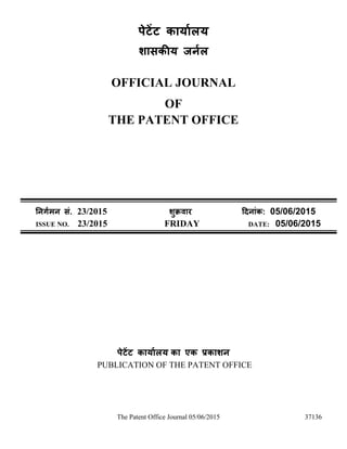
  • 1. The Patent Office Journal 05/06/2015 37136 पेट�ट कायार्ल शासक�य जनर् OFFICIAL JOURNAL OF THE PATENT OFFICE �नगर्म सं. 23/2015 शुक्रव �दनांक: 05/06/2015 ISSUE NO. 23/2015 FRIDAY DATE: 05/06/2015 पेट�ट कायार्ल का एक प्रका PUBLICATION OF THE PATENT OFFICE
  • 2. The Patent Office Journal 05/06/2015 37137 INTRODUCTION In view of the recent amendment made in the Patents Act, 1970 by the Patents (Amendment) Act, 2005 effective from 01st January 2005, the Official Journal of The Patent Office is required to be published under the Statute. This Journal is being published on weekly basis on every Friday covering the various proceedings on Patents as required according to the provision of Section 145 of the Patents Act 1970. All the enquiries on this Official Journal and other information as required by the public should be addressed to the Controller General of Patents, Designs & Trade Marks. Suggestions and comments are requested from all quarters so that the content can be enriched. ( Rajiv Aggarwal ) CONTROLLER GENERAL OF PATENTS, DESIGNS & TRADE MARKS 5TH JUNE, 2015
  • 3. The Patent Office Journal 05/06/2015 37138 CONTENTS SUBJECT PAGE NUMBER JURISDICTION : 37139 – 37140 SPECIAL NOTICE : 37141 – 37142 EARLY PUBLICATION (DELHI) : 37143 – 37168 EARLY PUBLICATION (MUMBAI) : 37169 – 37190 EARLY PUBLICATION (CHENNAI) : 37191 – 37205 EARLY PUBLICATION (KOLKATA) : 37206 – 37215 PUBLICATION AFTER 18 MONTHS (DELHI) : 37216 – 38014 PUBLICATION AFTER 18 MONTHS (MUMBAI) : 38015 – 38111 PUBLICATION AFTER 18 MONTHS (KOLKATA) : 38112 – 38126 PUBLICATION U/R 84(3) IN RESPECT OF APPLICATION FOR RESTORATION OF PATENT (MUMBAI) : 38127 PUBLICATION UNDER SECTION 43(2) IN RESPECT OF THE GRANT (DELHI) : 38128 – 38129 PUBLICATION UNDER SECTION 43(2) IN RESPECT OF THE GRANT (MUMBAI) : 38130 – 38131 PUBLICATION UNDER SECTION 43(2) IN RESPECT OF THE GRANT (CHENNAI) : 38132 – 38135 PUBLICATION UNDER SECTION 43(2) IN RESPECT OF THE GRANT (KOLKATA) : 38136 – 38139 INTRODUCTION TO DESIGN PUBLICATION : 38140 THE DESIGNS ACT 2000 SECTION 30 DESIGN ASSIGNMENT : 38141 COPYRIGHT PUBLICATION : 38142 REGISTRATION OF DESIGNS : 38143 - 38202
  • 4. The Patent Office Journal 05/06/2015 37139 THE PATENT OFFICE KOLKATA, 05/06/2015 Address of the Patent Offices/Jurisdictions The following are addresses of all the Patent Offices located at different places having their Territorial Jurisdiction on a Zonal basis as shown below:- 1 Office of the Controller General of Patents, Designs & Trade Marks, Boudhik Sampada Bhavan, Near Antop Hill Post Office,S.M.Road,Antop Hill, Mumbai – 400 037 Phone: (91)(22) 24123311, Fax : (91)(22) 24123322 E-mail: cgpdtm@nic.in 4 The Patent Office, Government of India, Intellectual Property Rights Building, G.S.T. Road, Guindy, Chennai – 600 032. Phone: (91)(44) 2250 2081-84 Fax : (91)(44) 2250 2066 E-mail: chennai-patent@nic.in  The States of Andhra Pradesh, Telangana, Karnataka, Kerala, Tamil Nadu and the Union Territories of Puducherry and Lakshadweep. 2 The Patent Office, Government of India, Boudhik Sampada Bhavan, Near Antop Hill Post Office,S.M.Road,Antop Hill, Mumbai – 400 037 Phone: (91)(22) 24137701 Fax: (91)(22) 24130387 E-mail: mumbai-patent@nic.in  The States of Gujarat, Maharashtra, Madhya Pradesh, Goa and Chhattisgarh and the Union Territories of Daman and Diu & Dadra and Nagar Haveli 5 The Patent Office (Head Office), Government of India, Boudhik Sampada Bhavan, CP-2, Sector –V, Salt Lake City, Kolkata- 700 091 Phone: (91)(33) 2367 1943/44/45/46/87 Fax: (91)(33) 2367 1988 E-Mail: kolkata-patent@nic.in  Rest of India 3 The Patent Office, Government of India, Boudhik Sampada Bhavan, Plot No. 32., Sector-14, Dwarka, New Delhi – 110075 Phone: (91)(11) 2808 1921 – 25 Fax: (91)(11) 2808 1920 & 2808 1940 E.mail: delhi-patent@nic.in  The States of Haryana, Himachal Pradesh, Jammu and Kashmir, Punjab, Rajasthan, Uttar Pradesh, Uttaranchal, Delhi and the Union Territory of Chandigarh. Website: www.ipindia.nic.in www.patentoffice.nic.in All applications, notices, statements or other documents or any fees required by the Patents Act, 1970 and The Patents (Amendment) Act, 2005 or by the Patents (Amendment) Rules, 2006 will be received only at the appropriate offices of the Patent Office. Fees: The Fees may either be paid in cash or may be sent by Bank Draft or Cheques payable to the Controller of Patents drawn on a scheduled Bank at the place where the appropriate office is situated.
  • 5. The Patent Office Journal 05/06/2015 37140 पेट�ट कायार्ल कोलकाता, �दनांक 05/06/2015 कायार्लय के �ेत्रा�धक के पते �व�भन् जगह� पर िस्थ पेट�ट कायार्ल के पते आंच�लक आधार पर द�शर् उनके प्रादे� अ�धकार �ेत के साथ नीचे �दए गए है:- 1 कायार्ल : महा�नयंत्, एकस्, अ�भकल् तथा व्यापा �चहन, एंटोप �हल डाकघर के समीप, एस. एम. रोड, एंटोप �हल, मुम्ब- 400 037, भारत, फोन: (91) (22) 24123311 फ़ै क्: (91) (22) 24123322 ई. मेल: cgpdtm@nic.in 4 पेट�ट कायार्ल, भारत सरकार इंटेलेक्चुअ प्रॉप राइट् �बिल्डं, इंडिस्ट् इस्टे एसआईडीसीओ आरएमडी गोडाउन ए�रया एडजसेन् टु ईगल फ्लास, जी. एस. ट�. रोड, गायन्ड चेन्न - 600 032. फोन: (91)(44) 2250 2081-84 फ़ै क्: (91)(44) 2250-2066 ई. मेल: chennai-patent@nic.in  आन् प्रद, तेलंगाना, कनार्ट, के रल, त�मलनाडु तथा पुडुचेर� राज् �ेत एवं संघ शा�सत �ेत, ल�द�प 2 पेट�ट कायार्ल, भारत सरकार बौ�द् संपदा भवन, एंटोप �हल डाकघर के समीप, एस. एम. रोड, एंटोप �हल, मुम्ब- 400 037, फोन: (91) (22) 24137701 फ़ै क्: (91) (22) 24130387 ई. मेल: Mumbai-patent@nic.in  गुजरात, महाराष्, मध् प्रद, गोवा तथा छत्तीसग राज् �ेत एवं संघ शा�सत �ेत, दमन तथा द�व, दादर और नगर हवेल�. 5 पेट�ट कायार्ल, भारत सरकार कोलकाता, (प्रध कायार्य) बौ�द् संपदा भवन, सीपी-2, सेक्ट- V, साल् लेक �सट�, कोलकाता-700 091, भारत. फोन: (91)(33) 2367 1943/44/45/46/87 फ़ै क्:/Fax: (91)(33) 2367 1988 ई. मेल: kolkata-patent@nic.in  भारत का अवशेष �ेत 3 पेट�ट कायार्ल, भारत सरकार बौ�द् संपदा भवन, प्लॉ सं. 32, सेक्ट- 14, द्वरका, नई �दल्ल- 110 075. फोन: (91)(11) 2808 1921-25 फ़ै क्: (91)(11) 2808 1920, 2808 1940 ई. मेल: delhi-patent@nic.in ह�रयाणा, �हमाचल प्रद, जम्म तथा कश्मी, पंजाब,राजस्था, उत्त प्रद, �दल्ल तथा उत्तरांच राज् �ेत्, एवं संघ शा�सत �ेत चंडीगढ़ वेबसाइट: http://www.ipindia.nic.in www.patentoffice.nic.in पेट�ट अ�ध�नयम, 1970 तथा पेट�ट (संशोधन) अ�ध�नयम, 2005 अथवा पेट�ट (संशोधन) �नयम, 2006 द्वार वां�छत सभी आवेदन, सूचनाए, �ववरण या अन् दस्तावे या कोई शुल् पेट�ट कायार्ल के के वल उपयुक् कायार्ल म� स्वीक ृ ह�गे। शुल्: शुल् या तो नगद रू म� या Controller of Patents के नाम म� देय ब�क ड्रा या चेक के द्वार भेजी जा सकती है जो उसी स्था के �कसी अनुसू�चत ब�क म� प्रद हो जहाँ उपयुक् कायार्ल िस्थ है ।
  • 6. The Patent Office Journal 05/06/2015 37141 SPECIAL NOTICE 18 Months publication as required under Section 11A of the Patents Act, 1970 as amended by the Patents (Amendment) Act, 2005. Notice is hereby given that any person at any time before the grant of Patent may give representation by way of opposition to the Controller of Patents at appropriate office on the ground and in a manner specified under section 25(1) of the Patents (Amendment) Act, 2005 read with Rule 55 of the Patents (Amendment) Rules, 2006. Notice is also given that if any interested person requests for copies of the complete specification, drawing and abstract of any application already published, the photocopy of the same can be supplied by the Patent Office as per the jurisdiction on payment of prescribed fees of Rs.8/- per page. If any further details are required to be obtained, the same can be provided by the respective Patent Offices on request. ( Rajiv Aggarwal ) CONTROLLER GENERAL OF PATENTS, DESIGNS & TRADE MARKS
  • 7. The Patent Office Journal 05/06/2015 37142 SPECIAL NOTICE Under the new provision of the Patents Act, 1970 as amended by the Patents (Amendment) Act, 2005 and Rules there under, Publication of the matter relating to Patents in the Official Gazette of India Part III, Section 2 has been discontinued and instead The Official Journal of the Patent Office is being published containing all the activities of The Patent Office such as publication of all the patent applications after 18th months , grant of patents & all other information in respect of the proceedings as required under the provisions of the Patents (Amendment) Act, 2005 and Rules thereunder on weekly basis on every Friday. The Journal is uploaded in the website every Friday. So Paper form and CD-ROM form of the Journal are discontinued from 01/01/2009. SPECIAL NOTICE Every effort is being taken to publish all the patent applications under section 11(A) of the Patents Act. However, if duplication of publication of any application is found, then earlier date of publication will be taken for the purpose of provisional protection for applicant and Patent Office will grant Patent not before six months from the date of second publication, provided that there is there is no third party representation.
  • 8. The Patent Office Journal 05/06/2015 37143 Early Publication: The following patent applications have been published under section 11A (2) of The Patents (Amendment) Act 2005 and rule 24A of The Patents (Amendment) Rules, 2006. Any person may file representation by way of opposition to the Controller of Patents at the appropriate office against the grant of the patent in the prescribed manner under section 25(1) of the Patents (Amendment) Act 2005 read with the rule 55 of The Patents (Amendment) Rules, 2006: (12) PATENT APPLICATION PUBLICATION (21) Application No.1085/DEL/2014 A (19) INDIA (22) Date of filing of Application :22/04/2014 (43) Publication Date : 05/06/2015 (54) Title of the invention : 90-95% METHANE PRODUCTION FROM KITCHEN WASTE BY ANAEROBIC DIGESTION PROCESS (51) International classification :C05F17/00, C05F17/02 (31) Priority Document No :NA (32) Priority Date :NA (33) Name of priority country :NA (86) International Application No Filing Date :NA :NA (87) International Publication No : NA (61) Patent of Addition to Application Number Filing Date :NA :NA (62) Divisional to Application Number Filing Date :NA :NA (71)Name of Applicant : 1)KHWAJA MOHD RAFI Address of Applicant :H.NO.339, STREET NO.12, GAFFAR MANZIL, JAMIA NAGAR, DELHI-110025. Delhi India (72)Name of Inventor : 1)KHWAJA MOHD RAFI 2)NEENA GODARA 3)MAJID JAMIL (57) Abstract : The anaerobic digestion process is usually applied for producing the Biogas out of kitchen waste. The efficiency of production of Methane gas (CH,) is 50-55% maximum for all practical models. We have developed a model where the efficiency of Methane production is gone upto 90-95%. This has become possible because the C02 which is usually 30-35% in all kind of anaerobic digestion reacts with Lime water. The reaction is shown below: Ca(OH)2(aq) + C02(g) → CaC03 (s) + H20(1) The purified Biomethane gas obtained mixed with Hydrogen gives better intensity with high calorific value. This is extremely clear gas. To get the Biomethane gas mixed with Hydrogen, an additional chamber is added, which produces the hydrogen gas. The chemical reaction to produce the hydrogen gas is as below: 2HC1+ Zn → ZnCl2 + H2 The uniqueness of mixing hydrogen gas is the work done under the research. Though the knowledge was available and hydrogen gas too but could not be exploited for such purposes. One basic reason might be due to high cost of the hydrogen gas. The process and chemical reaction proposed in the model is cheap and easy. Zinc is available at a very low cost in the market and HCI is also readily available at low cost. Both the items can be mixed out of which hydrogen gas will be produced. No. of Pages : 10 No. of Claims : 6
  • 9. The Patent Office Journal 05/06/2015 37144 (12) PATENT APPLICATION PUBLICATION (21) Application No.3669/DEL/2013 A (19) INDIA (22) Date of filing of Application :16/03/2014 (43) Publication Date : 05/06/2015 (54) Title of the invention : WATER TANK WITH CLIMATE CONTROL ARRANGEMENTS. (51) International classification :F28D15/00, F24H1/18 (31) Priority Document No :NA (32) Priority Date :NA (33) Name of priority country :NA (86) International Application No Filing Date :NA :NA (87) International Publication No : NA (61) Patent of Addition to Application Number Filing Date :NA :NA (62) Divisional to Application Number Filing Date :NA :NA (71)Name of Applicant : 1)MR. BHARAT BHUSHAN Address of Applicant :NEAR GAS AGENCY, OPPOSITE, LIONS CLUB SECTOR-2, OLD G.T. ROAD, PALWAL-121102, Haryana India (72)Name of Inventor : 1)MR. BHARAT BHUSAN (57) Abstract : Water tank with climate control arrangements allow adjusting the water temperature closer to human comfort without conventional energy. Water stored in overhead tanks made of Plastics, steel or RCC is exposed to atmospheric conditions. Prolonged sun-light & hot weather makes water hot during summers while reduced exposure to sunlight & cold weather during winters makes water cold which is opposite to Users requirement. Our system uses various arrangements to achieve the same. Reflective plates positioned over tank at prefixed locations based on the Stereographic Diagram to reduce / increase sunlight exposure. Prefixed locations are marked to assist user position the plates. Change in orientation of plates is manual or by electro-mechanical means. Further to increase conductivity on side which will face the sunlight during.winter thinner sheet/metal is used along with arrangement of fixing glass cover to create air, pocket. Regulation of opening for venting of vapour & night time convective cooling is kept. To priortise fresh supply in outlet over stored contents, fixed & floating partitions are used. System positions tanks w.r.t. Other tanks in case of multi- tank installation at same place. No. of Pages : 13 No. of Claims : 9
  • 10. The Patent Office Journal 05/06/2015 37145 (12) PATENT APPLICATION PUBLICATION (21) Application No.905/DEL/2015 A (19) INDIA (22) Date of filing of Application :31/03/2015 (43) Publication Date : 05/06/2015 (54) Title of the invention : TRANSMISSION OF STATUS INFORMATION AND PROFILE INFORMATION TO MOBILE DEVICE (51) International classification :G06F15/16 (31) Priority Document No :NA (32) Priority Date :NA (33) Name of priority country :NA (86) International Application No Filing Date :NA :NA (87) International Publication No : NA (61) Patent of Addition to Application Number Filing Date :NA :NA (62) Divisional to Application Number Filing Date :NA :NA (71)Name of Applicant : 1)Comviva Technologies Limited Address of Applicant :A-26, Info City, Sector 34, Gurgaon- 122001, Haryana, India (72)Name of Inventor : 1)JAIN, Manish Kumar 2)GOYAL, Gaurav (57) Abstract : The invention relates to transmission of status information and profile information to mobile device. In one embodiment, a method (100, 200) for transmission of status and profile information comprises: receiving (101, 201) a request for status information set by user of a called mobile device and profile information set by a user of a calling mobile device from a mobile switching centre (MSC); retrieving a status information, profile information and either of a call allowance information or an authorised contact list associated with the status information, the status information indicating a time period of validity of the status information; generating (103) a push message including either the retrieved status information or a modified status information as locally derived based on the time period; and transmitting (104, 204) the push message to a push message gateway communicatively coupled to the calling mobile device and to the called mobile device. No. of Pages : 70 No. of Claims : 36
  • 11. The Patent Office Journal 05/06/2015 37146 (12) PATENT APPLICATION PUBLICATION (21) Application No.1246/DEL/2015 A (19) INDIA (22) Date of filing of Application :06/05/2015 (43) Publication Date : 05/06/2015 (54) Title of the invention : AN AUTOMATED NAVIGATION SYSTEM AND METHOD FOR ITEM RETRIEVAL AND DEPOSITION (51) International classification :B66C19/00 (31) Priority Document No :NA (32) Priority Date :NA (33) Name of priority country :NA (86) International Application No Filing Date :NA :NA (87) International Publication No : NA (61) Patent of Addition to Application Number Filing Date :NA :NA (62) Divisional to Application Number Filing Date :NA :NA (71)Name of Applicant : 1)The Hi-Tech Robotic Systemz Ltd. Address of Applicant :A-18, Sector -33/34, Infocity I, Gurgaon - 122001, Haryana, India (72)Name of Inventor : 1)Anuj Kapuria 2)Shailesh Sule 3)Jayant Bansal (57) Abstract : According to the preferred embodiment of the present invention, an automated navigation system and method for item retrieval and deposition. The system comprises a plurality of robotic vehicles deployed in a closed environment to transport items from one depository location to another depository location; a central server to control the navigation of said robotic vehicles through a wireless communication; wherein said robotic vehicle comprises a first set of drive wheels to dynamically navigate on floor and a second set of drive wheels to navigate in depositories with mechanically guided paths. No. of Pages : 25 No. of Claims : 36
  • 12. The Patent Office Journal 05/06/2015 37147 (12) PATENT APPLICATION PUBLICATION (21) Application No.2429/DELNP/2015 A (19) INDIA (22) Date of filing of Application :25/03/2015 (43) Publication Date : 05/06/2015 (54) Title of the invention : DRIVE MEMBER SELECTION (51) International classification :F16H63/18,F16H63/30,F16D41/18 (31) Priority Document No :1217100.5 (32) Priority Date :25/09/2012 (33) Name of priority country :U.K. (86) International Application No Filing Date :PCT/GB2013/000406 :25/09/2013 (87) International Publication No :WO 2014/049317 (61) Patent of Addition to Application Number Filing Date :NA :NA (62) Divisional to Application Number Filing Date :NA :NA (71)Name of Applicant : 1)QINETIQ LIMITED Address of Applicant :Cody Technology Park Ively Road Farnborough Hampshire GU14 0LX U.K. (72)Name of Inventor : 1)THOMPSON Robert William (57) Abstract : A drive member selection mechanism is described comprising at least one drive member and at least two selector members wherein the drive member comprises a first and second face and further comprises on each face at least one projection and the selector members comprise on at least one face thereof at least one complementary projection arranged to selectively engage with a projection of a drive member the arrangement being such that the projection(s) of a selector member and the projection(s) of the first face of a drive member may be drivingly engaged in a first torque connection and the projection(s) of a selector member and the projection(s) of the second face of a drive member may be drivingly engaged in a second torque connection wherein the second torque connection is opposed to the first torque connection. No. of Pages : 37 No. of Claims : 27
  • 13. The Patent Office Journal 05/06/2015 37148 (12) PATENT APPLICATION PUBLICATION (21) Application No.889/DEL/2015 A (19) INDIA (22) Date of filing of Application :30/03/2015 (43) Publication Date : 05/06/2015 (54) Title of the invention : SYSTEM AND METHOD FOR CONFIGURING A RING BACK TONE (51) International classification :H04W4/16, H04W88/18 (31) Priority Document No :NA (32) Priority Date :NA (33) Name of priority country :NA (86) International Application No Filing Date :NA :NA (87) International Publication No : NA (61) Patent of Addition to Application Number Filing Date :NA :NA (62) Divisional to Application Number Filing Date :NA :NA (71)Name of Applicant : 1)Comviva Technologies Limited Address of Applicant :A-26, Info City, Sector 34, Gurgaon- 122001, Haryana, India (72)Name of Inventor : 1)BHARGAVA, Mukesh 2)JAIN, Manish Kumar (57) Abstract : The present invention relates to a system and methods for providing Ring Back Tones corresponding to a selected relationship. The method comprises: analysing call history of a subscriber to derive a set of frequently contacted numbers, presenting to the subscriber or the first participant atleast one possible relationship between the subscriber and the first participant, presenting to the subscriber or the first participant a plurality of Ring Back Tones corresponding to the selected relationship and provisioning the selected RBT for calls involving the subscriber and the first participant. No. of Pages : 31 No. of Claims : 24
  • 14. The Patent Office Journal 05/06/2015 37149 (12) PATENT APPLICATION PUBLICATION (21) Application No.970/DEL/2015 A (19) INDIA (22) Date of filing of Application :06/04/2015 (43) Publication Date : 05/06/2015 (54) Title of the invention : SYSTEM AND METHOD FOR KEYWORD BASED TESTING OF CUSTOM COMPONENTS (51) International classification :H04L12/24, H04L29/08, (31) Priority Document No :NA (32) Priority Date :NA (33) Name of priority country :NA (86) International Application No Filing Date :NA :NA (87) International Publication No : NA (61) Patent of Addition to Application Number Filing Date :NA :NA (62) Divisional to Application Number Filing Date :NA :NA (71)Name of Applicant : 1)HCL Technologies Limited Address of Applicant :B-39, Sector 1, Noida - 201 301, Uttar Pradesh, India (72)Name of Inventor : 1)SINGH, Daljeet 2)DEY, Sourav (57) Abstract : The present disclosure relates to system(s) and method(s) for testing a custom component associated with a software application. Initially a set of custom components and a set of metadata associated with the set of components are received from a third party developer in an XML file. The metadata comprises a plurality of attributes categorized into a plurality of categories. Further, the set of custom components and the set of metadata are stored in an object repository. In the next step, a custom component from the software application is selected for testing over a test grid. Further, metadata associated with the custom component is identified from the object repository. Further, an attribute of each category from the metadata corresponding to the custom component is selected in order to generate an event set corresponding to the custom component wherein the event set comprises the attribute selected for testing the custom component. No. of Pages : 24 No. of Claims : 15
  • 15. The Patent Office Journal 05/06/2015 37150 (12) PATENT APPLICATION PUBLICATION (21) Application No.1188/DEL/2015 A (19) INDIA (22) Date of filing of Application :29/04/2015 (43) Publication Date : 05/06/2015 (54) Title of the invention : TEST SUITE MINIMIZATION (51) International classification :G06F11/36 (31) Priority Document No :NA (32) Priority Date :NA (33) Name of priority country :NA (86) International Application No Filing Date :NA :NA (87) International Publication No : NA (61) Patent of Addition to Application Number Filing Date :NA :NA (62) Divisional to Application Number Filing Date :NA :NA (71)Name of Applicant : 1)HCL Technologies Ltd Address of Applicant :B-39, Sector 1, Noida 201 301, Uttar Pradesh, India (72)Name of Inventor : 1)CHACKO, Simy 2)KANAKADANDI, Satya Sai Prakash 3)DHANYAMRAJU, S U M Prasad (57) Abstract : Disclosed is a method and system for classifying test cases. In one implementation, the method comprises creating a test step master list comprising a plurality of test case, one more test step associated with the plurality of test case, and a test step identification number associated with the one more test step. Further, the method comprises generating a sequence diagram for each of the plurality of test cases based on the test step master list. Furthermore, the method comprises classifying, by the processor, each of the plurality of test cases in to an independent test case or an asynchronous test case or a synchronous test case based on the sequence diagram. No. of Pages : 23 No. of Claims : 27
  • 16. The Patent Office Journal 05/06/2015 37151 (12) PATENT APPLICATION PUBLICATION (21) Application No.820/DEL/2015 A (19) INDIA (22) Date of filing of Application :24/03/2015 (43) Publication Date : 05/06/2015 (54) Title of the invention : CAR JACK WITH DETACHABLE OR INTEGRATED UNIVERSAL JOINT MECHANISM (51) International classification :B66F5/04 (31) Priority Document No :NA (32) Priority Date :NA (33) Name of priority country :NA (86) International Application No Filing Date :NA :NA (87) International Publication No : NA (61) Patent of Addition to Application Number Filing Date :NA :NA (62) Divisional to Application Number Filing Date :NA :NA (71)Name of Applicant : 1)AMRIT LAL Address of Applicant :Flat No. 401, Tower E1, Gurgaon 21. Vatika India Next Sector 83, Gurgaon, Haryana 122004, India (72)Name of Inventor : 1)AMRIT LAL (57) Abstract : This invention relates to automotive jacks used for lifting vehicles and more particularly to a light weight, compact jack which is inexpensive to manufacture, easy to operate. The present disclosure relates to a universal joint mechanism applied to a car jack that makes its operation very easy and user friendly. No. of Pages : 15 No. of Claims : 4
  • 17. The Patent Office Journal 05/06/2015 37152 (12) PATENT APPLICATION PUBLICATION (21) Application No.915/DEL/2015 A (19) INDIA (22) Date of filing of Application :31/03/2015 (43) Publication Date : 05/06/2015 (54) Title of the invention : PREFERENTIAL ROUTING IN PARALLEL TRANSACTION BASED MOBILE POINT-OF-SALE SYSTEM (51) International classification :G06Q20/10 (31) Priority Document No :NA (32) Priority Date :NA (33) Name of priority country :NA (86) International Application No Filing Date :NA :NA (87) International Publication No : NA (61) Patent of Addition to Application Number Filing Date :NA :NA (62) Divisional to Application Number Filing Date :NA :NA (71)Name of Applicant : 1)Comviva Technologies Limited Address of Applicant :A-26, Info City, Sector 34, Gurgaon- 122001, Haryana, India (72)Name of Inventor : 1)BHALLA, Gurpreet Singh 2)MYLAPALLI, Deepak V S 3)KOMPALLY, Santosh (57) Abstract : The invention provides method and system for implementing preferential routing in a mobile point of sale system. The method includes establishing a session by a host device with a plurality of card reader units. The host device simultaneously establishes a plurality of sessions, wherein the host device receives from each of the plurality of card reader units a processing request through corresponding session. The processing request comprises a first identifier data and a second identifier data. The host device assigns a priority value to each of the processing request based on the second identifier and transmits each of the processing request based on the priority value thus assigned. No. of Pages : 24 No. of Claims : 11
  • 18. The Patent Office Journal 05/06/2015 37153 (12) PATENT APPLICATION PUBLICATION (21) Application No.1104/DEL/2015 A (19) INDIA (22) Date of filing of Application :21/04/2015 (43) Publication Date : 05/06/2015 (54) Title of the invention : AUTOMATIC PARKING SYSTEM (51) International classification :E04H6/18 (31) Priority Document No :NA (32) Priority Date :NA (33) Name of priority country :NA (86) International Application No Filing Date :NA :NA (87) International Publication No : NA (61) Patent of Addition to Application Number Filing Date :NA :NA (62) Divisional to Application Number Filing Date :NA :NA (71)Name of Applicant : 1)RAJ SATYAM Address of Applicant :M-98 CANNAUGHT PLACE WESTERN INDIA BUILDING, OPP HALDIRAM, NEW DELHI India (72)Name of Inventor : 1)RAJ SATYAM (57) Abstract : This invention deals how the car will be Automatically parked in an empty space and will come back by itself whenever the owner wants it to. It consist a trolley with Resistance box and different structures helpful in different location. It also consist of direction deflection of trolley without sensors according to the requirement of that place ie. Automatic track changing of trolley. Automatic start of trolly from rest whenever switch will be pressed in control room. Anti collision technique due to positioned switch. Automatic shift of curved metal according to requirement. It also consists of position specifying technique with the help of resistance box. The can location will be displayed in control room by digital ammeter. No. of Pages : 24 No. of Claims : 8
  • 19. The Patent Office Journal 05/06/2015 37154 (12) PATENT APPLICATION PUBLICATION (21) Application No.1075/DEL/2015 A (19) INDIA (22) Date of filing of Application :17/04/2015 (43) Publication Date : 05/06/2015 (54) Title of the invention : DIFFRACTIVE-REFRACTIVE LENS (51) International classification :A61F2/1618 (31) Priority Document No :NA (32) Priority Date :NA (33) Name of priority country :NA (86) International Application No Filing Date :NA :NA (87) International Publication No : NA (61) Patent of Addition to Application Number Filing Date :NA :NA (62) Divisional to Application Number Filing Date :NA :NA (71)Name of Applicant : 1)ROOP Prakhyat Address of Applicant :c/o Dr.Roop, 348, Govind Lok, E.K. Road, Meerut- 250001, Uttar Pradesh, India (72)Name of Inventor : 1)ROOP Prakhyat (57) Abstract : An intraocular lens (100) is provided. The intraocular lens (100) includes an anterior surface (102) and a posterior surface (104). The posterior surface (104) defines a plurality of circular bands (114). Each circular band (114) is offset from its adjacent circular band (114) along a longitudinal axis (106) of the intraocular lens (100), wherein a surface (120) extends along the longitudinal axis (106) between peripheries of adjacent circular bands (114). Reference figure: FIG. 1C No. of Pages : 15 No. of Claims : 8
  • 20. The Patent Office Journal 05/06/2015 37155 (12) PATENT APPLICATION PUBLICATION (21) Application No.1238/DEL/2014 A (19) INDIA (22) Date of filing of Application :08/05/2014 (43) Publication Date : 05/06/2015 (54) Title of the invention : METHOD OF MAKING CO-EXTRUDED TAPE AND FABRIC AND BAG MADE THEREOF` (51) International classification :C09J7/02, C09J153/00, (31) Priority Document No :NA (32) Priority Date :NA (33) Name of priority country :NA (86) International Application No Filing Date :NA :NA (87) International Publication No : NA (61) Patent of Addition to Application Number Filing Date :NA :NA (62) Divisional to Application Number Filing Date :NA :NA (71)Name of Applicant : 1)CHATURVEDI, ASHOK Address of Applicant :305, III FLOOR, BHANOT CORNER, PAMPOSH ENCLAVE, GK-1, NEW DELHI-110048 India (72)Name of Inventor : 1)CHATURVEDI, ASHOK (57) Abstract : A co-extruded multi-layered tape for woven substrates and woven bags is provided. he multi-layered tape includes a middle polymeric layer coextruded with at least one external layer configured on each side of the middle polymeric layer. The external layers are coextruded with a low temperature sealable material, such that the external layers on each side of the middle polymeric layer have same sealing properties. No. of Pages : 17 No. of Claims : 13
  • 21. The Patent Office Journal 05/06/2015 37156 (12) PATENT APPLICATION PUBLICATION (21) Application No.2628/DELNP/2015 A (19) INDIA (22) Date of filing of Application :31/03/2015 (43) Publication Date : 05/06/2015 (54) Title of the invention : ELECTRODE BOILER WITH ELECTRODES UNIT (51) International classification :F22B1/30,H05B3/03,H05B3/60 (31) Priority Document No :NA (32) Priority Date :NA (33) Name of priority country :NA (86) International Application No Filing Date :PCT/IB2012/003083 :05/12/2012 (87) International Publication No :WO 2014/087190 (61) Patent of Addition to Application Number Filing Date :NA :NA (62) Divisional to Application Number Filing Date :NA :NA (71)Name of Applicant : 1)KIM No Eul Address of Applicant :Bansong 2-Dong 216-50 Haeundae gu Busan Republic of Korea (72)Name of Inventor : 1)ILIN, Andrey, Pavlovich (57) Abstract : The invention relates to heat engineering power engineering and the field of electric heating of liquids water for instance; it can be used in circulation water heating systems and hot water supply and as a universal device for diverse electric heaters. An object of the invention are to enhance the ease of fabrication fabricability and operability for block electrodes and electrode heating boilers on the whole to increase the reliability of device both in static and dynamic modes ones. The invention meets an object of extended performance capabilities versatility and flexibility of the device potential diversification and enhancement of adaptability in solving particular problems. Moreover the invention allows improvement of convection in water heating boilers and reduction of uniformity of sludge and rust deposition on electrodes thus increasing the heater effective performance time. The invention object comprises an improvement of protection against breakdowns between the electrodes as well phase current load imbalance reduction electrode protection against non uniform deformation during operation in dynamic conditions. It is also an object of the invention to extend i the range of constructional capacity control without design and dimensional changes. Fig.2 provides a schematic of electrodes (1) arrangement on the basis (3) located on the inner case (2) side with electrodes (1) slightly deviating from the longitudinal symmetric axis of the case (2) and irregularly spaced on the basis electrode longitudinal axes deviating from each other at small angles. (4) outer electrode terminals (1). No. of Pages : 35 No. of Claims : 28
  • 22. The Patent Office Journal 05/06/2015 37157 (12) PATENT APPLICATION PUBLICATION (21) Application No.2629/DELNP/2015 A (19) INDIA (22) Date of filing of Application :31/03/2015 (43) Publication Date : 05/06/2015 (54) Title of the invention : POWER THYRISTOR UNIT COOLING SYSTEM (51) International classification :H01L23/473,H05K7/20 (31) Priority Document No :NA (32) Priority Date :NA (33) Name of priority country :NA (86) International Application No Filing Date :PCT/IB2013/001292 :24/04/2013 (87) International Publication No :WO 2014/174336 (61) Patent of Addition to Application Number Filing Date :NA :NA (62) Divisional to Application Number Filing Date :NA :NA (71)Name of Applicant : 1)KIM No Eul Address of Applicant :216 50 Bansong 2 Dong Haeundae gu Busan Republic of Korea (72)Name of Inventor : 1)ILIN, Andrey, Pavlovich (57) Abstract : The invention relates to heat technology equipment and semiconductor devices for electric control and adjustment power engineering and the heating by using electricity for the heating of a liquid for example water steam generation direct transformation of electric power into heat. Naturally the invention is meant for liquid cooling of power electric semiconductor devices of control and adjustment in particular for the cooling of semiconducting thyristors. Another task is to simplify the requirements to the assembling accuracy of the entire unit and the cooling system by following the recommended type of the housing design as well as the type of thyristors arrangement against each other and the device housing. The invention enables convection conditions for circulating liquid for the recommended thyristors arrangement. Fig. 17 is a diagram of the embodiment 2 wherein the power thyristors or triacs (1) are set non symmetrically and non uniformly on the body (2) or on an interim plate (3). The body cavity (6) of the device in general case could have such a shape that the contours of longitudinal (4) and lateral (7) sections would make random smooth closed curves. There at the outer contour in its longitudinal (5) and lateral (8) sections could be a shape of a random closed contour. No. of Pages : 33 No. of Claims : 13
  • 23. The Patent Office Journal 05/06/2015 37158 (12) PATENT APPLICATION PUBLICATION (21) Application No.1249/DEL/2015 A (19) INDIA (22) Date of filing of Application :06/05/2015 (43) Publication Date : 05/06/2015 (54) Title of the invention : SYSTEM AND METHOD FOR PROVIDING CODE COVERAGE (51) International classification :G06F9/44 (31) Priority Document No :NA (32) Priority Date :NA (33) Name of priority country :NA (86) International Application No Filing Date :NA :NA (87) International Publication No : NA (61) Patent of Addition to Application Number Filing Date :NA :NA (62) Divisional to Application Number Filing Date :NA :NA (71)Name of Applicant : 1)HCL Technologies Ltd Address of Applicant :B-39, Sector 1, Noida 201 301, Uttar Pradesh, India (72)Name of Inventor : 1)YADAVA, Sanjay Kumar 2)SELWYN, Johnson 3)DHANYAMRAJU, S U M Prasad 4)JAIN, Ambica 5)SIVANESAN, Arivukarasu (57) Abstract : Disclosed is a method and system for providing code coverage of a code. The system may determine a type of file comprising the code. The system may extract a source code from the code, based on the type of file. The system may process the source code for generating a structured source code. The system may determine code coverage of the structured source code by executing test cases upon the structured source code. The system may provide a code coverage report comprising line coverages, program coverages, and code block coverages of the structured source code. No. of Pages : 23 No. of Claims : 23
  • 24. The Patent Office Journal 05/06/2015 37159 (12) PATENT APPLICATION PUBLICATION (21) Application No.920/DEL/2015 A (19) INDIA (22) Date of filing of Application :31/03/2015 (43) Publication Date : 05/06/2015 (54) Title of the invention : METHOD AND DEVICE FOR PROVISIONING OF PLURALITY OF SERVICES (51) International classification :H04M3/00, H04M1/00 (31) Priority Document No :NA (32) Priority Date :NA (33) Name of priority country :NA (86) International Application No Filing Date :NA :NA (87) International Publication No : NA (61) Patent of Addition to Application Number Filing Date :NA :NA (62) Divisional to Application Number Filing Date :NA :NA (71)Name of Applicant : 1)Comviva Technologies Limited Address of Applicant :A-26, Info City, Sector 34, Gurgaon- 122001, Haryana, India (72)Name of Inventor : 1)NAIR, Rakesh Sasidharan (57) Abstract : The present idea discloses a method for simultaneously provisioning multiple services as offered by a service provider thereby improving provisioning experience for the customers. On receiving a message comprising offer for multiple services, the customer may send a request comprising details of a plurality of services that (e.g., service 1, service 3 and service 5). Subsequently, a proxy account number on the basis of contents of the request is generated, the proxy account number is mapped to an actual account number of the customer and the proxy account number is transmitted to the customer. Thereafter, a message is received against the proxy account number and at least one configuring message for configuring a plurality of services is generated and transmitted. No. of Pages : 25 No. of Claims : 12
  • 25. The Patent Office Journal 05/06/2015 37160 (12) PATENT APPLICATION PUBLICATION (21) Application No.888/DEL/2015 A (19) INDIA (22) Date of filing of Application :30/03/2015 (43) Publication Date : 05/06/2015 (54) Title of the invention : METHOD OF MANAGING USER SUBSCRIPTION ACCOUNTS AND SYSTEM THEREOF (51) International classification :G06F21/24, H04L29/08 (31) Priority Document No :NA (32) Priority Date :NA (33) Name of priority country :NA (86) International Application No Filing Date :NA :NA (87) International Publication No : NA (61) Patent of Addition to Application Number Filing Date :NA :NA (62) Divisional to Application Number Filing Date :NA :NA (71)Name of Applicant : 1)Comviva Technologies Limited Address of Applicant :A-26, Info City, Sector 34, Gurgaon- 122001, Haryana, India (72)Name of Inventor : 1)AHMED, Sabir 2)NAIR, Rakesh Sasidharan (57) Abstract : The invention provides method and system for managing user subscription accounts. The method includes the steps of receiving a request for linking comprising a primary identifier and at least one secondary identifier, the primary identifier being associated with a primary subscription account and each of said at least one secondary identifier being associated with a corresponding secondary subscription account. The method involves linking at least one of said secondary subscription account with said primary subscription account and receiving a primary authentication request directed towards the primary subscription account, the primary authentication request being for a first value. The method further includes automatically generating a secondary authentication request directed towards the primary subscription account and at least one tertiary authentication request directed towards said at least one or more secondary subscription account linked with said primary subscription account, each of the secondary authentication request and the at least one tertiary authentication request containing respective values whose sum is equal to the first value. No. of Pages : 26 No. of Claims : 17
  • 26. The Patent Office Journal 05/06/2015 37161 (12) PATENT APPLICATION PUBLICATION (21) Application No.4023/DEL/2014 A (19) INDIA (22) Date of filing of Application :30/12/2014 (43) Publication Date : 05/06/2015 (54) Title of the invention : METHOD AND DEVICE FOR PROVIDING SPONSORED COMMUNICATION SERVICES TO LOAN NON-ELIGIBLE SUBSCRIBERS (51) International classification :H04W8/20, H04M1/00 (31) Priority Document No :NA (32) Priority Date :NA (33) Name of priority country :NA (86) International Application No Filing Date :NA :NA (87) International Publication No : NA (61) Patent of Addition to Application Number Filing Date :NA :NA (62) Divisional to Application Number Filing Date :NA :NA (71)Name of Applicant : 1)Comviva Technologies Limited Address of Applicant :A-26, Info City, Sector 34, Gurgaon- 122001, Haryana, India (72)Name of Inventor : 1)JAIN, Manish Kumar 2)RABRA, Arun (57) Abstract : The present invention provides a method for providing sponsored communication services in a telecommunication network to loan non-eligible subscribers comprising: receiving, by a proxy device, a communication request originating from an initiating party and forwarding the communication request to a loan granting system; receiving, by the proxy device, a signal indicative of loan refusal (because the subscriber is a loan non-eligible subscriber) from the loan granting system; informing the initiating party, by the proxy device, terms of sponsorship and seeking approval from the initiating party; receiving, by the proxy device, a signal indicative of approval by the initiating party; and sending, by the proxy device, routing information to a routing device for storing in respect of the initiating party, the routing device acting upon the routing information while providing a communication service. No. of Pages : 23 No. of Claims : 14
  • 27. The Patent Office Journal 05/06/2015 37162 (12) PATENT APPLICATION PUBLICATION (21) Application No.1248/DEL/2015 A (19) INDIA (22) Date of filing of Application :06/05/2015 (43) Publication Date : 05/06/2015 (54) Title of the invention : TESTING SCREENS OF A MULTI-SCREEN DEVICE (51) International classification :G06F3/14, G09G5/00 (31) Priority Document No :NA (32) Priority Date :NA (33) Name of priority country :NA (86) International Application No Filing Date :NA :NA (87) International Publication No : NA (61) Patent of Addition to Application Number Filing Date :NA :NA (62) Divisional to Application Number Filing Date :NA :NA (71)Name of Applicant : 1)HCL Technologies Ltd Address of Applicant :B-39, Sector 1, Noida 201301, Uttar Pradesh, India (72)Name of Inventor : 1)SURAPARAJU, Rajesh Babu 2)SUBBARAYAN, Arun Prasad (57) Abstract : Disclosed is a method for testing screens of a multi-screen device. The multi-screen devicemay establish connections between a plurality of users and a plurality of screens, based on access requests. The multi-screen devicemay receive commands to be executed on corresponding screens. The multi-screen devicemay capture responses of the executionby using a frame grab technique. The multi- screen devicemay determine a performance of each screen of the plurality of screens based on the captured responses. The multi- screen devicemay thus test the plurality of screens based on the performance. No. of Pages : 17 No. of Claims : 9
  • 28. The Patent Office Journal 05/06/2015 37163 (12) PATENT APPLICATION PUBLICATION (21) Application No.500/DEL/2015 A (19) INDIA (22) Date of filing of Application :23/02/2015 (43) Publication Date : 05/06/2015 (54) Title of the invention : PRISMAWIPE-PRISMATIC WIPER ASSEMBLY FOR EDGE-TO-EDGE WINDSHEILD CLEANING. (51) International classification :B60S1/38 (31) Priority Document No :NA (32) Priority Date :NA (33) Name of priority country :NA (86) International Application No Filing Date :NA :NA (87) International Publication No : NA (61) Patent of Addition to Application Number Filing Date :NA :NA (62) Divisional to Application Number Filing Date :NA :NA (71)Name of Applicant : 1)ER. FARAZ AHMAD Address of Applicant :I-21, EKTA NAGAR CAMPUS, ALIGARH (UP)-202001 Uttar Pradesh India 2)DR. AMEER AZAM (72)Name of Inventor : 1)ER. FARAZ AHMAD 2)DR. AMEER AZAM (57) Abstract : This invention relates to a wiper system for motor vehicles or the like and is named as PrismaWipe- Prismatic Wiper Assembly for Edge to Edge Cleaning. The described invention is a two link prismatic mechanism that actuates in a profile such that it wipes the complete rectangular area of the windshield: It uses an actuator fed by a controller that actuates it in the given profile. The design of this invention is better than the conventional wiper assembly that uses a fixed length wiper blade for sweeping a semi-circular region on the windshield. The described invention is capable to run in prismatic as well as conventional mode. No. of Pages : 10 No. of Claims : 5
  • 29. The Patent Office Journal 05/06/2015 37164 (12) PATENT APPLICATION PUBLICATION (21) Application No.1015/DEL/2015 A (19) INDIA (22) Date of filing of Application :12/04/2015 (43) Publication Date : 05/06/2015 (54) Title of the invention : AN ADD ON DEVICE TO SMART RATION CARD (51) International classification :G06Q10/00 (31) Priority Document No :NA (32) Priority Date :NA (33) Name of priority country :NA (86) International Application No Filing Date :NA :NA (87) International Publication No : NA (61) Patent of Addition to Application Number Filing Date :NA :NA (62) Divisional to Application Number Filing Date :NA :NA (71)Name of Applicant : 1)Manoj Kumar Address of Applicant :S/o Jagdish Chander, Jawhar Jyoti Jyotipram, Damuadunga, Haldwani, Nainital (Uttrakhand), Pin Code: 263139 Uttarakhand India (72)Name of Inventor : 1)Manoj Kumar (57) Abstract : Present invention relates to a ration card system and a device operating thereto, which comprises: a RFID card/tag; a hand held device, comprising a RF module, display unit, a switch array, a microcontroller board and a battery; a server comprising of a RF module, a microcontroller board, personal computer, and a GSM modem; wherein the RFID card/tag has a unique identification number for authentication. No. of Pages : 9 No. of Claims : 6
  • 30. The Patent Office Journal 05/06/2015 37165 (12) PATENT APPLICATION PUBLICATION (21) Application No.202/DEL/2013 A (19) INDIA (22) Date of filing of Application :28/01/2013 (43) Publication Date : 05/06/2015 (54) Title of the invention : PROCESS FOR PRODUCING TIO2 BASED PHOTOCATALYTIC COATING, THE TIO2 BASED COATING OBTAINED BY THE PROCESS AND VARIOUS ARTICLES WITH COATING APPLIED THEREON (51) International classification :C08L89/00, C08K5/00 (31) Priority Document No :NA (32) Priority Date :NA (33) Name of priority country :NA (86) International Application No Filing Date :NA :NA (87) International Publication No : NA (61) Patent of Addition to Application Number Filing Date :NA :NA (62) Divisional to Application Number Filing Date :NA :NA (71)Name of Applicant : 1)ROSARIO COSMETICS PVT. LTD. Address of Applicant :UNIVERSAL TRADE TOWER, SECTOR 49, SOHNA ROAD, GURGAON-122001 HARYANA India (72)Name of Inventor : 1)GUNAWARDANA, MANJU (57) Abstract : The present invention discloses a water soluble photocatalytic material capable of being adhered to an article by a conventional coating process.The photocatalytic material includes a doped metal oxide substrate capable of exhibiting photocatalytic behavior on being 10 exposed to visible light, wherein particle size of doped metal oxide substrate ranges from about 18 nanometer (nm) to about 35 nm. Further, the photocatalytic material includes a polymeric adhesive for improving the adhering property of the doped metal oxide substrate on the article. The present invention also relates to a process for producing the water soluble photocatalytic material. It further relates to an air purifying article on which the said 15 photocatalytic material is applied to. No. of Pages : 20 No. of Claims : 18
  • 31. The Patent Office Journal 05/06/2015 37166 (12) PATENT APPLICATION PUBLICATION (21) Application No.230/DEL/2014 A (19) INDIA (22) Date of filing of Application :27/01/2014 (43) Publication Date : 05/06/2015 (54) Title of the invention : UNIVERSAL ADVANCE TIME SYSTEM (51) International classification :F16D3/00 (31) Priority Document No :NA (32) Priority Date :NA (33) Name of priority country :NA (86) International Application No Filing Date :NA :NA (87) International Publication No : NA (61) Patent of Addition to Application Number Filing Date :NA :NA (62) Divisional to Application Number Filing Date :NA :NA (71)Name of Applicant : 1)SANJAY KUMAR PANERI Address of Applicant :215-GANESH COLONY, RAOJI-KA- HATA, UDAIPUR (RAJ.)-INDIA-313001. (72)Name of Inventor : 1)SANJAY KUMAR PANERI (57) Abstract : Universal advance time systems has 1000 degree of longitude instead of 360 degree and there is no east and west division in longitude. At present each degree has distance of 111.319 kilometer to other degree and each degree have travel on equator in 4 minutes but our propose time system have 1000 degree travel in 1000 minutes means one degree one minutes each degree has 40.075 kilometer distance to other degree so this proposed time system have more accurate and easy system to find out the any location on the earth. For e.g. point of 115.315 longitude has 1 hour 15 minutes 31.5 seconds it means we can get most accurate and most simple time of the any location. Universal advance time systems has increase degree 360 to 1000 so increase of degree near about 3 times therefore every country find its ,more accurate time than present. It is more accurate to find any small location without any confusion east and west division because it has 0 to 1000 degree longitude only. No. of Pages : 21 No. of Claims : 6
  • 32. The Patent Office Journal 05/06/2015 37167 (12) PATENT APPLICATION PUBLICATION (21) Application No.2908/DEL/2014 A (19) INDIA (22) Date of filing of Application :12/10/2014 (43) Publication Date : 05/06/2015 (54) Title of the invention : AN AUTOMATED IRRIGATION SYSTEM (51) International classification :A01G25/00, G05D11/00, (31) Priority Document No :NA (32) Priority Date :NA (33) Name of priority country :NA (86) International Application No Filing Date :NA :NA (87) International Publication No : NA (61) Patent of Addition to Application Number Filing Date :NA :NA (62) Divisional to Application Number Filing Date :NA :NA (71)Name of Applicant : 1)Pradeep Kumar Address of Applicant :S/o Krishan Kumar V.P.O.- Bahia, Tehsil-Rania, District-Sirsa, Haryana (125075) India 2)Prof. (Dr.) Pankaj Chandna (72)Name of Inventor : 1)Pradeep Kumar 2)Prof. (Dr.) Pankaj Chandna (57) Abstract : Present invention relates to an automated irrigation system. More particularly, present invention relates to an irrigation system wherein the irrigation system adjusts the flow and amount of water in field. No. of Pages : 24 No. of Claims : 5
  • 33. The Patent Office Journal 05/06/2015 37168 (12) PATENT APPLICATION PUBLICATION (21) Application No.465/DEL/2015 A (19) INDIA (22) Date of filing of Application :18/02/2015 (43) Publication Date : 05/06/2015 (54) Title of the invention : RENEWABLE ENERGY DRIVEN ENVIRONMENT FRIENDLY ENERGY EFFICIENT ECONOMICAL ELECTRICAL VEHICLE (51) International classification :B63H21/00, H02J7/14, (31) Priority Document No :NA (32) Priority Date :NA (33) Name of priority country :NA (86) International Application No Filing Date :NA :NA (87) International Publication No : NA (61) Patent of Addition to Application Number Filing Date :NA :NA (62) Divisional to Application Number Filing Date :NA :NA (71)Name of Applicant : 1)SINGH HEMANT Address of Applicant :2 BHAWANI SINGH LANE, B.S. ROAD, JAIPUR-1, RAJASTHAN, INDIA. (72)Name of Inventor : 1)SINGH HEMANT (57) Abstract : The invention is related to the field of Automobile Engineering. A Nonpolluting, Energy Efficient and Economical Vehicle are the need of the hour. The invention is an introduction of Vehicle which is a Complete System of Environment Friendly Vehicle. It is nonpolluting because it runs on Solar and Wind Energy driven by Electric Motor. It is very energy efficient because .it Generates and Saves .Energy during operation. To Generate Energy during operation it utilizes Air Resistance by adopting Air Generator and vehicles Momentum by adopting Regenerative System. It also saves Energy during operation by utilizing Rolling Momentum of the vehicle through Single .Directional Clutch in combination with Electronic Gates. It is economical because its operating cost on fuel is zero, maintenance cost is low and initial cost is also low. All this makes this unique invention. It is a vehicle of future with Clean Technology and compatible with present transportation. No. of Pages : 29 No. of Claims : 5
  • 34. The Patent Office Journal 05/06/2015 37169 (12) PATENT APPLICATION PUBLICATION (21) Application No.2035/MUM/2015 A (19) INDIA (22) Date of filing of Application :26/05/2015 (43) Publication Date : 05/06/2015 (54) Title of the invention : MIST NOZZLE AND METHOD OF MAKING THE SAME (51) International classification :B05B1/34, B05B17/00 (31) Priority Document No :NA (32) Priority Date :NA (33) Name of priority country :NA (86) International Application No Filing Date :NA :NA (87) International Publication No : NA (61) Patent of Addition to Application Number Filing Date :NA :NA (62) Divisional to Application Number Filing Date :NA :NA (71)Name of Applicant : 1)SAPALI SHIVALINGAPPA NAGAPPA Address of Applicant :FLAT NO.06, ANANDI BAUG APARTMENT, TEJASNAGAR, BEHIND MANTRI PARK, KOTHRUD, PUNE, MAHARASHTRA - 38. India 2)AHUJA BHARATKUMAR BHAGATRAJ 3)AVINASH M. DESHMUKH 4)KALE SANDIP ACHUTRAO (72)Name of Inventor : 1)SAPALI SHIVALINGAPPA NAGAPPA 2)AHUJA BHARATKUMAR BHAGATRAJ 3)AVINASH M. DESHMUKH 4)KALE SANDIP ACHUTRAO (57) Abstract : A mist spray nozzle includes a body defining an inlet chamber and an outlet. An orifice disk, adjacent to outlet, has opposing surfaces, a spacer is placed in the swirl chamber and closed between the orifice disk and water flow inlet hole. The orifice disk is used to close the outlet end of the nozzle body. The orifice disks one side surface is having conical shape and another surface end is fiat having the orifice hole. A spacer is used to create the swirling effect on the fluid and forced on the orifice disk and, in turn, through the small passage it delivers a fine mist water droplets of the size 10 to 50 microns. No. of Pages : 9 No. of Claims : 5
  • 35. The Patent Office Journal 05/06/2015 37170 (12) PATENT APPLICATION PUBLICATION (21) Application No.2036/MUM/2015 A (19) INDIA (22) Date of filing of Application :26/05/2015 (43) Publication Date : 05/06/2015 (54) Title of the invention : METHOD AND SYSTEM FOR TRANSMIT ANTENNA SELECTION WITH OPTIMUM COMBINING IN COGNITIVE RADIO NETWORK UNDER THE IMPACT OF AGGREGATE INTERFERENCE (51) International classification :H04B7/12, H04B7/005, H04B7/04 (31) Priority Document No :NA (32) Priority Date :NA (33) Name of priority country :NA (86) International Application No Filing Date :NA :NA (87) International Publication No : NA (61) Patent of Addition to Application Number Filing Date :NA :NA (62) Divisional to Application Number Filing Date :NA :NA (71)Name of Applicant : 1)HENDRE VAIBHAV SHANTARAM Address of Applicant :C-204, SUN RESIDENCY, OPPOSITE TO KAILAS JEEVAN FACTORY, DHAYARI, PUNE-411041, MAHARASHTRA, INDIA. 2)MURUGAN MAHALINGAM 3)DESHMUKH MADHUKAR MOHANRAO (72)Name of Inventor : 1)HENDRE VAIBHAV SHANTARAM 2)MURUGAN MAHALINGAM 3)DESHMUKH MADHUKAR MOHANRAO (57) Abstract : The method is invented for single transmit antenna selection based on maximizing the received Signal to Interference Noise Ratio (SINR) by using Optimum Combining (OC) for aggregate interference. The system consists of new scenario of CR ad-hoc network topology with multiple numbers of secondary users each equipped with multiple antennas and single RF element and is distributed as homogeneous spatial Poisson Point Process trying to use the primary spectrum in underlay mode. The aggregate interference model is invented for this topology. TAS based system is invented to mitigate the impact of aggregate interference on the performance of secondary receiver. No. of Pages : 20 No. of Claims : 10
  • 36. The Patent Office Journal 05/06/2015 37171 (12) PATENT APPLICATION PUBLICATION (21) Application No.2038/MUM/2015 A (19) INDIA (22) Date of filing of Application :26/05/2015 (43) Publication Date : 05/06/2015 (54) Title of the invention : A MACHINE FOR MAKING METAL RINGS USED FOR ERECTING THE COLUMNS AND BEAMS OF BUILDING DURING ITS CONSTRUCTION (51) International classification :E04B1/35 (31) Priority Document No :NA (32) Priority Date :NA (33) Name of priority country :NA (86) International Application No Filing Date :NA :NA (87) International Publication No : NA (61) Patent of Addition to Application Number Filing Date :NA :NA (62) Divisional to Application Number Filing Date :NA :NA (71)Name of Applicant : 1)MR. LALIT KUMAR CHANDRAKAR Address of Applicant :QTR. NO.-11, RAILWAY COLONY, BALOD, DIST-DURG (C.G.) Chattisgarh India (72)Name of Inventor : 1)MR. LALIT KUMAR CHANDRAKAR (57) Abstract : A machine for making metal rings used for erecting the columns and beams of building during its construction comprising amongst others of box(6) having a lid to cover the opening underneath the box which is mounted on the top of the machine in an inclined position; plurality of the metal rods (30) of specific size and quantity placed inside the box; motor (1) longitudinally placed along with roller(7) and die(4); roller (7); die(4) having a platform on which are dropped, metal rods one at a time; motor (2); rack and pinion assembly (10,12,16 14); base (18,19,20,21); bushes (22) which are attached to the base; bearing (25) is bound between rack gear and die due to which die 1 rotates at an angle of 360°; motor (3); small pulley (13); big pulley (11);vbelt (17) linked to pulleys and shaft; shaft (15) bolted with big pulley (11) at one end and die(5) at other end; bushes (23)fixes the shaft at the same height; die(5) is attached to shaft at one end; two hanging roller (8 & 9) adjoining the corner the die(4) at one end and the other end affixed at the top of the machine; stopper(26) which stops the movement of metal rod (30) when it is bent into desired shaped metal rings; base box (29) in which metal rings are dropped; such that when the electric supply is switched on, motor(1) starts running, rotating the roller(7) at an angle of 360°, thereby dropping the metal rod (30) placed inside the box(6) one by one on to the platform of die(4), so that motor(2) starts, causing rack movement towards die(4), leading to the movement of die(4), carrying forward the metal rod, from position A to B, resulting in joining of die(4) to die(5) and starting of motor(3) consecutively, which in turn sets the smaller pulley(13) revolving, thereby rotating the die(4) and the die(5) successively, causing the metal rod(30) to rotating which is interrupted abruptly by the two small rollers(8&9) resulting in bending of the metal rods to form desired shaped metal ring and stoppage of motor(3) sequentially, whereby the movement of the motor(2) is reversed causing rack and pinion movement in reverse direction, resulting in the movement of die(4) & metal ring of desired shape in reverse direction from position B to A causing stopper(26) to help to drop the metal ring in the base box, continuing the process till the box (6) is loaded with metal rods (30), at the end of which machine stops automatically, switching off the electric current. No. of Pages : 13 No. of Claims : 4
  • 37. The Patent Office Journal 05/06/2015 37172 (12) PATENT APPLICATION PUBLICATION (21) Application No.2004/MUM/2014 A (19) INDIA (22) Date of filing of Application :20/06/2014 (43) Publication Date : 05/06/2015 (54) Title of the invention : A VIBRATING SIEVING APPARATUS AND A SYSTEM FOR REAL TIME SIEVING. (51) International classification :B07B1/28, B07B1/46, B07B1/28 (31) Priority Document No :NA (32) Priority Date :NA (33) Name of priority country :NA (86) International Application No Filing Date :NA :NA (87) International Publication No : NA (61) Patent of Addition to Application Number Filing Date :NA :NA (62) Divisional to Application Number Filing Date :NA :NA (71)Name of Applicant : 1)AMAL BHUPENDRA SHAH Address of Applicant :3B/103, Green Acres, Lokhandwala Complex, Andheri, (W) Mumbai 400053, MAHARASHTRA, INDIA. (72)Name of Inventor : 1)AMAL BHUPENDRA SHAH (57) Abstract : The present invention provides a vibrating sieving apparatus and a real time powder sieving system. The apparatus includes a powder pump assembly connected to a vibrating device through a powder suction tube wherein the vibrating device is configured for real time sieving of powder just before spraying. The apparatus further includes a housing connected to the vibrating device wherein the housing includes a sieve section and an anti blinding section. The anti-blinding section of the apparatus is configured for preventing clogging of the sieve section to ensure continuous flow of freshly sieved smooth flowing powder at the suction port of the powder pump assembly. In another embodiment, the present invention provides a real time powder sieving system wherein the vibrating apparatus is immersed in a powder container for sucking the powder through the powder suction tube. The powder pump assembly of the vibrating apparatus has a compressed air inlet which creates a suction to force the powder along with air present around powder particles to pass through a sieve section and an anti-blinding section of the vibrating sieving apparatus thereby ensuring that powder is being sucked as freshly sieved separated particles. No. of Pages : 33 No. of Claims : 26
  • 38. The Patent Office Journal 05/06/2015 37173 (12) PATENT APPLICATION PUBLICATION (21) Application No.4068/MUM/2014 A (19) INDIA (22) Date of filing of Application :18/12/2014 (43) Publication Date : 05/06/2015 (54) Title of the invention : A METHOD AND SYSTEM FOR NETWORK ACCESS CONTROL BASED ON TRAFFIC MONITORING AND VULNERABILITY DETECTION USING PROCESS RELATED INFORMATION (51) International classification :H04L12/24, H04L12/26, H04L29/06 (31) Priority Document No :NA (32) Priority Date :NA (33) Name of priority country :NA (86) International Application No Filing Date :NA :NA (87) International Publication No : NA (61) Patent of Addition to Application Number Filing Date :NA :NA (62) Divisional to Application Number Filing Date :NA :NA (71)Name of Applicant : 1)CYBEROAM TECHNOLOGIES PVT. LTD. Address of Applicant :Cyberoam House, Saigulshan Complex, Opp. Sanskruti, Beside White House, Panchwati Cross Road, Ahmedabad Gujarat India (72)Name of Inventor : 1)MAHADEVIA, Jimit H 2)DAVE, Shalvi D 3)TRIVEDI, Bhushan H (57) Abstract : Disclosed are various embodiments of method and system for network access control. The method involves traffic monitoring and vulnerability detection using process information. The system analyzes the vulnerability as a process malfunctioning and preventive action focuses on process blocking as against host blocking, leading to overall improved performance and productivity of network. The proposed system and method uses at least one of the following information to: a. Process related information b. connection information and c. Network packet information for network control. At least one of the said information is matched against plurality of signatures to identify and detect a known vulnerity in the network activities. On the basis of match, a verification report is established. Further it is checked whether the verification report is applicable to the process associated with network packet and accordingly authorization decision is established regarding allowing or blocking of the process running on the host. No. of Pages : 37 No. of Claims : 18
  • 39. The Patent Office Journal 05/06/2015 37174 (12) PATENT APPLICATION PUBLICATION (21) Application No.855/MUM/2015 A (19) INDIA (22) Date of filing of Application :16/03/2015 (43) Publication Date : 05/06/2015 (54) Title of the invention : REVOLUTIONIZE THE BASIC THOUGHTS OF ATMA (SOUL) AND PARMATMA (SUPER SOUL) WITH THEORETICAL EQUATION (51) International classification :G01N 33/00 (31) Priority Document No :NA (32) Priority Date :NA (33) Name of priority country :NA (86) International Application No Filing Date :NA :NA (87) International Publication No : NA (61) Patent of Addition to Application Number Filing Date :NA :NA (62) Divisional to Application Number Filing Date :NA :NA (71)Name of Applicant : 1)Niranjan Singh Address of Applicant :M-26, BDA Complex, Near CI Homes, Matamandir, Bhopal Madhya Pradesh India (72)Name of Inventor : 1)Niranjan Singh (57) Abstract : Srimad Bhagavad-Gita, chapter-2, Root Bridge of life is Soul. If Soul departs one™s body, it cannot possess the same body. Soul is an energy ball emitted by God particles, combination of electrical, magnetic and light energy having ability to give life in any bio- body/cells. Let this energy be Niranjanam Energy (NE). Every NE has its own electromagnetic force. It transmits some information in space. When two or more NE possess same body they call a Super Niranjanam Energy (SNE) to operate all activities. SNE having extraordinary ability to receive and transmit information, manage all NEs. SNE™s magnitude is proportional to number of NEs in same body. The basic Equation of life and death of a single cells/bio-body, Equation of life, and death of a Eukaryote body (body with two or more cells), Equivalent weight and force of NE/SNE and imaginary drawing of NE/SNE is shown in foregoing paras. No. of Pages : 12 No. of Claims : 1
  • 40. The Patent Office Journal 05/06/2015 37175 (12) PATENT APPLICATION PUBLICATION (21) Application No.1948/MUM/2015 A (19) INDIA (22) Date of filing of Application :18/05/2015 (43) Publication Date : 05/06/2015 (54) Title of the invention : METHOD FOR THE SYNTHESIS OF BIFUNCTIONAL CERIUM OXIDE NANOPARTICLE WITH ENHANCED ANTIOXIDANT AND CARBONIC ANHYDRASE INHIBITORY ACTIVITY (51) International classification :A61K33/24,A61K9/51 (31) Priority Document No :NA (32) Priority Date :NA (33) Name of priority country :NA (86) International Application No Filing Date :NA :NA (87) International Publication No : NA (61) Patent of Addition to Application Number Filing Date :NA :NA (62) Divisional to Application Number Filing Date :NA :NA (71)Name of Applicant : 1)MGM Institute Of Health Sciences (MGMIHS) Address of Applicant :Sector -1, Kamothe, Navi Mumbai- 410209, MAHARASHTRA, INDIA. (72)Name of Inventor : 1)YADAV, Raman Prasad 2)KADAM, Sudhirchandra Nanasaheb 3)BHAGIT, Amita Anant 4)MHATRE, Sveeta Vishnu (57) Abstract : The present invention discloses a method for synthesis of cerium oxide nanoparticles (CeO2NP) with highly efficient anti-oxidant property and carbonic anhydrase inhibitory activity by subjecting the cerium oxide solution to aqueous extract of Cicer arietinum plants or proteome of Cicer arietinum .These bifunctional cerium nanoparticles thus produced find potential applications in various domains of biomedical applications especially in ocular disease. No. of Pages : 26 No. of Claims : 10
  • 41. The Patent Office Journal 05/06/2015 37176 (12) PATENT APPLICATION PUBLICATION (21) Application No.1949/MUM/2015 A (19) INDIA (22) Date of filing of Application :18/05/2015 (43) Publication Date : 05/06/2015 (54) Title of the invention : PREPARATION COMPRISING A PANCREATIC LIPASE INHIBITORY FRACTION AN ANTI- OBESITY PRINCIPLE OBTAINED FROM DIETARY SPICE MESUA FERREA (51) International classification :A61K36/00, A61K9/00 (31) Priority Document No :NA (32) Priority Date :NA (33) Name of priority country :NA (86) International Application No Filing Date :NA :NA (87) International Publication No : NA (61) Patent of Addition to Application Number Filing Date :NA :NA (62) Divisional to Application Number Filing Date :NA :NA (71)Name of Applicant : 1)MGM Institute Of Health Sciences (MGMIHS) Address of Applicant :Sector -1, Kamothe, Navi Mumbai- 410209, MAHARASHTRA, INDIA. (72)Name of Inventor : 1)YADAV, Raman Prasad 2)KADAM, Sudhirchandra Nanasaheb 3)MHATRE, Sveeta Vishnu 4)BHAGIT, Amita Anant (57) Abstract : The present invention discloses herbal preparation/compositions comprising methanolic extract/fractions of Mesua ferrea having pancreatic lipase inhibitory activity, useful for the treatment/management of obeJsity and associated conditions. The invention further relates to process for preparing such extracts and fractions comprising pancreatic lipase inhibitory activity. No. of Pages : 21 No. of Claims : 9
  • 42. The Patent Office Journal 05/06/2015 37177 (12) PATENT APPLICATION PUBLICATION (21) Application No.2482/MUM/2014 A (19) INDIA (22) Date of filing of Application :02/08/2014 (43) Publication Date : 05/06/2015 (54) Title of the invention : IMPROVED SCHEDULE DELAY ESTIMATION PROCESS FOR DATAPATH DURING HIGH LEVEL SYNTHESIS OF APPLICATION SPECIFIC PROCESSORS (51) International classification :G06F17/50, G06F11/20, G11C29/00 (31) Priority Document No :NA (32) Priority Date :NA (33) Name of priority country :NA (86) International Application No Filing Date :NA :NA (87) International Publication No : NA (61) Patent of Addition to Application Number Filing Date :NA :NA (62) Divisional to Application Number Filing Date :NA :NA (71)Name of Applicant : 1)INDIAN INSTITUTE OF TECHNOLOGY, INDORE Address of Applicant :Indian Institute of Technology, Indore, PACL Campus, Near Veterinary College, Survey No. 113/2-B, Mhow, MP, India, PIN: 453441 and also having a place of business at IET DAVV Campus, M Block, Khandwa Road, Indore, PIN: 452017 Madhya Pradesh India (72)Name of Inventor : 1)SENGUPTA, Anirban (57) Abstract : An improved schedule execution delay estimation process during high level synthesis of application specific processors is disclosed. In one implementation, a novel improved execution delay estimation methodology during scheduling in high level synthesis (HLS) for application specific processors is disclosed. Execution delay estimation from a schedule during HLS is normally determined by considering the delay of only the functional units in each control step. However, this estimated delay value from the schedule may not be a true indicator of the delay consumed by its equivalent datapath circuit. The present invention accurately estimates the schedule delay than existing techniques. Ability to accurately estimate schedule delay helps in avoiding timing violation during design of application specific processors. Inaccurate delay estimation misguides the designer during design space exploration in HLS with a solution that seems to apparently meet delay constraint, however in reality, the solution comprises of violation in timing constraint. No. of Pages : 32 No. of Claims : 25
  • 43. The Patent Office Journal 05/06/2015 37178 (12) PATENT APPLICATION PUBLICATION (21) Application No.2133/MUM/2015 A (19) INDIA (22) Date of filing of Application :02/06/2015 (43) Publication Date : 05/06/2015 (54) Title of the invention : ROTATING BIOLOGICAL CONTACTORS FITTED WITH HORIZONTAL AND VERTICAL SHAFT (51) International classification :C02F3/12, C02F3/08 (31) Priority Document No :NA (32) Priority Date :NA (33) Name of priority country :NA (86) International Application No Filing Date :NA :NA (87) International Publication No : NA (61) Patent of Addition to Application Number Filing Date :NA :NA (62) Divisional to Application Number Filing Date :NA :NA (71)Name of Applicant : 1)Mangesh L. Gulhane Address of Applicant :Department of Civil Engineering, Govt. College of Engineering, Amravati Maharashtra India 2)Dr.Nitin W. Ingole (72)Name of Inventor : 1)Mangesh L. Gulhane 2)Dr.Nitin W. Ingole (57) Abstract : The present invention relates to systems and methods for the biological treatment of wastewater by using Rotating Biological Contactors fitted with rotating horizontal and vertical shaft with paddles. Rotating biological contactors are used for the biological treatment of wastewater. Such a device characteristically utilizes a wastewater contacting medium which is fixed upon a rotating shaft and arranged to continuously revolve in a reservoir of wastewater to be treated. As the contacting media rotates, the media experiences alternative exposure to wastewater and oxygen (air). A biological culture gets developed on the media which has capability to stabilize the organic matter in the wastewater. Thus the present invention answers the stated problems. Following invention as described in detail with the help of Figure 1. Figure 1 of sheet 1 shows the diagram for Plan View of the Rotating Biological Contactors and Figure 2 of sheet 1 shows the diagram for longitudinal section view of the Rotating Biological Contactors. No. of Pages : 16 No. of Claims : 6
  • 44. The Patent Office Journal 05/06/2015 37179 (12) PATENT APPLICATION PUBLICATION (21) Application No.63/MUM/2015 A (19) INDIA (22) Date of filing of Application :07/01/2015 (43) Publication Date : 05/06/2015 (54) Title of the invention : DESIGN SPACE EXPLORATION OF OPTIMAL KC-CYCLE TRANSIENT FAULT SECURED DATAPATH SYSTEM WITH INTELLIGENT CUT INSERTION (51) International classification :G06F9/44, G06F17/50 (31) Priority Document No :NA (32) Priority Date :NA (33) Name of priority country :NA (86) International Application No Filing Date :NA :NA (87) International Publication No : NA (61) Patent of Addition to Application Number Filing Date :NA :NA (62) Divisional to Application Number Filing Date :NA :NA (71)Name of Applicant : 1)INDIAN INSTITUTE OF TECHNOLOGY, INDORE Address of Applicant :Indian Institute of Technology, Indore, PACL Campus, Near Veterinary College, Survey No. 113/2-B, Mhow, MP, India, PIN: 453441 and also having a place of business at IET DAVV Campus, M Block, Khandwa Road, Indore, PIN: 452017 Madhya Pradesh India (72)Name of Inventor : 1)SENGUPTA, Anirban (57) Abstract : In one implementation, a mechanism for generating a user-friendly, economical, adaptable and simplified system for exploring/designing a kc cycle transient fault secured datapath circuit for transient single and multi-cycle faults based on user power/area and delay budget with module that intelligently/aptly applies cut insertion for delay reduction during high level synthesis, is disclosed. For achieving the same an apparatus (1500) is configured to design a kc cycle transient fault secured dual/double modular redundancy (DMR) system, for generating at least one scheduled data flow graph (SDFG) DMR systems, and thereby optimizing an operating expense (at least time and/or resource) of the DMR system obtained based on user power- delay constraints, the apparatus comprising a receiving module (1510), a SDFG generation module (1512), and a hardware allocation module (1514). No. of Pages : 62 No. of Claims : 33
  • 45. The Patent Office Journal 05/06/2015 37180 (12) PATENT APPLICATION PUBLICATION (21) Application No.1666/MUM/2015 A (19) INDIA (22) Date of filing of Application :24/04/2015 (43) Publication Date : 05/06/2015 (54) Title of the invention : DESIGN SPACE EXPLORATION OF AN OPTIMIZED HARDWARE TROJAN DETECTABLE/SECURED DATAPATH DURING HIGH LEVEL SYNTHESIS (51) International classification :G06F15/16 (31) Priority Document No :NA (32) Priority Date :NA (33) Name of priority country :NA (86) International Application No Filing Date :NA :NA (87) International Publication No : NA (61) Patent of Addition to Application Number Filing Date :NA :NA (62) Divisional to Application Number Filing Date :NA :NA (71)Name of Applicant : 1)INDIAN INSTITUTE OF TECHNOLOGY, INDORE Address of Applicant :Indian Institute of Technology, Indore, PACL Campus, Near Veterinary College, Survey No. 113/2-B, Mhow, MP, India, PIN: 453441 and also having a place of business at IET DAVV Campus, M Block, Khandwa Road, Indore, PIN: 452017 Madhya Pradesh India (72)Name of Inventor : 1)SENGUPTA, Anirban (57) Abstract : An evolutionary algorithm (EA) driven novel design space exploration (DSE) of an optimized hardware Trojan secured datapath based on user power-delay constraint during high level synthesis (HLS) is presented. The present invention provides DSE for hardware Trojan detection includes a problem encoding technique that enables exploration of efficient distinct vendor allocation as well as enables exploration of an optimized Trojan secured datapath structure. The exploration backbone for the present invention is bacterial foraging optimization algorithm (BFOA) which is known for its adaptive feature (tumbling/swimming) and simplified model. Results of comparison with recent approach indicated an average improvement in quality of results (QoR) of >14.1% No. of Pages : 47 No. of Claims : 28
  • 46. The Patent Office Journal 05/06/2015 37181 (12) PATENT APPLICATION PUBLICATION (21) Application No.2132/MUM/2015 A (19) INDIA (22) Date of filing of Application :02/06/2015 (43) Publication Date : 05/06/2015 (54) Title of the invention : WASTEWATER TREATMENT BY USING ROTARY DRUM REACTOR (51) International classification :F26B17/28,F26B17/00, C02F1/00 (31) Priority Document No :NA (32) Priority Date :NA (33) Name of priority country :NA (86) International Application No Filing Date :NA :NA (87) International Publication No : NA (61) Patent of Addition to Application Number Filing Date :NA :NA (62) Divisional to Application Number Filing Date :NA :NA (71)Name of Applicant : 1)Mangesh L. Gulhane Address of Applicant :Department of Civil Engineering, Govt. College of Engineering, Amravati Maharashtra India 2)Dr.Nitin W. Ingole (72)Name of Inventor : 1)Mangesh L. Gulhane 2)Dr.Nitin W. Ingole (57) Abstract : The present invention relates to provide an improved domestic wastewater treatment using Rotary drum reactor. Known biological treatment methods of wastewater typically include: (i) an activated sludge type process wherein wastewater and flocks of microorganisms suspended there in are contacted with each other to purify the wastewater, and; (ii) a biological fixed film type process wherein wastewater is contacted with biological fixed films attached onto a support to purify the wastewater. Rotary drum reactor is a technique of using attached and suspended growth system by effectively using the advantages of both systems. Following invention is described in detail with the help of Figure 1 of sheet 1 shows the diagram for longitudinal section view of Rotary Drum Reactor and Figure 2 of sheet 1 shows the plan view of Rotary drum Reactor. No. of Pages : 15 No. of Claims : 6
  • 47. The Patent Office Journal 05/06/2015 37182 (12) PATENT APPLICATION PUBLICATION (21) Application No.661/MUM/2015 A (19) INDIA (22) Date of filing of Application :28/02/2015 (43) Publication Date : 05/06/2015 (54) Title of the invention : DOWN ROD ASSEMBLY FOR CEILING FAN (51) International classification :F04D25/08, F04D29/34, F21V33/00 (31) Priority Document No :NA (32) Priority Date :NA (33) Name of priority country :NA (86) International Application No Filing Date :NA :NA (87) International Publication No : NA (61) Patent of Addition to Application Number Filing Date :NA :NA (62) Divisional to Application Number Filing Date :NA :NA (71)Name of Applicant : 1)Dr. ASHOK VISHWASRAO BHONSALE Address of Applicant :B 52, PARIJAT CHS, RECLAMATION, BANDRA (WEST), MUMBAI 400050, MAHARASHTRA, INDIA. (72)Name of Inventor : 1)Dr. ASHOK VISHWASRAO BHONSALE (57) Abstract : A down rod assembly for ceiling fan is provided. The down rod assembly for ceiling fan includes a U shaped fork which is placed inside a top canopy of the ceiling fan. The U shaped fork further includes a device to release a wire, wherein the device is positioned at one end of the U shaped fork such that the wire is connected to a down rod. The device engages and unwinds when subjected to a load. A holding wire is also arranged such that both ends of the holding wire are connected to a central pin and passes through the down rod. The holding wire triggers when subjected to a load less than the load which engages the device. Further, a rubber bush is also positioned at other end of the U shaped fork. No. of Pages : 17 No. of Claims : 10
  • 48. The Patent Office Journal 05/06/2015 37183 (12) PATENT APPLICATION PUBLICATION (21) Application No.3679/MUM/2014 A (19) INDIA (22) Date of filing of Application :20/11/2014 (43) Publication Date : 05/06/2015 (54) Title of the invention : THERMALLY EFFICIENT AND READILY REPAIRABLE LID FOR LADLE (51) International classification :F27D1/00,B22D41/14 (31) Priority Document No :NA (32) Priority Date :NA (33) Name of priority country :NA (86) International Application No Filing Date :NA :NA (87) International Publication No : NA (61) Patent of Addition to Application Number Filing Date :NA :NA (62) Divisional to Application Number Filing Date :NA :NA (71)Name of Applicant : 1)M/S. MANISHA CHEMICALS Address of Applicant :S-W-75, MIDC, BHOSARI, PUNE- 411026, Maharashtra India (72)Name of Inventor : 1)MR. CHAUKULKAR BHALCHANDRA VENKATESH 2)MR. CHAUKULKAR GHANSHYAM VENKATESH 3)MRS. CHAUKULKAR PUSHPA SHRIKRISHNA (57) Abstract : The present invention relates to thermally efficient, easy to operate and readily repairable lid for ladle, furnace, tundish, crucible, pot or other containment system, either portable or stationary for a molten metal or other material. This invention relates to lid over ladle assembly using refractory insulation to reduce heat losses of molten metalor anyother material held in that vessel assembly. The assembly allows intermittent removal of the molten metal or any other material held in it for pouring or tapping. This invention further relates to a lid over ladle assembly and method of use. No. of Pages : 28 No. of Claims : 10
  • 49. The Patent Office Journal 05/06/2015 37184 (12) PATENT APPLICATION PUBLICATION (21) Application No.1091/MUM/2015 A (19) INDIA (22) Date of filing of Application :27/03/2015 (43) Publication Date : 05/06/2015 (54) Title of the invention : ANTI-FRICTION ARRANGEMENT FOR RAILING SYSTEM FOR CIRCUIT BREAKER (51) International classification :H01H71/10 (31) Priority Document No :NA (32) Priority Date :NA (33) Name of priority country :NA (86) International Application No Filing Date :NA :NA (87) International Publication No : NA (61) Patent of Addition to Application Number Filing Date :NA :NA (62) Divisional to Application Number Filing Date :NA :NA (71)Name of Applicant : 1)Larsen & Toubro Limited Address of Applicant :L & T House, Ballard Estate, P.O. Box No. 278, Mumbai 400 001, MAHARASHTRA, INDIA. (72)Name of Inventor : 1)MORE, Vishal 2)SENGUPTA, Himadri 3)HEMNANI, Mohit 4)ANTONY, Bonny (57) Abstract : The present disclosure relates to railing system of draw out type circuit breakers. The disclosure provides a rail (100) that is supported on rollers and removes sluggishness in movement, reduces effort required to move circuit breaker inward/outward and enhances service life due to reduced wear. In an embodiment, the disclosure provides a rail guided by a top rail guide assembly (300) and a bottom rail guide assembly (200) wherein the two rail guides are configured with rollers (202 & 302) to support the rail (100) in mutually perpendicular directions. The bottom rail guide assembly (200) is configured with rollers (202) that support the rail (100) in vertical direction and the top rail guide assembly (300) is configured with rollers (302) that support the rail 100 in lateral/horizontal direction. Thus the disclosed configuration does not allow slipping and tilting as the rail (100) carrying the circuit breaker moves to and fro in the cradle thus ensuring proper breaker movement in cradle. No. of Pages : 17 No. of Claims : 10
  • 50. The Patent Office Journal 05/06/2015 37185 (12) PATENT APPLICATION PUBLICATION (21) Application No.3685/MUM/2014 A (19) INDIA (22) Date of filing of Application :20/11/2014 (43) Publication Date : 05/06/2015 (54) Title of the invention : NOVEL PROCESS OF INCREASING SUGAR YIELD (51) International classification :C13B 5/00, C07F9/40, C12P 19/00 (31) Priority Document No :NA (32) Priority Date :NA (33) Name of priority country :NA (86) International Application No Filing Date :NA :NA (87) International Publication No : NA (61) Patent of Addition to Application Number Filing Date :NA :NA (62) Divisional to Application Number Filing Date :NA :NA (71)Name of Applicant : 1)UDAYSINGH DEVISINGH CHAUHAN Address of Applicant :A/3 VARAD GANESH APARTMENTS, 241/242 SAMARTH NAGAR, AURANGABAD-431001, MAHARASHTRA, INDIA. (72)Name of Inventor : 1)UDAYSINGH DEVISINGH CHAUHAN (57) Abstract : The present invention relates to a process of increasing a sugar yield by carrying out a centrifugation of a sugar massecuite. The method comprises carrying out a C-fore curing of a ˜C™-massecuite to obtain a ˜C™-fore magma sugar and collecting a first molasses in a storage tank. Further, carrying out a C-after curing of the obtained ˜C™-fore magma sugar and collecting a second molasses in another storage tank. The sugar massecuite is C-massecuite. The C-fore curing is carried out without using any lubrication. The C-fore curing includes dry curing. The purity of ˜C™-fore magma sugar obtained is 64-67-purity. The step of C-after curing includes centrifugation and recovering a sugar material. The sugar material has a purity of 90. The sugar material is boiled to raise sugar crystal size and obtaining a molasses of purity 65-68. The process increases a yield of the sugar by 0.8%. No. of Pages : 20 No. of Claims : 9
  • 51. The Patent Office Journal 05/06/2015 37186 (12) PATENT APPLICATION PUBLICATION (21) Application No.2042/MUM/2015 A (19) INDIA (22) Date of filing of Application :26/05/2015 (43) Publication Date : 05/06/2015 (54) Title of the invention : EARTHQUAKE RESISTANT STRUCTURE TECHNOLOGY (51) International classification :E02D31/08,E04B1/98, E04G23/04 (31) Priority Document No :NA (32) Priority Date :NA (33) Name of priority country :NA (86) International Application No Filing Date :NA :NA (87) International Publication No : NA (61) Patent of Addition to Application Number Filing Date :NA :NA (62) Divisional to Application Number Filing Date :NA :NA (71)Name of Applicant : 1)MAHESH YASHRAJ Address of Applicant :128, YASHWANT SHOPPING CENTER, 7TH CARTER ROAD, NEAR RAILWAY STATION, BORIVALI EAST, MUMBAI 400066, MAHARASHTRA, INDIA. (72)Name of Inventor : 1)MAHESH YASHRAJ (57) Abstract : According to the present invention, the structure is strengthen by increasing the rigidity of the entire frame by providing additional cross beams bellow plinth, at plinth level, cross beams at various levels in horizontal structures. Called as Omex Horizontal Technology. In another aspect of the present invention, the structure is strengthen by increasing the rigidity of the entire frame by providing additional cross beams at columns and beams/slabs at various levels in vertical structures.Called as Omex Vertical Technology. In one of the aspect of the present invention, the columns below ground level or below plinth are provided with the additional props in the form of fins to the three / four sides of the columns Modified columns with the additional props in the form of fins are as shown in Drawing 15, which resists the horizontal and vertical moments of the whole structure caused during earthquake. Called Fins Propping Technology. In another aspect of the present invention, interlocking between RCC members and brick masonry provided the balance of brick walls. Interlocking between RCC members and Masonry is provided.In addition to that, with Reinforced Masonry for Corner walls as well as for dead walls to interlock firmly the wall structure. Interlocking between the corner of the walls and dead walls helps to increase the rigidity and prevent / reduce the collapse and damage of walls as well as RCC Structure.Called as Reinforced Masonry Technology. In one of the aspect of the present invention, the masonry walls can also be additionally supported by means of Gl mesh and or steel bars for reinforcement to form a single unit instead of breaking into pieces. Reinforced Masonry is secured in position and attached firmly to the RCC members to act as a single unit. Called as Omex Reinforced Masonry Technology. No. of Pages : 21 No. of Claims : 7
  • 52. The Patent Office Journal 05/06/2015 37187 (12) PATENT APPLICATION PUBLICATION (21) Application No.2015/MUM/2015 A (19) INDIA (22) Date of filing of Application :25/05/2015 (43) Publication Date : 05/06/2015 (54) Title of the invention : APPARATUS AND METHOD TO CUT THREE-DIMENSIONAL AXISYMMETRIC ARTICLE WITH AID OF TEMPLATES (51) International classification :B26D 1/00 (31) Priority Document No :NA (32) Priority Date :NA (33) Name of priority country :NA (86) International Application No Filing Date :NA :NA (87) International Publication No : NA (61) Patent of Addition to Application Number Filing Date :NA :NA (62) Divisional to Application Number Filing Date :NA :NA (71)Name of Applicant : 1)PATEL SANDIP THAKORBHAI Address of Applicant :SAI NIKETAN SOCIETY, NEAR NATIONAL ASSOCIATION FOR THE BLIND, NANAKWAD, VALSAD 396001 Gujarat India 2)BOPALIYA PARESH DHANSUKHBHAI (72)Name of Inventor : 1)PATEL SANDIP THAKORBHAI 2)BOPALIYA PARESH DHANSUKHBHAI (57) Abstract : The present invention relates to a method and an apparatus to cut three-dimensional axisymmetric article with aid of two same templates. These templates are two dimensional having axisymmetric shape which is same as cross section of an article. Cutting operation is performed by hot wire cutting tool which travels over guide surface of templates. Cutting cycle is performed multiple times and each time workpice is advanced angularly which result in axisymmetric article. No. of Pages : 11 No. of Claims : 4
  • 53. The Patent Office Journal 05/06/2015 37188 (12) PATENT APPLICATION PUBLICATION (21) Application No.2440/MUM/2014 A (19) INDIA (22) Date of filing of Application :29/07/2014 (43) Publication Date : 05/06/2015 (54) Title of the invention : DESIGN SPACE EXPLORATION SYSTEM AND METHOD THEREOF USING ABACTERIAL FORAGING OPTIMIZATION MECHANISM (51) International classification :G06F9/44 (31) Priority Document No :NA (32) Priority Date :NA (33) Name of priority country :NA (86) International Application No Filing Date :NA :NA (87) International Publication No : NA (61) Patent of Addition to Application Number Filing Date :NA :NA (62) Divisional to Application Number Filing Date :NA :NA (71)Name of Applicant : 1)INDIAN INSTITUTE OF TECHNOLOGY, INDORE Address of Applicant :Indian Institute of Technology, Indore, PACL Campus, Near Veterinary College, Survey No. 113/2-B, Mhow, MP, India, PIN: 453441 and also having a place of business at IET DAVV Campus, M Block, Khandwa Road, Indore, PIN: 452017 Madhya Pradesh India (72)Name of Inventor : 1)SENGUPTA, Anirban (57) Abstract : An apparatus and method for automatically exploring a design space of an untimed CDFGduring HLS, using a bacterial foraging optimization (BFO) mechanism, for designing or obtaining an application-specific processor (ASP) or Hardware Accelerator or Intellectual Property Core is disclosed. The apparatus comprises of one or more processing unit(s) configured to: initialize bacterium position corresponding to resource configuration, wherein said bacterium are uniformly distributed over said design space;perform a chemotactic movement of said bacterium, by means of a specialized chemotaxis mechanism of said BFO, to enable change in position of bacterium from original or past position to new or present position; anddisperse said new or present position, by means of a specialized dispersal mechanism of said BFO, to explore automatically said design space based on new or present position, if found optimal, obtain said ASP or Hardware Accelerator or Intellectual Property Core. No. of Pages : 47 No. of Claims : 14
  • 54. The Patent Office Journal 05/06/2015 37189 (12) PATENT APPLICATION PUBLICATION (21) Application No.1505/MUM/2014 A (19) INDIA (22) Date of filing of Application :30/04/2014 (43) Publication Date : 05/06/2015 (54) Title of the invention : SYSTEM AND METHOD FOR PUSH AUTHORIZATION (51) International classification :H04L9/32 (31) Priority Document No :NA (32) Priority Date :NA (33) Name of priority country :NA (86) International Application No Filing Date :NA :NA (87) International Publication No : NA (61) Patent of Addition to Application Number Filing Date :NA :NA (62) Divisional to Application Number Filing Date :NA :NA (71)Name of Applicant : 1)NACHIKET DESHPANDE Address of Applicant :501, PEACE HAVEN, LATH ROAD, CHEMBUR, MUMBAI-400 071, MAHARASHTRA STATE, INDIA (72)Name of Inventor : 1)NACHIKET DESHPANDE (57) Abstract : Disclosed are a system and a method for push authorization. The system and the method are used for push authorization of an information transaction providing seamless authorization mechanism allowing users to receive authorization requests. The system comprises a push request generator (PRG), a plurality of applications/ systems connected to the push request generator (PRG), a push authorization node (PAN) and a plurality of client devices. The system and the method allow users to be in complete control of the authorization process/function/system and at the same time increase efficiency and reliability. No. of Pages : 24 No. of Claims : 9
  • 55. The Patent Office Journal 05/06/2015 37190 (12) PATENT APPLICATION PUBLICATION (21) Application No.2456/MUM/2014 A (19) INDIA (22) Date of filing of Application :30/07/2014 (43) Publication Date : 05/06/2015 (54) Title of the invention : DESIGN SPACE EXPLORATION OF OPTIMAL K-CYCLE TRANSIENT FAULT TOLERANT DATAPATH BASED ON MULTI-OBJECTIVE POWER-PERFORMANCE TRADEOFF (51) International classification :G06F17/10, G06F17/50, G06F9/44 (31) Priority Document No :NA (32) Priority Date :NA (33) Name of priority country :NA (86) International Application No Filing Date :NA :NA (87) International Publication No : NA (61) Patent of Addition to Application Number Filing Date :NA :NA (62) Divisional to Application Number Filing Date :NA :NA (71)Name of Applicant : 1)INDIAN INSTITUTE OF TECHNOLOGY, INDORE Address of Applicant :Indian Institute of Technology, Indore, PACL Campus, Near Veterinary College, Survey No. 113/2-B, Mhow, MP, India, PIN: 453441 and also having a place of business at IET DAVV Campus, M Block, Khandwa Road, Indore, PIN: 452017 Madhya Pradesh India (72)Name of Inventor : 1)SENGUPTA, Anirban (57) Abstract : The present invention discloses a system (apparatus) and method for design space exploration of an optimal single or multi cycle (k- cycle) transient fault detectable and /or error correctable data path which indicates design space exploration method producing design solutions with ability of k-cycle transient fault detection and/or error correction and generation of an optimal k-cycle transient fault detectable and /or fault correctable datapath that minimizes user specified power and delay (or performance) constraint, by detecting transient faults using a double/ dual modular redundancy (DMR)and/or correcting them using a double/ dual modular redundancy (DMR) with recovery circuit. Further, the present invention enables to achieve high reliability of the systems by considering fault tolerance (detectability and/or correctability) as design metric (or constraint) besides power and execution delay during multi- objective design space exploration (DSE) in high level synthesis (HLS). No. of Pages : 55 No. of Claims : 22
  • 56. The Patent Office Journal 05/06/2015 37191 (12) PATENT APPLICATION PUBLICATION (21) Application No.2354/CHE/2015 A (19) INDIA (22) Date of filing of Application :08/05/2015 (43) Publication Date : 05/06/2015 (54) Title of the invention : MODIFIED CASING AND CAPPING AND METHOD OF USING THE SAME (51) International classification :H02G1/00 (31) Priority Document No :NA (32) Priority Date :NA (33) Name of priority country :NA (86) International Application No Filing Date :NA :NA (87) International Publication No : NA (61) Patent of Addition to Application Number Filing Date :NA :NA (62) Divisional to Application Number Filing Date :NA :NA (71)Name of Applicant : 1)SIVAJITH S. MENON Address of Applicant :SIVASREE, NEAR PADAM BUS STOP, K.P.VALLON ROAD, KADAVANTHRA, COCHIN, Kerala India (72)Name of Inventor : 1)SIVAJITH S. MENON (57) Abstract : A modified protective casing provided with interlocking tooth on its mouth side for receiving and holding the wires and cables within ¡t. The casing is provided with rubber grip along its length on the outer sides and capping with rubber grip along its iength on inner sides. No. of Pages : 8 No. of Claims : 4