Digital electronics
•
0 likes•28 views

The document discusses digital electronics and logic gates. It begins with an overview of binary logic, logic gates, and truth tables. It then covers combinational logic circuits and how to design circuits from logic functions. It discusses various logic gates like AND, OR, NOT, NAND and NOR gates. It also covers arithmetic circuits like half adders, full adders, adders, and multipliers. It concludes with an introduction to flip-flops.

Recommended
More Related Content
Similar to Digital electronics
Similar to Digital electronics (20)
More from cpjcollege
More from cpjcollege (20)
Recently uploaded
Recently uploaded (20)
Digital electronics
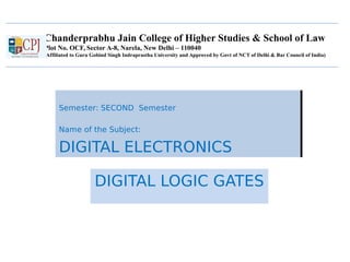
- 1. Chanderprabhu Jain College of Higher Studies & School of Law Plot No. OCF, Sector A-8, Narela, New Delhi – 110040 (Affiliated to Guru Gobind Singh Indraprastha University and Approved by Govt of NCT of Delhi & Bar Council of India) Semester: SECOND Semester Name of the Subject: DIGITAL ELECTRONICS Semester: SECOND Semester Name of the Subject: DIGITAL ELECTRONICS DIGITAL LOGIC GATES
- 2. Overview • Binary logic and Gates • Binary logic Function • Binary logic Operators • Truth Tables • Combinational Logic Circuits • More Logic Gates Chanderprabhu Jain College of Higher Studies & School of Law Plot No. OCF, Sector A-8, Narela, New Delhi – 110040 (Affiliated to Guru Gobind Singh Indraprastha University and Approved by Govt of NCT of Delhi & Bar Council of India)
- 3. Binary Logic • Deals with binary variables that take 2 discrete values (0 and 1), and with logic operations • Three basic logic operations: – AND, OR, NOT • Binary/logic variables are typically represented as letters: A,B,C,…,X,Y,Z Chanderprabhu Jain College of Higher Studies & School of Law Plot No. OCF, Sector A-8, Narela, New Delhi – 110040 (Affiliated to Guru Gobind Singh Indraprastha University and Approved by Govt of NCT of Delhi & Bar Council of India)
- 4. Binary Logic Function F(vars) = expression Example: F(a,b) = a’•b + b’ G(x,y,z) = x•(y+z’) set of binary variables Operators ( +, •, ‘ ) Variables Constants ( 0, 1 ) Groupings (parenthesis) Chanderprabhu Jain College of Higher Studies & School of Law Plot No. OCF, Sector A-8, Narela, New Delhi – 110040 (Affiliated to Guru Gobind Singh Indraprastha University and Approved by Govt of NCT of Delhi & Bar Council of India)
- 5. Basic Logic Operators • AND • OR • NOT • F(a,b) = a•b, F is 1 if and only if a=b=1 • G(a,b) = a+b, G is 1 if either a=1 or b=1 • H(a) = a’, H is 1 if a=0 Binary Unary Chanderprabhu Jain College of Higher Studies & School of Law Plot No. OCF, Sector A-8, Narela, New Delhi – 110040 (Affiliated to Guru Gobind Singh Indraprastha University and Approved by Govt of NCT of Delhi & Bar Council of India)
- 6. Basic Logic Operators (cont.)• 1-bit logic AND resembles binary multiplication: 0 • 0 = 0, 0 • 1 = 0, 1 • 0 = 0, 1 • 1 = 1 • 1-bit logic OR resembles binary addition, except for one operation: 0 + 0 = 0, 0 + 1 = 1, 1 + 0 = 1, 1 + 1 = 1 (≠ 102) Chanderprabhu Jain College of Higher Studies & School of Law Plot No. OCF, Sector A-8, Narela, New Delhi – 110040 (Affiliated to Guru Gobind Singh Indraprastha University and Approved by Govt of NCT of Delhi & Bar Council of India)
- 7. Truth Tables for logic operators Truth table: tabular form that uniguely represents the relationship between the input variables of a function and its output A B F=A•B 0 0 0 0 1 0 1 0 0 1 1 1 2-Input AND A B F=A+B 0 0 0 0 1 1 1 0 1 1 1 1 2-Input OR A F=A’ 0 1 1 0 NOT Chanderprabhu Jain College of Higher Studies & School of Law Plot No. OCF, Sector A-8, Narela, New Delhi – 110040 (Affiliated to Guru Gobind Singh Indraprastha University and Approved by Govt of NCT of Delhi & Bar Council of India)
- 8. Logic Gates • Logic gates are abstractions of electronic circuit components that operate on one or more input signals to produce an output signal. 2-Input AND 2-Input OR NOT (Inverter) A A A B B F G H F = A•B G = A+B H = A’ Chanderprabhu Jain College of Higher Studies & School of Law Plot No. OCF, Sector A-8, Narela, New Delhi – 110040 (Affiliated to Guru Gobind Singh Indraprastha University and Approved by Govt of NCT of Delhi & Bar Council of India)
- 9. Combinational Logic Circuit from Logic Function • Consider function F = A’ + B•C’ + A’•B’ • A combinational logic circuit can be constructed to implement F, by appropriately connecting input signals and logic gates: – Circuit input signals from function variables (A, B, C) – Circuit output signal function output (F) – Logic gates from logic operations A B C F Chanderprabhu Jain College of Higher Studies & School of Law Plot No. OCF, Sector A-8, Narela, New Delhi – 110040 (Affiliated to Guru Gobind Singh Indraprastha University and Approved by Govt of NCT of Delhi & Bar Council of India)
- 10. Combinational Logic Circuit from Logic Function (cont.) • In order to design a cost- effective and efficient circuit, we must minimize the circuit’s size (area) and propagation delay (time required for an input signal change to be observed at the output line) • Observe the truth table of F=A’ + B•C’ + A’•B’ and G=A’ + B•C’ • Truth tables for F and G are identical same function • Use G to implement the logic circuit (less components) A B C F G 0 0 0 1 1 0 0 1 1 1 0 1 0 1 1 0 1 1 1 1 1 0 0 0 0 1 0 1 0 0 1 1 0 1 1 1 1 1 0 0 Chanderprabhu Jain College of Higher Studies & School of Law Plot No. OCF, Sector A-8, Narela, New Delhi – 110040 (Affiliated to Guru Gobind Singh Indraprastha University and Approved by Govt of NCT of Delhi & Bar Council of India)
- 11. More Logic Gates • We can construct any combinational circuit with AND, OR, and NOT gates • Additional logic gates are used for practical reasons Chanderprabhu Jain College of Higher Studies & School of Law Plot No. OCF, Sector A-8, Narela, New Delhi – 110040 (Affiliated to Guru Gobind Singh Indraprastha University and Approved by Govt of NCT of Delhi & Bar Council of India)
- 12. BUFFER, NAND and NOR Chanderprabhu Jain College of Higher Studies & School of Law Plot No. OCF, Sector A-8, Narela, New Delhi – 110040 (Affiliated to Guru Gobind Singh Indraprastha University and Approved by Govt of NCT of Delhi & Bar Council of India)
- 13. NAND Gate • Known as a “universal” gate because ANY digital circuit can be implemented with NAND gates alone. • To prove the above, it suffices to show that AND, OR, and NOT can be implemented using NAND gates only. Chanderprabhu Jain College of Higher Studies & School of Law Plot No. OCF, Sector A-8, Narela, New Delhi – 110040 (Affiliated to Guru Gobind Singh Indraprastha University and Approved by Govt of NCT of Delhi & Bar Council of India)
- 14. Chanderprabhu Jain College of Higher Studies & School of Law Plot No. OCF, Sector A-8, Narela, New Delhi – 110040 (Affiliated to Guru Gobind Singh Indraprastha University and Approved by Govt of NCT of Delhi & Bar Council of India) Semester: SECOND Semester Name of the Subject: DIGITAL ELECTRONICS Semester: SECOND Semester Name of the Subject: DIGITAL ELECTRONICS ARITHMETIC CIRCUITS
- 15. Half Adder With twos complement numbers, addition is sufficient Ai 0 0 1 1 Bi 0 1 0 1 Sum 0 1 1 0 Carry 0 0 0 1 Ai Bi 0 1 0 1 0 1 1 0 Sum = Ai Bi + Ai Bi = Ai + Bi Ai Bi 0 1 0 1 0 0 10 Carry = Ai Bi Half-adder Schematic Carry Sum Ai Bi Chanderprabhu Jain College of Higher Studies & School of Law Plot No. OCF, Sector A-8, Narela, New Delhi – 110040 (Affiliated to Guru Gobind Singh Indraprastha University and Approved by Govt of NCT of Delhi & Bar Council of India)
- 16. Full Adder + A3 B3 S3 + A2 B2 S2 + A1 B1 S1 + A0 B0 S0C1C2C3 Cascaded Multi-bit Adder usually interested in adding more than two bits this motivates the need for the full adder Chanderprabhu Jain College of Higher Studies & School of Law Plot No. OCF, Sector A-8, Narela, New Delhi – 110040 (Affiliated to Guru Gobind Singh Indraprastha University and Approved by Govt of NCT of Delhi & Bar Council of India)
- 17. Full Adder A 0 0 0 0 1 1 1 1 B 0 0 1 1 0 0 1 1 CI 0 1 0 1 0 1 0 1 S 0 1 1 0 1 0 0 1 CO 0 0 0 1 0 1 1 1 A B CI 0 1 00 01 11 10 0 1 1 0 1 0 0 1 A B CI 0 1 00 01 11 10 0 0 0 1 0 1 1 1 S CO S = CI xor A xor B CO = B CI + A CI + A B = CI (A + B) + A B Chanderprabhu Jain College of Higher Studies & School of Law Plot No. OCF, Sector A-8, Narela, New Delhi – 110040 (Affiliated to Guru Gobind Singh Indraprastha University and Approved by Govt of NCT of Delhi & Bar Council of India)
- 18. Full Adder/Half Adder A A A B B B CI CI S CO Alternative Implementation: 5 Gates Half Adder A B Half Adder A + B CI A + B + CIS S COCO CI (A + B)A B S CO A B + CI (A xor B) = A B + B CI + A CI Standard Approach: 6 Gates + Chanderprabhu Jain College of Higher Studies & School of Law Plot No. OCF, Sector A-8, Narela, New Delhi – 110040 (Affiliated to Guru Gobind Singh Indraprastha University and Approved by Govt of NCT of Delhi & Bar Council of India)
- 19. Adder/Subtractor A - B = A + (-B) = A + B + 1 A B CO S + CI A B CO S + CI A B CO S + CI A B CO S + CI 0 1 Add/Subtract A3 B3 B3 0 1 A2 B2 B2 0 1 A1 B1 B1 0 1 A0 B0 B0 Sel Sel Sel Sel S3 S2 S1 S0 Overflow Chanderprabhu Jain College of Higher Studies & School of Law Plot No. OCF, Sector A-8, Narela, New Delhi – 110040 (Affiliated to Guru Gobind Singh Indraprastha University and Approved by Govt of NCT of Delhi & Bar Council of India)
- 20. Basic Concept multiplicand multiplier 1101 (13) 1011 (11) 1101 1101 0000 1101 * 10001111 (143) Partial products product of 2 4-bit numbers is an 8-bit number Chanderprabhu Jain College of Higher Studies & School of Law Plot No. OCF, Sector A-8, Narela, New Delhi – 110040 (Affiliated to Guru Gobind Singh Indraprastha University and Approved by Govt of NCT of Delhi & Bar Council of India)
- 21. Partial Product Accumulation A0 B0 A0 B0 A1 B1 A1 B0 A0 B1 A2 B2 A2 B0 A1 B1 A0 B2 A3 B3 A2 B0 A2 B1 A1 B2 A0 B3 A3 B1 A2 B2 A1 B3 A3 B2 A2 B3A3 B3 S6 S5 S4 S3 S2 S1 S0S7 Chanderprabhu Jain College of Higher Studies & School of Law Plot No. OCF, Sector A-8, Narela, New Delhi – 110040 (Affiliated to Guru Gobind Singh Indraprastha University and Approved by Govt of NCT of Delhi & Bar Council of India)
- 22. Partial Product Accumulation A0 B0A1 B0A0 B1A0 B2A1 B1A2 B0A0 B3A 1 B2A2 B1A3 B0A1 B3A 2 B2A3 B1A2 B3A3 B2A3 B3 HA S0S1 HA FA FA S3 FA FA S4 HA FA S2 FA FA S5 FA S6 HA S7 Chanderprabhu Jain College of Higher Studies & School of Law Plot No. OCF, Sector A-8, Narela, New Delhi – 110040 (Affiliated to Guru Gobind Singh Indraprastha University and Approved by Govt of NCT of Delhi & Bar Council of India)
- 23. Case Study: 8 x 8 Multiplier Three-At-A-Time Adder with TTL Components Full Adders (2 per package) Standard ALU configured as 4-bit cascaded adder (with internal carry lookahead) B3 A3 B2 A2 B1 A1 B0 A0 F3 F2 F1 F0 Cn G P Cn+4 74181 + Cn B A Cn+1 S 74183 Cn B A Cn+1 S 74183 Cn B A Cn+1 S 74183 Cn B A Cn+1 S 74183 S 0 S 1 S 2 S 3 A0B0C0A1B1C1A2B2C2A3B3C3
- 24. Chanderprabhu Jain College of Higher Studies & School of Law Plot No. OCF, Sector A-8, Narela, New Delhi – 110040 (Affiliated to Guru Gobind Singh Indraprastha University and Approved by Govt of NCT of Delhi & Bar Council of India) Semester: SECOND Semester Name of the Subject: DIGITAL ELECTRONICS Semester: SECOND Semester Name of the Subject: DIGITAL ELECTRONICS Intro To FLIP-FLOPS
- 25. Combinational Logic •The outputs depend only on the state of the inputs all of the time. Any change in the state of one of the inputs will ripple through the circuit immediately. o Examples of combinational logic are NAND and NOR gates, Inverters, and Buffers. These four logic gates form the basis of almost all combinational logic circuits as well as flip flops. •Circuits that change the state of the output in this manner are also known as asynchronous circuits. o However, not all asynchronous circuits are Chanderprabhu Jain College of Higher Studies & School of Law Plot No. OCF, Sector A-8, Narela, New Delhi – 110040 (Affiliated to Guru Gobind Singh Indraprastha University and Approved by Govt of NCT of Delhi & Bar Council of India)
- 26. Sequential Logic • Has memory; the circuit stores the result of the previous set of inputs. The current output depends on inputs in the past as well as present inputs. o The basic element in sequential logic is the bistable latch or flip-flop, which acts as a memory element for one bit of data. Chanderprabhu Jain College of Higher Studies & School of Law Plot No. OCF, Sector A-8, Narela, New Delhi – 110040 (Affiliated to Guru Gobind Singh Indraprastha University and Approved by Govt of NCT of Delhi & Bar Council of India)
- 27. Clocked Circuits •Most flip-flops are clocked so that the output change state based upon the state of the inputs at precisely determined times. o Usage varies — in this course, ‘flip-flops’ will be used for clocked circuits and ‘latches’ for circuits that are asynchronous. •A common clock used in many flip-flips in one circuit ensures that all parts of a digital system change state at the same time. This is called a synchronous systemChanderprabhu Jain College of Higher Studies & School of Law Plot No. OCF, Sector A-8, Narela, New Delhi – 110040 (Affiliated to Guru Gobind Singh Indraprastha University and Approved by Govt of NCT of Delhi & Bar Council of India)
- 28. Bistable Circuit • At the heart of a bistable circuit is a pair of inverters connected in a loop — with feedback, in other words. It has two stable states. – Without some control, there isn’t a way to force the bistable circuit into one or the other state. Chanderprabhu Jain College of Higher Studies & School of Law Plot No. OCF, Sector A-8, Narela, New Delhi – 110040 (Affiliated to Guru Gobind Singh Indraprastha University and Approved by Govt of NCT of Delhi & Bar Council of India)
- 29. Bistable Circuits •The bistable circuit is used as a ‘bus keeper’ to hold a node at a definite 1 or 0. It is also the heart of a ‘static random access memory’ (SRAM) cell. o Similar operation occurs for any ring composed of an even number of invertors. o What would happen if 3 inverters (or larger odd number) are connected in series? This type of circuit is called a ring oscillator. Check this out in the laboratory or in PSpice! Chanderprabhu Jain College of Higher Studies & School of Law Plot No. OCF, Sector A-8, Narela, New Delhi – 110040 (Affiliated to Guru Gobind Singh Indraprastha University and Approved by Govt of NCT of Delhi & Bar Council of India)
- 30. Core of a Flip-Flop: The set–reset or SR Latch• Acts as a simple memory with two stable states at the two output when S = R = 0 – Q1 and Q2 are the outputs of the S-R latch. – When Q1 is known as Q and Q2 is also called Q’ or (spoken as Q bar), meaning that its value is not Q or the opposite of Q. Q Chanderprabhu Jain College of Higher Studies & School of Law Plot No. OCF, Sector A-8, Narela, New Delhi – 110040 (Affiliated to Guru Gobind Singh Indraprastha University and Approved by Govt of NCT of Delhi & Bar Council of India)
- 31. S-R Latch Acts as a simple memory with two stable states when S = R = 0: • The latch - holds (stores) when S = R = 0 - is set (to 1) by bringing S = 1 with R = 0 - is reset (to 0) or cleared by bringing R = 1 with S = 0 • The condition S = R = 1 must be avoided because it leads to an indeterminate condition, where the output can not be predicted at any one point in time. This can cause a race condition to occur when the inputs change to S = R = 0. Chanderprabhu Jain College of Higher Studies & School of Law Plot No. OCF, Sector A-8, Narela, New Delhi – 110040 (Affiliated to Guru Gobind Singh Indraprastha University and Approved by Govt of NCT of Delhi & Bar Council of India)
- 32. SR Latch with Enable • The S and R inputs only effect the output states when the enable input C is high. – This controls when the latch responds to its inputs. • The latch holds (stores) its value while the enable input is low — latches it! • Any changes in the inputs during the time when enable is high will affect the output immediately: the circuit is said to be transparent. • This circuit still has a major problem: the stored value is indeterminate if S = R = 1 when the clock goes low Chanderprabhu Jain College of Higher Studies & School of Law Plot No. OCF, Sector A-8, Narela, New Delhi – 110040 (Affiliated to Guru Gobind Singh Indraprastha University and Approved by Govt of NCT of Delhi & Bar Council of India)
- 33. Logic Table SR Latch S R Q 0 0 Last Q 0 1 0 1 0 1 1 1 SR Latch with Enable S R E Q 0 0 1 Last Q 0 1 1 0 1 0 1 1 1 1 1 X X 0 Last QChanderprabhu Jain College of Higher Studies & School of Law Plot No. OCF, Sector A-8, Narela, New Delhi – 110040 (Affiliated to Guru Gobind Singh Indraprastha University and Approved by Govt of NCT of Delhi & Bar Council of India)
- 34. D Flip-Flop •The problem with S = R = 1 can be avoided using a common input D as shown above so that . •The output of the latch now: – follows the D input while C = 1 (transparent) – holds its value while C = 0 (Q = last Q when C went low) no matter what happens at the input •This circuit is often called a transparent latch. It can be bought as an integrated circuit, usually with several latches in a package. – The input C may be called control, clock, gate, or enable. RS Chanderprabhu Jain College of Higher Studies & School of Law Plot No. OCF, Sector A-8, Narela, New Delhi – 110040 (Affiliated to Guru Gobind Singh Indraprastha University and Approved by Govt of NCT of Delhi & Bar Council of India)
- 35. Timing Diagrams D Q C Q D C output follows input output remains constant: input ‘latched’ Q D Q C Q D C' output follows input output remains constant: input ‘latched’ Q Chanderprabhu Jain College of Higher Studies & School of Law Plot No. OCF, Sector A-8, Narela, New Delhi – 110040 (Affiliated to Guru Gobind Singh Indraprastha University and Approved by Govt of NCT of Delhi & Bar Council of India)
- 36. Chanderprabhu Jain College of Higher Studies & School of Law Plot No. OCF, Sector A-8, Narela, New Delhi – 110040 (Affiliated to Guru Gobind Singh Indraprastha University and Approved by Govt of NCT of Delhi & Bar Council of India) Semester: SECOND Semester Name of the Subject: DIGITAL ELECTRONICS Semester: SECOND Semester Name of the Subject: DIGITAL ELECTRONICS Intro To FLIP-FLOPS
- 37. [ Figure 5.15a,c from the textbook T Flip-Flop (circuit and graphical symbol)
- 38. A three-bit up-counter [ Figure 5.19 from the textbook
- 39. A three-bit up-counter [ Figure 5.19 from the textbook The first flip-flop changes on the positive edge of the clock
- 40. A three-bit up-counter [ Figure 5.19 from the textbook The first flip-flop changes on the positive edge of the clock The second flip-flop changes on the positive edge of Q0
- 41. A three-bit up-counter [ Figure 5.19 from the textbook The first flip-flop changes on the positive edge of the clock The second flip-flop changes on the positive edge of Q0 The third flip-flop changes on the positive edge of Q1
- 42. A three-bit up-counter [ Figure 5.19 from the textbook T Q QClock T Q Q T Q Q 1 Q0 Q1 Q2 (a) Circuit Clock Q0 Q1 Q2 Count 0 1 2 3 4 5 6 7 0 (b) Timing diagram
- 43. A three-bit up-counter [ Figure 5.19 from the textbook T Q QClock T Q Q T Q Q 1 Q0 Q1 Q2 (a) Circuit Clock Q0 Q1 Q2 Count 0 1 2 3 4 5 6 7 0 (b) Timing diagram The propagation delays get longer
- 44. A three-bit down-counter [ Figure 5.20 from the textbook
- 45. A three-bit down-counter [ Figure 5.20 from the textbook T Q QClock T Q Q T Q Q 1 Q0 Q1 Q2 (a) Circuit Clock Q0 Q1 Q2 Count 0 7 6 5 4 3 2 1 0 (b) Timing diagram
- 47. A four-bit synchronous up-counter [ Figure 5.21 from the textbook
- 48. A four-bit synchronous up-counter [ Figure 5.21 from the textbook The propagation delay through all AND gates combined must not exceed the clock period minus the setup time for the flip-flops
- 49. A four-bit synchronous up-counter [ Figure 5.21 from the textbook T Q QClock T Q Q T Q Q 1 Q0 Q1 Q2 (a) Circuit Clock Q0 Q1 Q2 Count 0 1 2 3 5 9 12 14 0 (b) Timing diagram T Q Q Q3 Q3 4 6 87 10 11 13 15 1
- 50. Derivation of the synchronous up-counter [ Table 5.1 from the textbook ] 0 0 1 1 0 1 0 1 0 1 2 3 0 0 1 0 1 0 4 5 6 1 17 0 0 0 0 1 1 1 1 Clock cycle 0 08 0 Q2 Q1 Q0 Q1changes Q2changes
- 51. Derivation of the synchronous up-counter [ Table 5.1 from the textbook ] 0 0 1 1 0 1 0 1 0 1 2 3 0 0 1 0 1 0 4 5 6 1 17 0 0 0 0 1 1 1 1 Clock cycle 0 08 0 Q2 Q1 Q0 Q1changes Q2changes T0= 1 T1 = Q0 T2 = Q0 Q1
- 52. A four-bit synchronous up-counter [ Figure 5.21 from the textbook T0= 1 T1 = Q0 T2 = Q0 Q1