SlideShare a Scribd company logo
1 of 1
Download to read offline
Design of an Electron Cloud Detector in
a Quadrupole Magnet at CESRTA*
J.P. Sikora†
, S.T. Barrett, M.G. Billing, J.A. Crittenden, K.A. Jones,
Y. Li, T. O'Connell, CLASSE, Ithaca, New York 14853, USA
Abstract
We have designed a detector that measures the electron cloud density in
a quadrupole magnet using two independent techniques. Stripline
electrodes collect electrons which pass through holes in the beam-pipe
wall. The array of small holes in the beam-pipe wall shield the striplines
from the beam-induced electromagnetic pulse. Three striplines cover a
roughly 0.45 radian azimuth near one of the pole tips. The beam-pipe
chamber has also been designed so that microwave measurements of the
electron cloud density can be performed. Beam position monitor style
buttons have been included for excitation and reception of microwaves
and the chamber has been designed so that the resonant microwaves are
confined to be within the 56 cm length of the quadrupole. This paper
provides some details of the design including CST Microwave Studio®
time domain simulation of the stripline detectors and eigenmode
simulation of the TE11
modes in the resonant chamber. The detector is
installed in the Cornell Electron Storage Ring and is part of the test
accelerator program for the study of electron cloud build-up using
electron and positron beams from 2 to 5GeV.
An exploded view of the single stripline detector
CLASSE facilities are operated by Cornell and the Cornell High Energy Synchrotron Source (CHESS) with major support from the National Science Foundation.
*This work is supported by the US National Science Foundation PHY-0734867, PHY-1002467 and the US Department of Energy DE-FC02-08ER41538, DE-SC0006505.
Stripline Design
Microwave Design
Holes in the beam-pipe wall allow electrons to be
collected by the stripline while shielding it from the direct
electromagnetic pulse of the beam.
The dual stripline has holes that are angled to follow the
magnetic field lines of the quadrupole field. Both the single and
dual stripline assemblies are centered on a pole face, but are at
different longitudinal positions.
The array of holes is fabricated in stainless plates by
electrical discharge machining (EDM). The plates are
then welded into slots in the beam-pipe.
CST Microwave Studio®
simulation of the stripline
dimensions gives about 50 ohms
Resonant Microwave Measurement
of Electron Cloud Density
A train of bunches in a storage ring will produce a periodic
electron cloud (EC) density. If the beam-pipe is resonantly
excited with microwaves, the resonant frequency will be
modulated by the EC density. The magnitude of the EC density
can then be measured through the resulting phase modulation
sidebands in the resonant response. In the sketch above, ω is
the drive frequency and ωT
the revolution frequency.
The frequency shift is given by Eq. 1 with ne
the EC density, E the
resonant electric field and V the resonant volume. To measure only
the EC density in the quadrupole field, the microwaves must be
contained in the section of beam-pipe that is within the quadrupole.
Δ ω
ω0
≈
e2
2ε0 me ω0
2
∫V
ne E
2
dV
∫V
E2
dV
(1)
Center (Single) Detector Upper Detector Lower Detector
Time delay reflectometer (TDR) tests of the striplines after the final welds
show an impedance close to 50 ohms for the center and upper detector, but
the lower detector has a short at one end. The vertical scale is 50 mρ/div.
ECLOUD simulation of the EC density just after the passage of a 20-bunch train of 5.3 GeV
positrons with 14 ns spacing shows an increase in the splitting of the cloud near the pole face
as the bunch population is increased from 1.2 x 10¹¹
(left) to 1.3 x 10¹¹
particles/bunch (right).
The green lines represent electron trajectories through the holes of the single stripline detector;
red lines are the trajectories into the dual detector.
+50 V bias
For data taking, the stripline signal is amplified and connected to an oscilloscope.
The round chamber with transitions to quasi-rectangular CESR beam-pipe was
modeled in Autodesk Inventor®
. The model was then imported to CST Microwave
Studio®
for simulation of the TE11
eigenmodes.
Simulation of a chamber with a 89 mm dia. round center section
showed that most TE11
resonances with vertical E extended out into
the CESR beam-pipe.
When the round chamber diameter was increased to 95.5 mm, the lowest
resonances were confined by the transitions to be within the 560 mm length
of the quadrupole magnet. This dimension was used in the final design.
In a bead pull measurement, the shift in resonant frequency is
proportional to the square of the resonant electric field at the location
of the bead. A bead pull measurement was performed on the
fabricated chamber which confirmed the simulation result.
†jps13@cornell.edu
22 mm
The combination of the single and dual striplines gives an effective detector width of 22 mm.
The Electron Detector

More Related Content

What's hot

Optical Properties of Mesoscopic Systems of Coupled Microspheres
Optical Properties of Mesoscopic Systems of Coupled MicrospheresOptical Properties of Mesoscopic Systems of Coupled Microspheres
Optical Properties of Mesoscopic Systems of Coupled MicrospheresShashaanka Ashili
 
Scanning Electron Microscope 2
Scanning Electron Microscope 2Scanning Electron Microscope 2
Scanning Electron Microscope 2Vikas Barnwal
 
PLASMONS: A modern form of super particle waves
PLASMONS: A modern form of super particle wavesPLASMONS: A modern form of super particle waves
PLASMONS: A modern form of super particle wavesDHRUVIN PATEL
 
1.1 Enrichment
1.1 Enrichment1.1 Enrichment
1.1 Enrichmentjrt004
 
EDS in TEM and SEM
EDS in TEM and SEMEDS in TEM and SEM
EDS in TEM and SEMHoang Tien
 
Auger Electron Spectroscopy
Auger Electron SpectroscopyAuger Electron Spectroscopy
Auger Electron Spectroscopyhasanjamal13
 
Energy Dispersive Spectroscopy
Energy Dispersive SpectroscopyEnergy Dispersive Spectroscopy
Energy Dispersive SpectroscopySaad Shaukat
 
EDS softwares INCA and EDAX_EM forum_Yina Guo_May 2016
EDS softwares INCA and EDAX_EM forum_Yina Guo_May 2016EDS softwares INCA and EDAX_EM forum_Yina Guo_May 2016
EDS softwares INCA and EDAX_EM forum_Yina Guo_May 2016YinaGuo
 

What's hot (20)

Mc3421712175
Mc3421712175Mc3421712175
Mc3421712175
 
PLASMONICS
PLASMONICSPLASMONICS
PLASMONICS
 
Plasmonics1
Plasmonics1Plasmonics1
Plasmonics1
 
Optical Properties of Mesoscopic Systems of Coupled Microspheres
Optical Properties of Mesoscopic Systems of Coupled MicrospheresOptical Properties of Mesoscopic Systems of Coupled Microspheres
Optical Properties of Mesoscopic Systems of Coupled Microspheres
 
Tem 1
Tem  1Tem  1
Tem 1
 
Scanning Electron Microscope 2
Scanning Electron Microscope 2Scanning Electron Microscope 2
Scanning Electron Microscope 2
 
PLASMONS: A modern form of super particle waves
PLASMONS: A modern form of super particle wavesPLASMONS: A modern form of super particle waves
PLASMONS: A modern form of super particle waves
 
1.1 Enrichment
1.1 Enrichment1.1 Enrichment
1.1 Enrichment
 
EDS in TEM and SEM
EDS in TEM and SEMEDS in TEM and SEM
EDS in TEM and SEM
 
SEM and TEM
SEM and  TEMSEM and  TEM
SEM and TEM
 
Ipes spectroscopy
Ipes spectroscopyIpes spectroscopy
Ipes spectroscopy
 
Research Poster 2 Dongwei Liu
Research Poster 2 Dongwei LiuResearch Poster 2 Dongwei Liu
Research Poster 2 Dongwei Liu
 
plasmonics pdf
plasmonics pdfplasmonics pdf
plasmonics pdf
 
Auger Electron Spectroscopy
Auger Electron SpectroscopyAuger Electron Spectroscopy
Auger Electron Spectroscopy
 
VSM
VSM VSM
VSM
 
Energy Dispersive Spectroscopy
Energy Dispersive SpectroscopyEnergy Dispersive Spectroscopy
Energy Dispersive Spectroscopy
 
EDS softwares INCA and EDAX_EM forum_Yina Guo_May 2016
EDS softwares INCA and EDAX_EM forum_Yina Guo_May 2016EDS softwares INCA and EDAX_EM forum_Yina Guo_May 2016
EDS softwares INCA and EDAX_EM forum_Yina Guo_May 2016
 
Abstract
AbstractAbstract
Abstract
 
SEM,TEM & AFM
SEM,TEM & AFMSEM,TEM & AFM
SEM,TEM & AFM
 
RBS
RBSRBS
RBS
 

Similar to WEPG35_poster

Transmission Electron Microscopy (TEM)
Transmission Electron Microscopy (TEM) Transmission Electron Microscopy (TEM)
Transmission Electron Microscopy (TEM) Zohaib HUSSAIN
 
Electron Beam Lithography review paper - EE541 Dublin City University
Electron Beam Lithography review paper - EE541 Dublin City UniversityElectron Beam Lithography review paper - EE541 Dublin City University
Electron Beam Lithography review paper - EE541 Dublin City UniversityRay Tyndall
 
Nenopartical optical sensors
Nenopartical optical sensorsNenopartical optical sensors
Nenopartical optical sensorsRam Niwas Bajiya
 
Kinetics of X-ray conductivity for an ideal wide-gap semiconductor irradiated...
Kinetics of X-ray conductivity for an ideal wide-gap semiconductor irradiated...Kinetics of X-ray conductivity for an ideal wide-gap semiconductor irradiated...
Kinetics of X-ray conductivity for an ideal wide-gap semiconductor irradiated...Andrii Sofiienko
 
cathode ray oscilloscope
cathode ray oscilloscopecathode ray oscilloscope
cathode ray oscilloscopehajahrokiah
 
Performance analysis of a monopole antenna with fluorescent tubes at 4.9 g hz...
Performance analysis of a monopole antenna with fluorescent tubes at 4.9 g hz...Performance analysis of a monopole antenna with fluorescent tubes at 4.9 g hz...
Performance analysis of a monopole antenna with fluorescent tubes at 4.9 g hz...Alexander Decker
 
SINGLE ELECTRON TRANSISTOR: APPLICATIONS & PROBLEMS
SINGLE ELECTRON TRANSISTOR: APPLICATIONS & PROBLEMSSINGLE ELECTRON TRANSISTOR: APPLICATIONS & PROBLEMS
SINGLE ELECTRON TRANSISTOR: APPLICATIONS & PROBLEMSVLSICS Design
 
Single Electron Transistor: Applications & Problems
Single Electron Transistor: Applications & Problems  Single Electron Transistor: Applications & Problems
Single Electron Transistor: Applications & Problems VLSICS Design
 
322253456-NANOELECTRONICS-ppt of engineering
322253456-NANOELECTRONICS-ppt of engineering322253456-NANOELECTRONICS-ppt of engineering
322253456-NANOELECTRONICS-ppt of engineeringt24042567
 
Electromagnetic waves
Electromagnetic wavesElectromagnetic waves
Electromagnetic wavesharshbharti6
 
Measurement of energy loss of light ions using silicon surface barrier detector
Measurement of energy loss of light ions using silicon surface barrier detectorMeasurement of energy loss of light ions using silicon surface barrier detector
Measurement of energy loss of light ions using silicon surface barrier detectoreSAT Publishing House
 
Electron Spin Resonance Spectroscopy by arju
Electron Spin Resonance Spectroscopy by arjuElectron Spin Resonance Spectroscopy by arju
Electron Spin Resonance Spectroscopy by arjuArjun kumar
 
ELECTRON MICROSCOPY (TEM & SEM)
ELECTRON MICROSCOPY (TEM & SEM)ELECTRON MICROSCOPY (TEM & SEM)
ELECTRON MICROSCOPY (TEM & SEM)ADITYA ARYA
 
Andrii Sofiienko - Electron range evaluation and X-ray conversion optimizatio...
Andrii Sofiienko - Electron range evaluation and X-ray conversion optimizatio...Andrii Sofiienko - Electron range evaluation and X-ray conversion optimizatio...
Andrii Sofiienko - Electron range evaluation and X-ray conversion optimizatio...Andrii Sofiienko
 

Similar to WEPG35_poster (20)

Microwave advancement
Microwave advancementMicrowave advancement
Microwave advancement
 
Transmission Electron Microscopy (TEM)
Transmission Electron Microscopy (TEM) Transmission Electron Microscopy (TEM)
Transmission Electron Microscopy (TEM)
 
Scanning Electron Microscope
Scanning Electron MicroscopeScanning Electron Microscope
Scanning Electron Microscope
 
Electron Beam Lithography review paper - EE541 Dublin City University
Electron Beam Lithography review paper - EE541 Dublin City UniversityElectron Beam Lithography review paper - EE541 Dublin City University
Electron Beam Lithography review paper - EE541 Dublin City University
 
Nenopartical optical sensors
Nenopartical optical sensorsNenopartical optical sensors
Nenopartical optical sensors
 
Kinetics of X-ray conductivity for an ideal wide-gap semiconductor irradiated...
Kinetics of X-ray conductivity for an ideal wide-gap semiconductor irradiated...Kinetics of X-ray conductivity for an ideal wide-gap semiconductor irradiated...
Kinetics of X-ray conductivity for an ideal wide-gap semiconductor irradiated...
 
cathode ray oscilloscope
cathode ray oscilloscopecathode ray oscilloscope
cathode ray oscilloscope
 
NANOELECTRONICS-ppt.ppt
NANOELECTRONICS-ppt.pptNANOELECTRONICS-ppt.ppt
NANOELECTRONICS-ppt.ppt
 
Performance analysis of a monopole antenna with fluorescent tubes at 4.9 g hz...
Performance analysis of a monopole antenna with fluorescent tubes at 4.9 g hz...Performance analysis of a monopole antenna with fluorescent tubes at 4.9 g hz...
Performance analysis of a monopole antenna with fluorescent tubes at 4.9 g hz...
 
SINGLE ELECTRON TRANSISTOR: APPLICATIONS & PROBLEMS
SINGLE ELECTRON TRANSISTOR: APPLICATIONS & PROBLEMSSINGLE ELECTRON TRANSISTOR: APPLICATIONS & PROBLEMS
SINGLE ELECTRON TRANSISTOR: APPLICATIONS & PROBLEMS
 
Single Electron Transistor: Applications & Problems
Single Electron Transistor: Applications & Problems  Single Electron Transistor: Applications & Problems
Single Electron Transistor: Applications & Problems
 
322253456-NANOELECTRONICS-ppt of engineering
322253456-NANOELECTRONICS-ppt of engineering322253456-NANOELECTRONICS-ppt of engineering
322253456-NANOELECTRONICS-ppt of engineering
 
valentinuzzi_paper
valentinuzzi_papervalentinuzzi_paper
valentinuzzi_paper
 
Search for Neutron Electric Dipole Moment
Search for Neutron Electric Dipole MomentSearch for Neutron Electric Dipole Moment
Search for Neutron Electric Dipole Moment
 
Electromagnetic waves
Electromagnetic wavesElectromagnetic waves
Electromagnetic waves
 
Measurement of energy loss of light ions using silicon surface barrier detector
Measurement of energy loss of light ions using silicon surface barrier detectorMeasurement of energy loss of light ions using silicon surface barrier detector
Measurement of energy loss of light ions using silicon surface barrier detector
 
Electron Spin Resonance Spectroscopy by arju
Electron Spin Resonance Spectroscopy by arjuElectron Spin Resonance Spectroscopy by arju
Electron Spin Resonance Spectroscopy by arju
 
s41566-021-00813-y.pdf
s41566-021-00813-y.pdfs41566-021-00813-y.pdf
s41566-021-00813-y.pdf
 
ELECTRON MICROSCOPY (TEM & SEM)
ELECTRON MICROSCOPY (TEM & SEM)ELECTRON MICROSCOPY (TEM & SEM)
ELECTRON MICROSCOPY (TEM & SEM)
 
Andrii Sofiienko - Electron range evaluation and X-ray conversion optimizatio...
Andrii Sofiienko - Electron range evaluation and X-ray conversion optimizatio...Andrii Sofiienko - Electron range evaluation and X-ray conversion optimizatio...
Andrii Sofiienko - Electron range evaluation and X-ray conversion optimizatio...
 

WEPG35_poster

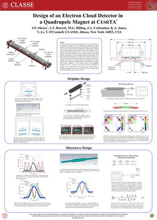
  • 1. Design of an Electron Cloud Detector in a Quadrupole Magnet at CESRTA* J.P. Sikora† , S.T. Barrett, M.G. Billing, J.A. Crittenden, K.A. Jones, Y. Li, T. O'Connell, CLASSE, Ithaca, New York 14853, USA Abstract We have designed a detector that measures the electron cloud density in a quadrupole magnet using two independent techniques. Stripline electrodes collect electrons which pass through holes in the beam-pipe wall. The array of small holes in the beam-pipe wall shield the striplines from the beam-induced electromagnetic pulse. Three striplines cover a roughly 0.45 radian azimuth near one of the pole tips. The beam-pipe chamber has also been designed so that microwave measurements of the electron cloud density can be performed. Beam position monitor style buttons have been included for excitation and reception of microwaves and the chamber has been designed so that the resonant microwaves are confined to be within the 56 cm length of the quadrupole. This paper provides some details of the design including CST Microwave Studio® time domain simulation of the stripline detectors and eigenmode simulation of the TE11 modes in the resonant chamber. The detector is installed in the Cornell Electron Storage Ring and is part of the test accelerator program for the study of electron cloud build-up using electron and positron beams from 2 to 5GeV. An exploded view of the single stripline detector CLASSE facilities are operated by Cornell and the Cornell High Energy Synchrotron Source (CHESS) with major support from the National Science Foundation. *This work is supported by the US National Science Foundation PHY-0734867, PHY-1002467 and the US Department of Energy DE-FC02-08ER41538, DE-SC0006505. Stripline Design Microwave Design Holes in the beam-pipe wall allow electrons to be collected by the stripline while shielding it from the direct electromagnetic pulse of the beam. The dual stripline has holes that are angled to follow the magnetic field lines of the quadrupole field. Both the single and dual stripline assemblies are centered on a pole face, but are at different longitudinal positions. The array of holes is fabricated in stainless plates by electrical discharge machining (EDM). The plates are then welded into slots in the beam-pipe. CST Microwave Studio® simulation of the stripline dimensions gives about 50 ohms Resonant Microwave Measurement of Electron Cloud Density A train of bunches in a storage ring will produce a periodic electron cloud (EC) density. If the beam-pipe is resonantly excited with microwaves, the resonant frequency will be modulated by the EC density. The magnitude of the EC density can then be measured through the resulting phase modulation sidebands in the resonant response. In the sketch above, ω is the drive frequency and ωT the revolution frequency. The frequency shift is given by Eq. 1 with ne the EC density, E the resonant electric field and V the resonant volume. To measure only the EC density in the quadrupole field, the microwaves must be contained in the section of beam-pipe that is within the quadrupole. Δ ω ω0 ≈ e2 2ε0 me ω0 2 ∫V ne E 2 dV ∫V E2 dV (1) Center (Single) Detector Upper Detector Lower Detector Time delay reflectometer (TDR) tests of the striplines after the final welds show an impedance close to 50 ohms for the center and upper detector, but the lower detector has a short at one end. The vertical scale is 50 mρ/div. ECLOUD simulation of the EC density just after the passage of a 20-bunch train of 5.3 GeV positrons with 14 ns spacing shows an increase in the splitting of the cloud near the pole face as the bunch population is increased from 1.2 x 10¹¹ (left) to 1.3 x 10¹¹ particles/bunch (right). The green lines represent electron trajectories through the holes of the single stripline detector; red lines are the trajectories into the dual detector. +50 V bias For data taking, the stripline signal is amplified and connected to an oscilloscope. The round chamber with transitions to quasi-rectangular CESR beam-pipe was modeled in Autodesk Inventor® . The model was then imported to CST Microwave Studio® for simulation of the TE11 eigenmodes. Simulation of a chamber with a 89 mm dia. round center section showed that most TE11 resonances with vertical E extended out into the CESR beam-pipe. When the round chamber diameter was increased to 95.5 mm, the lowest resonances were confined by the transitions to be within the 560 mm length of the quadrupole magnet. This dimension was used in the final design. In a bead pull measurement, the shift in resonant frequency is proportional to the square of the resonant electric field at the location of the bead. A bead pull measurement was performed on the fabricated chamber which confirmed the simulation result. †jps13@cornell.edu 22 mm The combination of the single and dual striplines gives an effective detector width of 22 mm. The Electron Detector