SlideShare a Scribd company logo
1 of 26
EET 4110 SENIOR PROJECT II
__________________________________________________________
DIGITAL ANALOG AUDIO SYNTHESIZER
Ryan Halgren
Shaun Weston
Mindaugas Sanko
Spring 2015
Metropolitan State University of Denver
1 | P a g e - S y n t h e s i z e r
TABLE OF CONTENTS
Executive Summary ..............................................................................................................................2-6
Introduction ...........................................................................................................................................2
Project goal ........................................................................................................................................ 2-3
Problems ................................................................................................................................................3
How it works ...................................................................................................................................... 3-4
Code .......................................................................................................................................................5
Circuits .............................................................................................................................................. 5-6
Conclusion .............................................................................................................................................6
Project Costs ............................................................................................................................................7
Project Plan .............................................................................................................................................8
Appendix ..................................................................................................................................................9
Arduino Code .................................................................................................................................. 9-12
Circuit Details and schematics ...................................................................................................... 12-18
Build and Assembly Pictures ......................................................................................................... 22-24
Resources ...............................................................................................................................................25
Data sheet links .....................................................................................................................................26
Executive Summary
2 | P a g e - S y n t h e s i z e r
Introduction
A synthesizer is an electronic musical instrument that creates musical tones by generating electronic
signals. The generated waveforms can be converted into audible sound using a speaker or headphones.
Synthesizers can either imitate other instruments or generate new timbres that can only be made via
electronic circuitry. There are various methods to generate the signal and various methods to control the
signal as well. The main components of a synthesizer and their purpose are listed below:
1. The Oscillators, which generate the tones.
2. The LFO (Low Frequency Oscillator), which usually modulates either the frequency or gain of
the waveform generated by the oscillators.
3. The Filter, which emphasizes and/or removes certain frequencies.
4. The Envelope Generator, which controls changes in frequency or gain over the duration of the
note.
5. The Amplifier, which controls the overall gain of the synthesizer.
Today nearly all popular music involves a synthesizer and much of it uses the synthesizer as the lead
instrument or as the only instruments. Most genres of music preferred by the younger generations use
synthesizers as the main instrument and they have become the tool of choice for aspiring musicians.
Project goal
The purpose of this project was to build an affordable audio synthesizer that is composed of both
digital and analog circuits. As electrical engineering students we need to be viable in both the digital
and the analog curriculum. With the synthesizer, there are multiple ways in which the analog and
digital aspects can be implemented. For the digital side, we used a reprogrammable microcontroller to
generate the sound waveforms. Using code to design our signals allows for the type of synthesis and
the signals generated by the oscillators to be changed. From the digitally generated analog output of the
microcontroller, the waveform is sent through a series of analog circuits to modulate or augment the
waveform. These circuits include: Low Frequency Oscillator, State Variable Filter, Envelope Generator,
Ring Modulator, Voltage Controlled Amplifier and Bass Control. The signal will then be output to an
audio jack so it can be played through a speakers for the user to hear.
Key aspects that we aimed for in project proposal:
Affordability:
o We were able to stay in budget with spending under $175. We were able to accomplish
building a synthesizer design that is much more affordable to own or to build yourself.
Reprogrammable:
o We were able to use a microcontroller to provide the oscillations. The synthesizer is be
programmable, but the output pin need to be re-wired for some of the different kinds of
synthesis code. This makes it more user friendly for engineers than for the average user.
Customized for the user:
o The microcontroller can be reprogrammed and customized with a small amount of
rewiring. The analog circuits are fixed, but there is room in the enclosure for more
circuits and extra connection pins soldered onto the current circuit boards so that
3 | P a g e - S y n t h e s i z e r
additional modulation circuits can be connected in the future. Also it can take an
external input signal from another synthesizer or instrument and modulate its sound with
the LFO, Filters etc.
Problems
The most difficult tasks and our biggest problem was interfacing the keyboard with the microcontroller
and ensuring that we were able to read all of the keys correctly with the number of analog read inputs
on available. We did not realize when we proposed this project how difficult it was to create a piano
style keyboard to control an electronic musical instrument. For now we have a potentiometer knob to
turn to different positions to control the note.
We wanted to use the Arduino Due for our microcontroller because It has a very high sampling rate,
512kbs of programming memory, a ton of ports and has a built in analog to digital converter so it can
generate a sound with code and give an actual analog output of that function. However, we
encountered issues with the Due that we did not foresee. We wanted the Due to allow frequency
changes when a note was being pressed, but the Due does not allow frequency changes in the input pins
and have a fixed value for each pin. This made us fall behind in building the key interface. To fix this
issue, we decided to go with an external keyboard known as the Midi keyboard. We were not able to
attach it for the presentation since we needed a part that has not arrived yet in order to attach a midi
keyboard. This would have allowed us to have a keyboard interface, but it would be an external plug in
instead of being attached with the synthesizer.
How it Works
The block diagram for our synthesizer design in Figure 1 below shows the parts of the synth and how
the circuits interconnect. The audio signal flow is shown by the black arrows and the orange arrows
represent control voltage signals.
For what we were able to get working by the end of the semester we simply have a potentiometer
connected to the 5 volt pin of the micro controller for our keyboard control voltage to determine the
note being played. From the Microcontroller output pin the signal goes through a basic Audio Amplifier
circuit with a small gain to boost the signal so that it will work correctly with the analog circuits. From
there it goes to the Ring Modulator, which is how the control voltage waveform from the Low
Frequency Oscillator modulates the sound. The LFO waveform is a sinusoidal signal with variable
shape and speed which controls the volume of the signal through amplitude modulation. After the Ring
Modulator the signal goes to the first Voltage Controlled Amplifier to allow the Envelope Generator to
shape and control the gain of the signal. The Envelope Generator is triggered by a voltage pulse from
the micro-controller or from a manual push button connected to the positive voltage rail. Once
triggered the Envelope Generator shapes the a voltage signal to have a rise and fall to it, instead of an
instantaneous change from low to high and high to low. The Voltage Controlled Amplifier allows this
voltage shape to control the rise and fall of the volume of the signal for each time the E.G. is triggered.
4 | P a g e - S y n t h e s i z e r
Figure 1. Synthesizer Flow Chart
The next stage is the State Variable Filter, which allows the user to select and filter out certain
frequencies through High Pass, Low Pass and Band Pass filters. The Bass Volume Control circuit is
fairly simple, it just cuts or boosts the low frequencies (~300Hz and under). The final stage is another
Voltage Controlled Amplifier which reads the voltage through a potentiometer to control the overall
gain of the synthesizer sound.
Code (see Appendix for code and details)
The microcontroller can be reprogrammed with different types of oscillators but the output pins of the
micro controller have to be rewired when the code is changed. We have two versions of oscillator code.
One uses the Pulse Width Modulation output and can be used with most Arduino types. The second is
only compatible with the Arduino Due and uses the digital to analog converter output to generate
programmed waveforms.
Circuits (see Appendix for circuit details and schematics)
Audio Amplifier:
The Audio Amplifier circuit that we decided to use is a very simple amplifier with a gain of only 5 to
try to avoid noise. The design is based on the schematic given on the data sheet an IC. We changed the
value of select passive components to get the gain we desired.
5 | P a g e - S y n t h e s i z e r
Low Frequency Oscillator:
The LFO signal is used as a periodic control to modulate other component’s value. Our LFO modulates
the amplitude of the signal via a four quadrant multiplier (ring modulator). Our LFO design has
multiple waveform outputs to select from including square, saw/triangle, pulse and parabolic. The three
adjustable parameters are speed, shape and mix. The speed is variable from 1Hz to 33Hz.
Ring Modulator:
Allows the Low Frequency Oscillator to control the amplitude of the signal through amplitude
modulation. We used a four quadrant multiplier rather than a two quadrant to eliminate the bleed
through of the LFO into the audio signal. This way the LFO signal is not heard, just the effect of the
LFO on the audio signal is heard.
Envelope generator:
The Envelope Generator is used to help shape the sound, a rise and fall in volume, of each note. The
general form of an envelope filter is an ADSR (Attack, Decay, Sustain, Release). This helps control the
time it takes for the note to rise to its peak volume, how long it will remain at its peak and how long it
will take to return to zero volume once the note is released. Our E.G. design implements the standard
ADSR form and can be triggered manually by a button for use with a continuous signal.
 Attack time is the time taken for initial run-up of level from nil to peak, beginning when the key is
first pressed.
 Decay time is the time taken for the subsequent run down from the attack level to the designated
sustain level.
 Sustain level is the level during the main sequence of the sound's duration, until the key is
released.
 Release time is the time taken for the level to decay from the sustain level to zero after the key is
released (2).
Voltage Controlled Amplifier:
The VCA allows a voltage (whether DC or AC signal) to control the gain of the signal being passed
through the amplifier. The effect is a similar sound to the Ring Mod and uses the same
transconductance amplifier input to control the signal. For our first VCA the E.G. creates the shaped
voltage ‘pulse’ to change the volume each time it is triggered. Our second VCA uses a variable DC
voltage to control the volume of the signal.
Filters:
The Type of filter that we decided to use for our synthesizer is a State Variable Filter. It is a cascaded
system which simultaneously outputs a High-Pass, Low-Pass and Band-Pass response using active
filters. We chose this type of design because it allows the operator to rather easily switch between filter
types. The typical design uses three or more operational amplifiers with a summing amplifier and two
integrators. The two resistors in the integrators must remain equal for the filters to vary the cutoff
frequencies in unison while maintaining a stable phase response. This is a very flexible system because
a second order response can be achieved with the HP and LP or a high gain can be achieved by the BP,
depending on the Q value. The cutoff frequency and Q value-(inverse of damping coefficient) are
6 | P a g e - S y n t h e s i z e r
adjustable via two potentiometers. In musical terms adjustable Q value of a filter is known as resonance
of the filter.
Bass Volume Control:
The Bass Volume Control is a frequency selective circuit that give a positive or negative gain in
decibels (boost or cut) at frequencies of 300Hz or less. This controls the bass range of frequencies
without having any effect of the high or treble frequencies.
Power Supply:
We used a +15 volt DC power supply that takes the standard 120v @ 60Hz. We used some 12 volt
regulators to lower the output to +12 volts. We also had to add a load to the 5 volt output of the power
supply to draw current from the +15 volt outputs.
Keyboard & box enclosure: (see Appendix for circuit details)
The box enclosure for the synthesizer is made of oak and plywood. The wood is stained and finished
for a good look and feel. The 15 volt power supply mounted securely inside the wood enclosure with
the plug and switch exposed. The box has rubber feet screwed to the bottom so that it will sit securely
on any surface. 5/8 inch standoff were used to support the circuit boards inside the enclosure.
Conclusion
In completing this project we were able to meet all of the goals we set for ourselves in our senior 1
proposal except for the keyboard interface. We were able to build a reprogrammable musical
synthesizer with a digital oscillator and analog modulation circuits. We stayed under our predicted
budget and built a synthesizer with customizable features that is less than half the cost of any
synthesizer on the market.
As electrical engineering students, it is critical for us to know analog and digital circuits and how they
are inter connected. An audio synthesizer is an excellent project for students to gain experience
applying their knowledge of both circuit types. This project had us programming, designing analog
circuits, building circuits and soldering, building an enclosure box and interfacing with a
microcontroller. The variety, difficulty and amount of work made this project a great challenge.
Because this was a challenging project, we think it was one of the best learning experience of our
academic career. It was incredibly fun designing this synthesizer and we will be continuing to write
new versions of oscillator code and design additional circuits.
7 | P a g e - S y n t h e s i z e r
Project Costs
Parts Quantity Cost per Part Total
LM13700 OTA 2 $2.00 $4.00
TL072 dual op-amp 7 $0.30 $2.10
TL074 quad op-amp 1 $0.40 $0.40
BC547 NPN transistor 5 $0.10 $0.50
7555 Timer 1 $0.45 $0.45
Capacitors (various values) 15 $0.30 $4.50
10K pot linear 2 $1.55 $3.10
100k pot Linear 3 $1.55 $4.65
50k pot linear 1 $1.55 $1.55
500k pot linear 1 $1.00 $1.00
10k pot Logarithmic 5 $0.50 $2.50
100k pot Logarithmic 2 $1.00 $2.00
1M pot Logarithmic 3 $1.00 $3.00
dual gang 10k pot Logarithmic 1 $2.50 $2.50
Resistors (various values) 52 $0.10 $5.20
1/4 inch Audio Jack 1 $2.00 $2.00
7812, 7912 (voltage Regulators) 3 $0.50 $1.50
Switches 3 $1.50 $4.50
Buttons 2 $1.50 $3.00
Ferrite Beads 2 $0.10 $0.20
4n35 Optocoupler 1 $0.50 $0.50
PCB's 2 $8.00 $16.00
+15 volt Power Supply 1 $5.00 $5.00
Arduino Due 1 $50.00 $50.00
Programming Cable 1 $10.00 $10.00
Knobs 15 $1.00 $15.00
1N4148 Diodes 8 $0.10 $0.80
Wires & Solder - $5.00 $5.00
Midi Jack 1 $4.00 $4.00
Rubber Feet 4 $0.50 $2.00
Standoffs 10 $0.20 $2.00
Wood Screws 16 $0.15 $2.40
Wood - $7.00 $7.00
Stain - $4.00 $4.00
Glue - $2.00 $2.00
TOTAL: $174.35
Figure 2. Table of part costs
8 | P a g e - S y n t h e s i z e r
Senoir Project Plan
(Above shows the original project plan, below is the actual time line)
Figure 3. Project Plan vs. Project Outcome
9 | P a g e - S y n t h e s i z e r
Appendix
Synth Basics:
The possible waveform synthesis techniques that our design is capable of are:
 Additive synthesis
 Wavetable synthesis
 Sample-based synthesis
 Pulse width modulation synthesis
Development of the microcontroller:
Figure 4. Arduino Due Microcontroller
We currently have two types of code (two types of synthesis) to load onto the Arduino to create the
oscillators. The first version uses C code based on the open-source code for the Auduino (audio-
Arduino) project. The code we found uses grain frequency changes through Pulse Width Modulation to
generate the sound and only uses 1 input pin to read pitch varied by a potentiometer. The sound is
generated by the PWM output of the micro controller. We plan to build off of this code to allow a midi-
controller to be read by the microcontroller to determine the note rather than a potentiometer.
For the second version of the code we wanted to use the Digital to Analog convert output of the
Arduino Due to produce an oscillator. This code produces four different types of oscillator waveforms:
sine wave, square wave, triangle wave and saw tooth wave. The way we constructed this is by first
having a mapped full cycle of each wave. Once we have it mapped out, there is nothing more than
putting it into the Due’s digital to analog convertor to get the output of each wave. The full code is
shown below of how each waveform is getting mapped out, getting selected, and how it is being
outputted.
Code:
PWM Code Preview:
// Analog in 0: Grain 1 pitch
// Analog in 1: Grain 2 decay
// Analog in 2: Grain 1 decay
// Analog in 3: Grain 2 pitch
// Analog in 4: Grain repetition frequency
#include <avr/io.h>
#include <avr/interrupt.h>
10 | P a g e - S y n t h e s i z e r
uint16_t syncPhaseAcc;
uint16_t syncPhaseInc;
uint16_t grainPhaseAcc;
uint16_t grainPhaseInc;
uint16_t grainAmp;
uint8_t grainDecay;
uint16_t grain2PhaseAcc;
uint16_t grain2PhaseInc;
uint16_t grain2Amp;
uint8_t grain2Decay;
// Map Analogue channels
#define SYNC_CONTROL (4)
#define GRAIN_FREQ_CONTROL (0)
#define GRAIN_DECAY_CONTROL (2)
#define GRAIN2_FREQ_CONTROL (3)
#define GRAIN2_DECAY_CONTROL (1)
uint16_t mapPentatonic(uint16_t input) { //code has mapped out note scales that are not included in this code preview
uint8_t value = (1023-input) / (1024/53);
return (pentatonicTable[value]);
}
void audioOn() {
#if defined(__AVR_ATmega8__)
// ATmega8 has different registers
TCCR2 = _BV(WGM20) | _BV(COM21) | _BV(CS20);
TIMSK = _BV(TOIE2);
#elif defined(__AVR_ATmega1280__)
TCCR3A = _BV(COM3C1) | _BV(WGM30);
TCCR3B = _BV(CS30);
TIMSK3 = _BV(TOIE3);
#else
// Set up PWM to 31.25kHz, phase accurate
TCCR2A = _BV(COM2B1) | _BV(WGM20);
TCCR2B = _BV(CS20);
TIMSK2 = _BV(TOIE2);
#endif
// Stepped pentatonic mapping: D, E, G, A, B
syncPhaseInc =mapPentatonic(analogRead(SYNC_CONTROL));
grainPhaseInc = mapPhaseInc(analogRead(GRAIN_FREQ_CONTROL)) / 2;
grainDecay = analogRead(GRAIN_DECAY_CONTROL) / 8;
grain2PhaseInc = mapPhaseInc(analogRead(GRAIN2_FREQ_CONTROL)) / 2;
grain2Decay = analogRead(GRAIN2_DECAY_CONTROL) / 4;
}
SIGNAL(PWM_INTERRUPT)
{
uint8_t value;
uint16_t output;
syncPhaseAcc +=syncPhaseInc;
if (syncPhaseAcc < syncPhaseInc){
// Time to start the next grain
grainPhaseAcc = 0;
grainAmp = 0x7fff;
grain2PhaseAcc = 0;
11 | P a g e - S y n t h e s i z e r
grain2Amp = 0x7fff;
LED_PORT ^= 1 << LED_BIT; // Faster than using digitalWrite
}
DAC code:
#include "Waveforms.h"
#include "Arduino.h"
#define oneHzSample 1000000/maxSamplesNum // sample for the 1Hz signal expressed in microseconds
const int wavebutton = 2, octane = 9, key1 = 3, key2 = 4, key3 = 5, key4 = 6, key5 = 7;
volatile int wave1 = 0, octaneChange = 0;
int keyfound = 0, i = 0;
int sample;
void setup()
{
analogWriteResolution(12); // set the analog output resolution to 12 bit (4096 levels)
analogReadResolution(12); // set the analog input resolution to 12 bit
//pinMode (key1, INPUT);
//pinMode (key2, INPUT);
//pinMode (key3, INPUT);
//pinMode (key4, INPUT);
//pinMode (key5, INPUT);
attachInterrupt(wavebutton,wave1Select, RISING); // Interrupt attached to the button connected to pin 3
//attachInterrupt(octane,OctaneSelect, RISING);
}
void loop(){
//while(digitalRead(key1) == HIGH || digitalRead(key2) == HIGH || digitalRead(key3) == HIGH || digitalRead(key4) ==
HIGH || digitalRead(key5) == HIGH )//{
// Read the the potentiometer and map the value between the maximum and the minimum sample available
// 1 Hz is the minimum freq for the complete wave
// 170 Hz is the maximum freq for the complete wave. Measured considering the loop and the analogRead() time
sample = map(analogRead(A0), 0, 4095, 0, oneHzSample);
sample = constrain(sample, 0, oneHzSample);
analogWrite(DAC1, waveformsTable[wave1][i]); // write the selected waveform on DAC1
i++;
if(i == maxSamplesNum) // Reset the counter to repeat the wave
i = 0;
delayMicroseconds(sample); // Hold the sample value for the sample time
//}}
// function hooked to the interrupt on digital pin 3
void wave1Select() {
wave1++;
if(wave1 == 4)
wave1 = 0;}
Waveforms file:
#ifndef _Waveforms_h_
#define _Waveforms_h_
#define maxWaveform 4
#define maxSamplesNum 120
static int waveformsTable[maxWaveform][maxSamplesNum] = {
// Sin wave
{
0x7ff, 0x86a, 0x8d5, 0x93f, 0x9a9, 0xa11, 0xa78, 0xadd, 0xb40, 0xba1,
12 | P a g e - S y n t h e s i z e r
0xbff, 0xc5a, 0xcb2, 0xd08, 0xd59, 0xda7, 0xdf1, 0xe36, 0xe77, 0xeb4,
0xeec, 0xf1f, 0xf4d, 0xf77, 0xf9a, 0xfb9, 0xfd2, 0xfe5, 0xff3, 0xffc,
0xfff, 0xffc, 0xff3, 0xfe5, 0xfd2, 0xfb9, 0xf9a, 0xf77, 0xf4d, 0xf1f,
0xeec, 0xeb4, 0xe77, 0xe36, 0xdf1, 0xda7, 0xd59, 0xd08, 0xcb2, 0xc5a,
0xbff, 0xba1, 0xb40, 0xadd, 0xa78, 0xa11, 0x9a9, 0x93f, 0x8d5, 0x86a,
0x7ff, 0x794, 0x729, 0x6bf, 0x655, 0x5ed, 0x586, 0x521, 0x4be, 0x45d,
0x3ff, 0x3a4, 0x34c, 0x2f6, 0x2a5, 0x257, 0x20d, 0x1c8, 0x187, 0x14a,
0x112, 0xdf, 0xb1, 0x87, 0x64, 0x45, 0x2c, 0x19, 0xb, 0x2,
0x0, 0x2, 0xb, 0x19, 0x2c, 0x45, 0x64, 0x87, 0xb1, 0xdf,
0x112, 0x14a, 0x187, 0x1c8, 0x20d, 0x257, 0x2a5, 0x2f6, 0x34c, 0x3a4,
0x3ff, 0x45d, 0x4be, 0x521, 0x586, 0x5ed, 0x655, 0x6bf, 0x729, 0x794
},
// Triangular wave
{
0x44, 0x88, 0xcc, 0x110, 0x154, 0x198, 0x1dc, 0x220, 0x264, 0x2a8,
0x2ec, 0x330, 0x374, 0x3b8, 0x3fc, 0x440, 0x484, 0x4c8, 0x50c, 0x550,
0x594, 0x5d8, 0x61c, 0x660, 0x6a4, 0x6e8, 0x72c, 0x770, 0x7b4, 0x7f8,
0x83c, 0x880, 0x8c4, 0x908, 0x94c, 0x990, 0x9d4, 0xa18, 0xa5c, 0xaa0,
0xae4, 0xb28, 0xb6c, 0xbb0, 0xbf4, 0xc38, 0xc7c, 0xcc0, 0xd04, 0xd48,
0xd8c, 0xdd0, 0xe14, 0xe58, 0xe9c, 0xee0, 0xf24, 0xf68, 0xfac, 0xff0,
0xfac, 0xf68, 0xf24, 0xee0, 0xe9c, 0xe58, 0xe14, 0xdd0, 0xd8c, 0xd48,
0xd04, 0xcc0, 0xc7c, 0xc38, 0xbf4, 0xbb0, 0xb6c, 0xb28, 0xae4, 0xaa0,
0xa5c, 0xa18, 0x9d4, 0x990, 0x94c, 0x908, 0x8c4, 0x880, 0x83c, 0x7f8,
0x7b4, 0x770, 0x72c, 0x6e8, 0x6a4, 0x660, 0x61c, 0x5d8, 0x594, 0x550,
0x50c, 0x4c8, 0x484, 0x440, 0x3fc, 0x3b8, 0x374, 0x330, 0x2ec, 0x2a8,
0x264, 0x220, 0x1dc, 0x198, 0x154, 0x110, 0xcc, 0x88, 0x44, 0x0
},
// Sawtooth wave
{
0x22, 0x44, 0x66, 0x88, 0xaa, 0xcc, 0xee, 0x110, 0x132, 0x154,
0x176, 0x198, 0x1ba, 0x1dc, 0x1fe, 0x220, 0x242, 0x264, 0x286, 0x2a8,
0x2ca, 0x2ec, 0x30e, 0x330, 0x352, 0x374, 0x396, 0x3b8, 0x3da, 0x3fc,
0x41e, 0x440, 0x462, 0x484, 0x4a6, 0x4c8, 0x4ea, 0x50c, 0x52e, 0x550,
0x572, 0x594, 0x5b6, 0x5d8, 0x5fa, 0x61c, 0x63e, 0x660, 0x682, 0x6a4,
0x6c6, 0x6e8, 0x70a, 0x72c, 0x74e, 0x770, 0x792, 0x7b4, 0x7d6, 0x7f8,
0x81a, 0x83c, 0x85e, 0x880, 0x8a2, 0x8c4, 0x8e6, 0x908, 0x92a, 0x94c,
0x96e, 0x990, 0x9b2, 0x9d4, 0x9f6, 0xa18, 0xa3a, 0xa5c, 0xa7e, 0xaa0,
0xac2, 0xae4, 0xb06, 0xb28, 0xb4a, 0xb6c, 0xb8e, 0xbb0, 0xbd2, 0xbf4,
0xc16, 0xc38, 0xc5a, 0xc7c, 0xc9e, 0xcc0, 0xce2, 0xd04, 0xd26, 0xd48,
0xd6a, 0xd8c, 0xdae, 0xdd0, 0xdf2, 0xe14, 0xe36, 0xe58, 0xe7a, 0xe9c,
0xebe, 0xee0, 0xf02, 0xf24, 0xf46, 0xf68, 0xf8a, 0xfac, 0xfce, 0xff0
},
// Square wave
{
0xfff, 0xfff, 0xfff, 0xfff, 0xfff, 0xfff, 0xfff, 0xfff, 0xfff, 0xfff,
0x0, 0x0, 0x0, 0x0, 0x0, 0x0, 0x0, 0x0, 0x0, 0x0,
0x0, 0x0, 0x0, 0x0, 0x0, 0x0, 0x0, 0x0, 0x0, 0x0
}};#endif
13 | P a g e - S y n t h e s i z e r
Audio Amplifier:
Our Amplifier desing is based on the simple LM386 audio amplifier circuit given below. We simply
adjusted the resistor values to give us a gain of 5 rather than a gain of 20. With a gain of 20 we thought
we were getting to much noise and decided to lower the gain to 5. This seemed to be just enough to
strengthen the signal from the microcontroller without having to much noticible noise.
Figure 5. Basic LM386 Audio Amplifier Circuit
LFO:
Figure 6. Low Frequency Oscillator Schematic (based on Schmidt Trigger)
14 | P a g e - S y n t h e s i z e r
Our Low Frequency Oscillator Design is based on the standard schmitt trigger and integrator oscillator
core. The first potentiometers in the integrator path allows for the speed to be adjusted. The second
potentiometer, after the two diodes, allows the user to adjust charge versus discharge time. Adjusting
charge to discharge ratio allows the triangle/saw output to be changed from triangle, to sawtooth and
reverse sawtooth waves. The discharge vs charge also has an interesting effect on the pulse output of
the Schmitt trigger. As the ratio is changed, the duty cycle of the pulse is changed and becomes a
variable duty cycle square wave.
Because there is always half of the saw/triangle wave above 0 volts, a comparator referenced to ground
is used to generate a square wave from the output of the integrator. The shape of the square wave is
independent of the charge direction but the adjustment of the charge direction does change the phase of
the square wave.
After the comparator stage is a buffered voltage divider to reduce the square wave to a more suitable
level. This also drives one side of the variable output mixer pot, while the triangle wave from the
integrator drives the other side. The final op-amp is used as a buffer for the output of the variable
mixer.
Integrator Calculations: Fc = 1/(2*pi*R*C) = 1/(2*pi*15kohms*330nf)
Fc = 33Hz
LFO Variable Output Waveforms:
Figure 7. LFO variable waveforms through oscilloscope
15 | P a g e - S y n t h e s i z e r
Ring Modulator/Four Quadrant Multiplier:
Figure 8. Ring Modulator Schematic
Figure 8 shows how and Operational Transconductance Amplifier can be used as a ring modulator or
four-quadrant multiplier. In this circuit zero carrier output is available when the modulation voltage is
at zero volts, but increases when the modulation voltage moves positive or negative relative to zero.
This makes it ideal for use with sinusoidal signals. The carrier output signal is inverted relative to the
carrier input when the modulation voltage is positive. The carrier output is non-inverted compared to
the input when the modulation voltage is negative. The Figure 8 circuit uses values suitable for
operation from dual 15V supplies, but also works well with our 12V supply. The gain is determined by
I-bias which is settable by adjusting the potentiometer R9 on the modulation input. How it basically
works is that the OTA feeds an inverted signal current into the bottom of R7, and simultaneously the
input signal feeds directly into the top of R7. R2 is set so that when the modulation input is tied to the
zero volts common line, the overall gain of the OTA balances the input current of R7, and under this
condition, the circuit gives zero carrier output. The adjustable R9 allows the modulation input to be
changed from a value that causes almost no modulation on the output, to a value that causes excessive
modulation and fold-back of the modulation signal shape on the carrier output waveform.
16 | P a g e - S y n t h e s i z e r
Envelope generator:
Figure 9. Multisim model of ADSR envelope generator circuit
The core of the schematic is based on an original idea by Jonathan Jacky that was published in
Electronics ("Two-chip generator shapes synthesizer's sounds" Electronics #11, September 1980 : 137-
138). Additional contributions to that design made by (Tom G.-EFM, René Schmitz).
The transistor circuit that sees the gate signal before the timer is used as a buffer for the trigger signal
to the timer. The first diode protects the circuit from negative voltages. The other Diodes are used to
dispatch the charge and discharge current of the timing capacitor through the potentiometers. These
potentiometers will control the time/level of Attack, Decay, Sustain and Release. The two op-amps are
used as a simple voltage follower.
How does it work ?
 GATE signal is off (0V)
The base of Q1 is at 0V et Q1 is blocked. The base of Q2 is at Vrail/2 and Q2 is conducting. Thus,
pin 4 of the U1 is at 0V and maintains the timer in a quiet stage. Capacitor C3 is discharged and the
output level is 0V.
 GATE signal is on (>3V)
When a gate signal occurs (>3V), Q1 comes to a conduction state, the base of Q2 comes to 0V
and Q2 is blocked. Thus pin 4 of U1 is at +Vrail (15V), at the same time a brief pulse is generated
by C1 at the base of Q3, the latter becomes conductive for a few hundredth of second bringing pin 2
(trigger) of U1 to 0V for a brief time. These events trigger the timer. Pin 3 (out) of U1 reaches
15V and capacitor is being charged through D3 and P1 whose value sets the Attack duration.
The voltage at C3 is monitored by pin 6 (threshold) of U1. When this value reaches 2/3 of Vrail that
is 10V, the timer toggles, pin 3 goes to 0Vstopping the charging of C3. Then C3 start discharging
itself through D4, R12 and P2 which value sets the Decay speed, to eventually reach the voltage
17 | P a g e - S y n t h e s i z e r
value set by the voltage divider. This divider is calculated to provide a Sustain voltage ranging from
0V to 10V. This value is held as long as the gate signal is up.
 GATE signal returns to 0V (Porte/Gate : 0 V)
The base of Q1 returns to 0V and Q1 is blocked. The base of Q2 is at Vrail/2 and Q2 comes to a
conduction state. C4 starts discharging through D2, R13 and P3. The value of P4 sets the discharge
speed that is the Release duration. Pin 4 of the 7555 is set to 0V and switches the 7555 timer to a
quiet state. (2, Yusynth)
Voltage controlled amplifier:
Figure 10. Multisim model of voltage controlled circuit
Looking at Figure 10 we see how a voltage-controlled amplifier (VCA) can be designed using a
Transconductance Operational Amplifier. The input signal goes to the non-inverting terminal of the
OTA through the 27k resistor which is the current limiting resistor. Then the 33k resistor determines the
peak (overload) amplitude of the output while it loads the high impedance output of the OTA. The
actual output signal is made available at a low-impedance level through the buffer stage through the
4.7k resistor. The voltage for the circuit in figure 10 should be powered by 9V. Here the ID current is
fixed to about 0.8mA through R1 and I-bias is varied with R8 and the external gain control voltage.
While the gain-control voltage is at the -9V I-bias is 0 while there is an overall ‘gain’ of -80dB within
the circuit. Then with the gain-control at +9V I-bias is around 0.8mA with a voltage gain of roughly 1.5
within the circuit. This circuit is a non-inverting amplifier by using the non-inverting pin on the OTA. It
could be used as an amplitude modulator or a two-quadrant multiplier through feeding the carrier signal
18 | P a g e - S y n t h e s i z e r
to the input terminal with the modulation signal to the gain-control input terminal, much like the ring
modulator circuit..
State Variable Filter:
A state variable filter is basically an analog computer that continuously solves a second order
differential equation. The second order response gives the HP and LP filters a roll-off slope of 40dB
per decade or 12dB per octave. The first stage of the filter is the adder/subtractor, which sums the
outputs from the two integrators in the later stages. The state-variable filter has many more variations
than most types of filters. The signal can be applied to either the non-inverting or inverting input of the
first op amp. The gain and Q value can be adjusted by changing the values of several different resistors.
The corner frequencies of the HP and LP filters and the center frequency of the BP can be adjusted by
raising or lowering the values of the integrator resistors. The frequencies are not altered by the gain or
damping coefficient.
Figure 11. State Variable Filter Block Diagram
The component values of the two integrators are set equal to each other to keep the corner frequencies
of the HP and LP filters equal. If these frequencies are not equal then the BP response is widened until
it is very unselective or it becomes attenuated until it is nearly undetectable. Unequal corner
frequencies will also cause change in the phase relationship between the LP and HP. A dual
potentiometer is used to vary the two resistors in unison and maintain the BP response and phase
relationship while changing the corner/center frequencies.
The pass-band gain for the LP and HP filters is very close to unity. The gain of the BP filter is equal to
the Q value, which is inversely proportional to the damping coefficient. The damping coefficient (α) of
the state-variable filter has the same effect as it did for the single op-amp filters. For LP and HP the
damping coefficient of 1.414 gives a Butterworth response, damping of 1.732 gives a Bessel response,
and damping of 0.766 gives a Chebyshev response (3dB peaks). We added an extra stage to the filter to
allow for independently adjustable damping and gain. We set the gain at unity and made the damping
adjustable through a potentiometer. The damping coefficient is determined by the ratio between
potentiometer in the negative feedback loop of the fourth op amp and the two resistors in the larger
feedback loop from the second op amp (see figure 12).
19 | P a g e - S y n t h e s i z e r
Figure 12. State Variable Filter MultiSim Schematic
We chose the values of the capacitors and the dual gang potentiometer in the integrators to be able to
sweep the corner frequency over the entire audible range. We decided to use a standard value of 10k
ohms for the potentiometers and based on the equation Fc = 1/(2*pi*R*C), we calculated that we
needed 0.33uf capacitors to give us the correct frequency range. We also put a 24 ohm stop resistor in
series with the potentiometer and at 10,024 ohms the corner frequency is 48 Hz and at 24 ohms the
corner frequency is 20 kHz.
Filter Calculations
(Note:component names in equationsrefer to Figure 4)
αR = 5k + 20k pot α = damping coefficient R = 10k
α = 25k/10k 5k/10k
α = 2.5 0.5
Q = 1/ α Av(bp) = Q
Q = 0.4 2
R1 = R2= R3= R R6= R5= Rpot
R = 10k ohms C1= C2= C.
Corner/Center frequency => Fc = 1/(2*pi*Rpot*C)
C = 0.33uf
20 | P a g e - S y n t h e s i z e r
Rpot = 24 ohms + 10k ohm pot
Fc = 1/(2*pi*Rpot*C)
Fc(min) = 1/(2*pi*10024*0.33*10^-6)
Fc(min) = 48.11 Hz
Fc(max) = 1/(2*pi*24*0.33*10^-6)
Fc(max) = 20.095 kHz
Band pass filter transfer function:
High pass filter transfer function:
Low pass filter transfer function:
21 | P a g e - S y n t h e s i z e r
Figure 13. Simulation of Frequency Response of Filters
It can be seen in figure 13 that the response of the HP an LP filters is of the second order and has a roll
off of 40dB per decade. The BP has a first order roll off of 20dB per decade.
Figure 14. Simulation of Phase Response of Filters
It can be seen in figure 14 that the phase response is stable in the audible range of frequencies.
22 | P a g e - S y n t h e s i z e r
Circuit Build:
Figure 15. Circuit Board soldering pictures
23 | P a g e - S y n t h e s i z e r
Power Supply:
Figure 16. Power supply with added load on +5 volts
Layout & Enclosure:
Figure 17. Wood enclosure build
24 | P a g e - S y n t h e s i z e r
Figure 18. Mounting interior components to enclosures
25 | P a g e - S y n t h e s i z e r
Resources
1. Audiono Lo-fi synth for Arduino. http://duino4projects.com/auduino-lo-fi-synth-for-arduino/
2. Dailey, Denton. Operational Amplifiers and Linear Integrated Circuits: Theory and
Application. McGraw-Hill, 1989.
3. Envelope Generator ADSR. Yusynth. jan. 31st, 2009
http://www.yusynth.net/Modular/EN/ADSR/index_old.html.
4. Halgren, Ryan & Khokhar, Hassan. Lab 8: State-Variable Filter. EET 3120, Advanced Analog
Electronics. May 6th 2014
5. http://arduino.cc/
6. Inevitablecraftslab. Midi to Arduino. Instructables. http://www.instructables.com/id/MIDI-TO-
ARDUINO/
7. Marston, Ray. Understanding and Using ‘OTA’ Op-Amp ICs. Nuts &Volts Magazine. May,
2003.
8. Nilson, Riedel. Electric Circuits, 9th Edition. Pearson Education. 2011.
9. RCArduino. Arduino Projects, Libraries and tutorials.
http://rcarduino.blogspot.com/2012/08/adding-audio-to-arduino-projects.html
10. SimpleWaveformGenerator.Arduino tutorials.
http://www.arduino.cc/en/Tutorial/DueSimpleWaveformGenerator
11. Stone, Ken. Modular Synth. Modules. http://www.cgs.synth.net/
12. Supplemental LM13700 Application Examples.
http://www.idea2ic.com/LM13600/SUPPLEMENTAL%20LM13700%20APPLICATION%20E
XAMPLES.html
13. Synthesizer. wikipedia. http://en.wikipedia.org/wiki/Synthesizer
14. Synth Schematics. Envelope Generator ADSR. http://www.schmitzbits.de/adsr.html
15. Texas Instruments. LM386 Low Voltage Audio Power Amplifier. August, 2000.
http://www.ti.com/lit/ds/symlink/lm386.pdf
.

More Related Content

What's hot

Adding Remote Controller Functionality To Any Stereo
 Adding Remote Controller Functionality To Any Stereo Adding Remote Controller Functionality To Any Stereo
Adding Remote Controller Functionality To Any StereoEditor IJCATR
 
Report Home automation using arduino
Report Home automation using arduinoReport Home automation using arduino
Report Home automation using arduinoIkram Arshad
 
Robotics and Automation Using Arduino
Robotics and Automation Using ArduinoRobotics and Automation Using Arduino
Robotics and Automation Using ArduinoABHISHEKJAISWAL282
 
Cell Phone Controlled Home Automation System using DTMF Technology
Cell Phone Controlled Home Automation System using DTMF TechnologyCell Phone Controlled Home Automation System using DTMF Technology
Cell Phone Controlled Home Automation System using DTMF TechnologyTaufique Sekh
 
Voice Control Home Automation
Voice Control Home AutomationVoice Control Home Automation
Voice Control Home AutomationAbhishek Neb
 
Voice Control Home Automation
Voice Control Home AutomationVoice Control Home Automation
Voice Control Home AutomationSaumya Tiwari
 
Digital home automation with arduino bluetooth
Digital home automation with arduino bluetoothDigital home automation with arduino bluetooth
Digital home automation with arduino bluetoothShishupal03012015
 
Controlling Home Appliances Using Voice
 Controlling Home Appliances Using Voice Controlling Home Appliances Using Voice
Controlling Home Appliances Using VoiceEdgefxkits & Solutions
 
Smart Safety Door with Servo Motors as Actuators, Passcode and DHT Sensors B...
Smart Safety Door with Servo Motors as Actuators, Passcode and DHT Sensors  B...Smart Safety Door with Servo Motors as Actuators, Passcode and DHT Sensors  B...
Smart Safety Door with Servo Motors as Actuators, Passcode and DHT Sensors B...Faqih Fadhila Ardiansyah
 
Smart home automation using microcontroller
Smart home automation using microcontrollerSmart home automation using microcontroller
Smart home automation using microcontrollerR.RAJA SHARMA
 
Home automation using arduino
Home automation using arduinoHome automation using arduino
Home automation using arduinoIkram Arshad
 
Home Automation System using Arduino and Android
Home Automation System using Arduino and AndroidHome Automation System using Arduino and Android
Home Automation System using Arduino and AndroidMuhammad Ayesh
 
Bluetooth based home appliances control
Bluetooth based home appliances controlBluetooth based home appliances control
Bluetooth based home appliances controlPROJECTRONICS
 
Music easel-operation-manual-2nd-ed
Music easel-operation-manual-2nd-edMusic easel-operation-manual-2nd-ed
Music easel-operation-manual-2nd-edLauro Brandão
 
Raspberry Pi controlled Home Automation
Raspberry Pi controlled Home AutomationRaspberry Pi controlled Home Automation
Raspberry Pi controlled Home AutomationRaiz Maharjan
 
Home Automation Using Arduino Uno and HC-05
Home Automation Using Arduino Uno and HC-05Home Automation Using Arduino Uno and HC-05
Home Automation Using Arduino Uno and HC-05Vidhi Shah
 

What's hot (18)

Adding Remote Controller Functionality To Any Stereo
 Adding Remote Controller Functionality To Any Stereo Adding Remote Controller Functionality To Any Stereo
Adding Remote Controller Functionality To Any Stereo
 
Report Home automation using arduino
Report Home automation using arduinoReport Home automation using arduino
Report Home automation using arduino
 
Robotics and Automation Using Arduino
Robotics and Automation Using ArduinoRobotics and Automation Using Arduino
Robotics and Automation Using Arduino
 
Cell Phone Controlled Home Automation System using DTMF Technology
Cell Phone Controlled Home Automation System using DTMF TechnologyCell Phone Controlled Home Automation System using DTMF Technology
Cell Phone Controlled Home Automation System using DTMF Technology
 
Voice Control Home Automation
Voice Control Home AutomationVoice Control Home Automation
Voice Control Home Automation
 
Voice Control Home Automation
Voice Control Home AutomationVoice Control Home Automation
Voice Control Home Automation
 
Digital home automation with arduino bluetooth
Digital home automation with arduino bluetoothDigital home automation with arduino bluetooth
Digital home automation with arduino bluetooth
 
Slideshare
SlideshareSlideshare
Slideshare
 
Controlling Home Appliances Using Voice
 Controlling Home Appliances Using Voice Controlling Home Appliances Using Voice
Controlling Home Appliances Using Voice
 
Smart home
Smart homeSmart home
Smart home
 
Smart Safety Door with Servo Motors as Actuators, Passcode and DHT Sensors B...
Smart Safety Door with Servo Motors as Actuators, Passcode and DHT Sensors  B...Smart Safety Door with Servo Motors as Actuators, Passcode and DHT Sensors  B...
Smart Safety Door with Servo Motors as Actuators, Passcode and DHT Sensors B...
 
Smart home automation using microcontroller
Smart home automation using microcontrollerSmart home automation using microcontroller
Smart home automation using microcontroller
 
Home automation using arduino
Home automation using arduinoHome automation using arduino
Home automation using arduino
 
Home Automation System using Arduino and Android
Home Automation System using Arduino and AndroidHome Automation System using Arduino and Android
Home Automation System using Arduino and Android
 
Bluetooth based home appliances control
Bluetooth based home appliances controlBluetooth based home appliances control
Bluetooth based home appliances control
 
Music easel-operation-manual-2nd-ed
Music easel-operation-manual-2nd-edMusic easel-operation-manual-2nd-ed
Music easel-operation-manual-2nd-ed
 
Raspberry Pi controlled Home Automation
Raspberry Pi controlled Home AutomationRaspberry Pi controlled Home Automation
Raspberry Pi controlled Home Automation
 
Home Automation Using Arduino Uno and HC-05
Home Automation Using Arduino Uno and HC-05Home Automation Using Arduino Uno and HC-05
Home Automation Using Arduino Uno and HC-05
 

Similar to Final Paper

Similar to Final Paper (20)

Audio Signal Processors
Audio Signal ProcessorsAudio Signal Processors
Audio Signal Processors
 
Work microwave
Work microwaveWork microwave
Work microwave
 
Work microwave
Work microwaveWork microwave
Work microwave
 
Work microwave
Work microwaveWork microwave
Work microwave
 
Work microwave
Work microwaveWork microwave
Work microwave
 
IRJET- Smart Hand Gloves for Disable People
IRJET-  	  Smart Hand Gloves for Disable PeopleIRJET-  	  Smart Hand Gloves for Disable People
IRJET- Smart Hand Gloves for Disable People
 
Work microwave
Work microwaveWork microwave
Work microwave
 
Work microwave
Work microwaveWork microwave
Work microwave
 
SCSA1407.pdf
SCSA1407.pdfSCSA1407.pdf
SCSA1407.pdf
 
Sean Barowsky - Electronic Normalizer
Sean Barowsky - Electronic NormalizerSean Barowsky - Electronic Normalizer
Sean Barowsky - Electronic Normalizer
 
International Journal of Computational Engineering Research(IJCER)
International Journal of Computational Engineering Research(IJCER)International Journal of Computational Engineering Research(IJCER)
International Journal of Computational Engineering Research(IJCER)
 
Work microwave
Work microwaveWork microwave
Work microwave
 
Work microwave
Work microwaveWork microwave
Work microwave
 
V01 i010403
V01 i010403V01 i010403
V01 i010403
 
Design of an IOT based Online Monitoring Digital Stethoscope
Design of an IOT based Online Monitoring Digital StethoscopeDesign of an IOT based Online Monitoring Digital Stethoscope
Design of an IOT based Online Monitoring Digital Stethoscope
 
POSITION ANALYSIS OF DIGITAL SYSTEM
POSITION ANALYSIS OF DIGITAL SYSTEMPOSITION ANALYSIS OF DIGITAL SYSTEM
POSITION ANALYSIS OF DIGITAL SYSTEM
 
Guide to live wire and pcb wizard
Guide to live wire and pcb wizardGuide to live wire and pcb wizard
Guide to live wire and pcb wizard
 
conference1final
conference1finalconference1final
conference1final
 
Li-Fi Audio Transmission Project Report
Li-Fi Audio Transmission Project ReportLi-Fi Audio Transmission Project Report
Li-Fi Audio Transmission Project Report
 
Avionics-Project-Report
Avionics-Project-ReportAvionics-Project-Report
Avionics-Project-Report
 

Final Paper

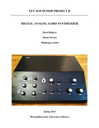
  • 1. EET 4110 SENIOR PROJECT II __________________________________________________________ DIGITAL ANALOG AUDIO SYNTHESIZER Ryan Halgren Shaun Weston Mindaugas Sanko Spring 2015 Metropolitan State University of Denver
  • 2. 1 | P a g e - S y n t h e s i z e r TABLE OF CONTENTS Executive Summary ..............................................................................................................................2-6 Introduction ...........................................................................................................................................2 Project goal ........................................................................................................................................ 2-3 Problems ................................................................................................................................................3 How it works ...................................................................................................................................... 3-4 Code .......................................................................................................................................................5 Circuits .............................................................................................................................................. 5-6 Conclusion .............................................................................................................................................6 Project Costs ............................................................................................................................................7 Project Plan .............................................................................................................................................8 Appendix ..................................................................................................................................................9 Arduino Code .................................................................................................................................. 9-12 Circuit Details and schematics ...................................................................................................... 12-18 Build and Assembly Pictures ......................................................................................................... 22-24 Resources ...............................................................................................................................................25 Data sheet links .....................................................................................................................................26 Executive Summary
  • 3. 2 | P a g e - S y n t h e s i z e r Introduction A synthesizer is an electronic musical instrument that creates musical tones by generating electronic signals. The generated waveforms can be converted into audible sound using a speaker or headphones. Synthesizers can either imitate other instruments or generate new timbres that can only be made via electronic circuitry. There are various methods to generate the signal and various methods to control the signal as well. The main components of a synthesizer and their purpose are listed below: 1. The Oscillators, which generate the tones. 2. The LFO (Low Frequency Oscillator), which usually modulates either the frequency or gain of the waveform generated by the oscillators. 3. The Filter, which emphasizes and/or removes certain frequencies. 4. The Envelope Generator, which controls changes in frequency or gain over the duration of the note. 5. The Amplifier, which controls the overall gain of the synthesizer. Today nearly all popular music involves a synthesizer and much of it uses the synthesizer as the lead instrument or as the only instruments. Most genres of music preferred by the younger generations use synthesizers as the main instrument and they have become the tool of choice for aspiring musicians. Project goal The purpose of this project was to build an affordable audio synthesizer that is composed of both digital and analog circuits. As electrical engineering students we need to be viable in both the digital and the analog curriculum. With the synthesizer, there are multiple ways in which the analog and digital aspects can be implemented. For the digital side, we used a reprogrammable microcontroller to generate the sound waveforms. Using code to design our signals allows for the type of synthesis and the signals generated by the oscillators to be changed. From the digitally generated analog output of the microcontroller, the waveform is sent through a series of analog circuits to modulate or augment the waveform. These circuits include: Low Frequency Oscillator, State Variable Filter, Envelope Generator, Ring Modulator, Voltage Controlled Amplifier and Bass Control. The signal will then be output to an audio jack so it can be played through a speakers for the user to hear. Key aspects that we aimed for in project proposal: Affordability: o We were able to stay in budget with spending under $175. We were able to accomplish building a synthesizer design that is much more affordable to own or to build yourself. Reprogrammable: o We were able to use a microcontroller to provide the oscillations. The synthesizer is be programmable, but the output pin need to be re-wired for some of the different kinds of synthesis code. This makes it more user friendly for engineers than for the average user. Customized for the user: o The microcontroller can be reprogrammed and customized with a small amount of rewiring. The analog circuits are fixed, but there is room in the enclosure for more circuits and extra connection pins soldered onto the current circuit boards so that
  • 4. 3 | P a g e - S y n t h e s i z e r additional modulation circuits can be connected in the future. Also it can take an external input signal from another synthesizer or instrument and modulate its sound with the LFO, Filters etc. Problems The most difficult tasks and our biggest problem was interfacing the keyboard with the microcontroller and ensuring that we were able to read all of the keys correctly with the number of analog read inputs on available. We did not realize when we proposed this project how difficult it was to create a piano style keyboard to control an electronic musical instrument. For now we have a potentiometer knob to turn to different positions to control the note. We wanted to use the Arduino Due for our microcontroller because It has a very high sampling rate, 512kbs of programming memory, a ton of ports and has a built in analog to digital converter so it can generate a sound with code and give an actual analog output of that function. However, we encountered issues with the Due that we did not foresee. We wanted the Due to allow frequency changes when a note was being pressed, but the Due does not allow frequency changes in the input pins and have a fixed value for each pin. This made us fall behind in building the key interface. To fix this issue, we decided to go with an external keyboard known as the Midi keyboard. We were not able to attach it for the presentation since we needed a part that has not arrived yet in order to attach a midi keyboard. This would have allowed us to have a keyboard interface, but it would be an external plug in instead of being attached with the synthesizer. How it Works The block diagram for our synthesizer design in Figure 1 below shows the parts of the synth and how the circuits interconnect. The audio signal flow is shown by the black arrows and the orange arrows represent control voltage signals. For what we were able to get working by the end of the semester we simply have a potentiometer connected to the 5 volt pin of the micro controller for our keyboard control voltage to determine the note being played. From the Microcontroller output pin the signal goes through a basic Audio Amplifier circuit with a small gain to boost the signal so that it will work correctly with the analog circuits. From there it goes to the Ring Modulator, which is how the control voltage waveform from the Low Frequency Oscillator modulates the sound. The LFO waveform is a sinusoidal signal with variable shape and speed which controls the volume of the signal through amplitude modulation. After the Ring Modulator the signal goes to the first Voltage Controlled Amplifier to allow the Envelope Generator to shape and control the gain of the signal. The Envelope Generator is triggered by a voltage pulse from the micro-controller or from a manual push button connected to the positive voltage rail. Once triggered the Envelope Generator shapes the a voltage signal to have a rise and fall to it, instead of an instantaneous change from low to high and high to low. The Voltage Controlled Amplifier allows this voltage shape to control the rise and fall of the volume of the signal for each time the E.G. is triggered.
  • 5. 4 | P a g e - S y n t h e s i z e r Figure 1. Synthesizer Flow Chart The next stage is the State Variable Filter, which allows the user to select and filter out certain frequencies through High Pass, Low Pass and Band Pass filters. The Bass Volume Control circuit is fairly simple, it just cuts or boosts the low frequencies (~300Hz and under). The final stage is another Voltage Controlled Amplifier which reads the voltage through a potentiometer to control the overall gain of the synthesizer sound. Code (see Appendix for code and details) The microcontroller can be reprogrammed with different types of oscillators but the output pins of the micro controller have to be rewired when the code is changed. We have two versions of oscillator code. One uses the Pulse Width Modulation output and can be used with most Arduino types. The second is only compatible with the Arduino Due and uses the digital to analog converter output to generate programmed waveforms. Circuits (see Appendix for circuit details and schematics) Audio Amplifier: The Audio Amplifier circuit that we decided to use is a very simple amplifier with a gain of only 5 to try to avoid noise. The design is based on the schematic given on the data sheet an IC. We changed the value of select passive components to get the gain we desired.
  • 6. 5 | P a g e - S y n t h e s i z e r Low Frequency Oscillator: The LFO signal is used as a periodic control to modulate other component’s value. Our LFO modulates the amplitude of the signal via a four quadrant multiplier (ring modulator). Our LFO design has multiple waveform outputs to select from including square, saw/triangle, pulse and parabolic. The three adjustable parameters are speed, shape and mix. The speed is variable from 1Hz to 33Hz. Ring Modulator: Allows the Low Frequency Oscillator to control the amplitude of the signal through amplitude modulation. We used a four quadrant multiplier rather than a two quadrant to eliminate the bleed through of the LFO into the audio signal. This way the LFO signal is not heard, just the effect of the LFO on the audio signal is heard. Envelope generator: The Envelope Generator is used to help shape the sound, a rise and fall in volume, of each note. The general form of an envelope filter is an ADSR (Attack, Decay, Sustain, Release). This helps control the time it takes for the note to rise to its peak volume, how long it will remain at its peak and how long it will take to return to zero volume once the note is released. Our E.G. design implements the standard ADSR form and can be triggered manually by a button for use with a continuous signal.  Attack time is the time taken for initial run-up of level from nil to peak, beginning when the key is first pressed.  Decay time is the time taken for the subsequent run down from the attack level to the designated sustain level.  Sustain level is the level during the main sequence of the sound's duration, until the key is released.  Release time is the time taken for the level to decay from the sustain level to zero after the key is released (2). Voltage Controlled Amplifier: The VCA allows a voltage (whether DC or AC signal) to control the gain of the signal being passed through the amplifier. The effect is a similar sound to the Ring Mod and uses the same transconductance amplifier input to control the signal. For our first VCA the E.G. creates the shaped voltage ‘pulse’ to change the volume each time it is triggered. Our second VCA uses a variable DC voltage to control the volume of the signal. Filters: The Type of filter that we decided to use for our synthesizer is a State Variable Filter. It is a cascaded system which simultaneously outputs a High-Pass, Low-Pass and Band-Pass response using active filters. We chose this type of design because it allows the operator to rather easily switch between filter types. The typical design uses three or more operational amplifiers with a summing amplifier and two integrators. The two resistors in the integrators must remain equal for the filters to vary the cutoff frequencies in unison while maintaining a stable phase response. This is a very flexible system because a second order response can be achieved with the HP and LP or a high gain can be achieved by the BP, depending on the Q value. The cutoff frequency and Q value-(inverse of damping coefficient) are
  • 7. 6 | P a g e - S y n t h e s i z e r adjustable via two potentiometers. In musical terms adjustable Q value of a filter is known as resonance of the filter. Bass Volume Control: The Bass Volume Control is a frequency selective circuit that give a positive or negative gain in decibels (boost or cut) at frequencies of 300Hz or less. This controls the bass range of frequencies without having any effect of the high or treble frequencies. Power Supply: We used a +15 volt DC power supply that takes the standard 120v @ 60Hz. We used some 12 volt regulators to lower the output to +12 volts. We also had to add a load to the 5 volt output of the power supply to draw current from the +15 volt outputs. Keyboard & box enclosure: (see Appendix for circuit details) The box enclosure for the synthesizer is made of oak and plywood. The wood is stained and finished for a good look and feel. The 15 volt power supply mounted securely inside the wood enclosure with the plug and switch exposed. The box has rubber feet screwed to the bottom so that it will sit securely on any surface. 5/8 inch standoff were used to support the circuit boards inside the enclosure. Conclusion In completing this project we were able to meet all of the goals we set for ourselves in our senior 1 proposal except for the keyboard interface. We were able to build a reprogrammable musical synthesizer with a digital oscillator and analog modulation circuits. We stayed under our predicted budget and built a synthesizer with customizable features that is less than half the cost of any synthesizer on the market. As electrical engineering students, it is critical for us to know analog and digital circuits and how they are inter connected. An audio synthesizer is an excellent project for students to gain experience applying their knowledge of both circuit types. This project had us programming, designing analog circuits, building circuits and soldering, building an enclosure box and interfacing with a microcontroller. The variety, difficulty and amount of work made this project a great challenge. Because this was a challenging project, we think it was one of the best learning experience of our academic career. It was incredibly fun designing this synthesizer and we will be continuing to write new versions of oscillator code and design additional circuits.
  • 8. 7 | P a g e - S y n t h e s i z e r Project Costs Parts Quantity Cost per Part Total LM13700 OTA 2 $2.00 $4.00 TL072 dual op-amp 7 $0.30 $2.10 TL074 quad op-amp 1 $0.40 $0.40 BC547 NPN transistor 5 $0.10 $0.50 7555 Timer 1 $0.45 $0.45 Capacitors (various values) 15 $0.30 $4.50 10K pot linear 2 $1.55 $3.10 100k pot Linear 3 $1.55 $4.65 50k pot linear 1 $1.55 $1.55 500k pot linear 1 $1.00 $1.00 10k pot Logarithmic 5 $0.50 $2.50 100k pot Logarithmic 2 $1.00 $2.00 1M pot Logarithmic 3 $1.00 $3.00 dual gang 10k pot Logarithmic 1 $2.50 $2.50 Resistors (various values) 52 $0.10 $5.20 1/4 inch Audio Jack 1 $2.00 $2.00 7812, 7912 (voltage Regulators) 3 $0.50 $1.50 Switches 3 $1.50 $4.50 Buttons 2 $1.50 $3.00 Ferrite Beads 2 $0.10 $0.20 4n35 Optocoupler 1 $0.50 $0.50 PCB's 2 $8.00 $16.00 +15 volt Power Supply 1 $5.00 $5.00 Arduino Due 1 $50.00 $50.00 Programming Cable 1 $10.00 $10.00 Knobs 15 $1.00 $15.00 1N4148 Diodes 8 $0.10 $0.80 Wires & Solder - $5.00 $5.00 Midi Jack 1 $4.00 $4.00 Rubber Feet 4 $0.50 $2.00 Standoffs 10 $0.20 $2.00 Wood Screws 16 $0.15 $2.40 Wood - $7.00 $7.00 Stain - $4.00 $4.00 Glue - $2.00 $2.00 TOTAL: $174.35 Figure 2. Table of part costs
  • 9. 8 | P a g e - S y n t h e s i z e r Senoir Project Plan (Above shows the original project plan, below is the actual time line) Figure 3. Project Plan vs. Project Outcome
  • 10. 9 | P a g e - S y n t h e s i z e r Appendix Synth Basics: The possible waveform synthesis techniques that our design is capable of are:  Additive synthesis  Wavetable synthesis  Sample-based synthesis  Pulse width modulation synthesis Development of the microcontroller: Figure 4. Arduino Due Microcontroller We currently have two types of code (two types of synthesis) to load onto the Arduino to create the oscillators. The first version uses C code based on the open-source code for the Auduino (audio- Arduino) project. The code we found uses grain frequency changes through Pulse Width Modulation to generate the sound and only uses 1 input pin to read pitch varied by a potentiometer. The sound is generated by the PWM output of the micro controller. We plan to build off of this code to allow a midi- controller to be read by the microcontroller to determine the note rather than a potentiometer. For the second version of the code we wanted to use the Digital to Analog convert output of the Arduino Due to produce an oscillator. This code produces four different types of oscillator waveforms: sine wave, square wave, triangle wave and saw tooth wave. The way we constructed this is by first having a mapped full cycle of each wave. Once we have it mapped out, there is nothing more than putting it into the Due’s digital to analog convertor to get the output of each wave. The full code is shown below of how each waveform is getting mapped out, getting selected, and how it is being outputted. Code: PWM Code Preview: // Analog in 0: Grain 1 pitch // Analog in 1: Grain 2 decay // Analog in 2: Grain 1 decay // Analog in 3: Grain 2 pitch // Analog in 4: Grain repetition frequency #include <avr/io.h> #include <avr/interrupt.h>
  • 11. 10 | P a g e - S y n t h e s i z e r uint16_t syncPhaseAcc; uint16_t syncPhaseInc; uint16_t grainPhaseAcc; uint16_t grainPhaseInc; uint16_t grainAmp; uint8_t grainDecay; uint16_t grain2PhaseAcc; uint16_t grain2PhaseInc; uint16_t grain2Amp; uint8_t grain2Decay; // Map Analogue channels #define SYNC_CONTROL (4) #define GRAIN_FREQ_CONTROL (0) #define GRAIN_DECAY_CONTROL (2) #define GRAIN2_FREQ_CONTROL (3) #define GRAIN2_DECAY_CONTROL (1) uint16_t mapPentatonic(uint16_t input) { //code has mapped out note scales that are not included in this code preview uint8_t value = (1023-input) / (1024/53); return (pentatonicTable[value]); } void audioOn() { #if defined(__AVR_ATmega8__) // ATmega8 has different registers TCCR2 = _BV(WGM20) | _BV(COM21) | _BV(CS20); TIMSK = _BV(TOIE2); #elif defined(__AVR_ATmega1280__) TCCR3A = _BV(COM3C1) | _BV(WGM30); TCCR3B = _BV(CS30); TIMSK3 = _BV(TOIE3); #else // Set up PWM to 31.25kHz, phase accurate TCCR2A = _BV(COM2B1) | _BV(WGM20); TCCR2B = _BV(CS20); TIMSK2 = _BV(TOIE2); #endif // Stepped pentatonic mapping: D, E, G, A, B syncPhaseInc =mapPentatonic(analogRead(SYNC_CONTROL)); grainPhaseInc = mapPhaseInc(analogRead(GRAIN_FREQ_CONTROL)) / 2; grainDecay = analogRead(GRAIN_DECAY_CONTROL) / 8; grain2PhaseInc = mapPhaseInc(analogRead(GRAIN2_FREQ_CONTROL)) / 2; grain2Decay = analogRead(GRAIN2_DECAY_CONTROL) / 4; } SIGNAL(PWM_INTERRUPT) { uint8_t value; uint16_t output; syncPhaseAcc +=syncPhaseInc; if (syncPhaseAcc < syncPhaseInc){ // Time to start the next grain grainPhaseAcc = 0; grainAmp = 0x7fff; grain2PhaseAcc = 0;
  • 12. 11 | P a g e - S y n t h e s i z e r grain2Amp = 0x7fff; LED_PORT ^= 1 << LED_BIT; // Faster than using digitalWrite } DAC code: #include "Waveforms.h" #include "Arduino.h" #define oneHzSample 1000000/maxSamplesNum // sample for the 1Hz signal expressed in microseconds const int wavebutton = 2, octane = 9, key1 = 3, key2 = 4, key3 = 5, key4 = 6, key5 = 7; volatile int wave1 = 0, octaneChange = 0; int keyfound = 0, i = 0; int sample; void setup() { analogWriteResolution(12); // set the analog output resolution to 12 bit (4096 levels) analogReadResolution(12); // set the analog input resolution to 12 bit //pinMode (key1, INPUT); //pinMode (key2, INPUT); //pinMode (key3, INPUT); //pinMode (key4, INPUT); //pinMode (key5, INPUT); attachInterrupt(wavebutton,wave1Select, RISING); // Interrupt attached to the button connected to pin 3 //attachInterrupt(octane,OctaneSelect, RISING); } void loop(){ //while(digitalRead(key1) == HIGH || digitalRead(key2) == HIGH || digitalRead(key3) == HIGH || digitalRead(key4) == HIGH || digitalRead(key5) == HIGH )//{ // Read the the potentiometer and map the value between the maximum and the minimum sample available // 1 Hz is the minimum freq for the complete wave // 170 Hz is the maximum freq for the complete wave. Measured considering the loop and the analogRead() time sample = map(analogRead(A0), 0, 4095, 0, oneHzSample); sample = constrain(sample, 0, oneHzSample); analogWrite(DAC1, waveformsTable[wave1][i]); // write the selected waveform on DAC1 i++; if(i == maxSamplesNum) // Reset the counter to repeat the wave i = 0; delayMicroseconds(sample); // Hold the sample value for the sample time //}} // function hooked to the interrupt on digital pin 3 void wave1Select() { wave1++; if(wave1 == 4) wave1 = 0;} Waveforms file: #ifndef _Waveforms_h_ #define _Waveforms_h_ #define maxWaveform 4 #define maxSamplesNum 120 static int waveformsTable[maxWaveform][maxSamplesNum] = { // Sin wave { 0x7ff, 0x86a, 0x8d5, 0x93f, 0x9a9, 0xa11, 0xa78, 0xadd, 0xb40, 0xba1,
  • 13. 12 | P a g e - S y n t h e s i z e r 0xbff, 0xc5a, 0xcb2, 0xd08, 0xd59, 0xda7, 0xdf1, 0xe36, 0xe77, 0xeb4, 0xeec, 0xf1f, 0xf4d, 0xf77, 0xf9a, 0xfb9, 0xfd2, 0xfe5, 0xff3, 0xffc, 0xfff, 0xffc, 0xff3, 0xfe5, 0xfd2, 0xfb9, 0xf9a, 0xf77, 0xf4d, 0xf1f, 0xeec, 0xeb4, 0xe77, 0xe36, 0xdf1, 0xda7, 0xd59, 0xd08, 0xcb2, 0xc5a, 0xbff, 0xba1, 0xb40, 0xadd, 0xa78, 0xa11, 0x9a9, 0x93f, 0x8d5, 0x86a, 0x7ff, 0x794, 0x729, 0x6bf, 0x655, 0x5ed, 0x586, 0x521, 0x4be, 0x45d, 0x3ff, 0x3a4, 0x34c, 0x2f6, 0x2a5, 0x257, 0x20d, 0x1c8, 0x187, 0x14a, 0x112, 0xdf, 0xb1, 0x87, 0x64, 0x45, 0x2c, 0x19, 0xb, 0x2, 0x0, 0x2, 0xb, 0x19, 0x2c, 0x45, 0x64, 0x87, 0xb1, 0xdf, 0x112, 0x14a, 0x187, 0x1c8, 0x20d, 0x257, 0x2a5, 0x2f6, 0x34c, 0x3a4, 0x3ff, 0x45d, 0x4be, 0x521, 0x586, 0x5ed, 0x655, 0x6bf, 0x729, 0x794 }, // Triangular wave { 0x44, 0x88, 0xcc, 0x110, 0x154, 0x198, 0x1dc, 0x220, 0x264, 0x2a8, 0x2ec, 0x330, 0x374, 0x3b8, 0x3fc, 0x440, 0x484, 0x4c8, 0x50c, 0x550, 0x594, 0x5d8, 0x61c, 0x660, 0x6a4, 0x6e8, 0x72c, 0x770, 0x7b4, 0x7f8, 0x83c, 0x880, 0x8c4, 0x908, 0x94c, 0x990, 0x9d4, 0xa18, 0xa5c, 0xaa0, 0xae4, 0xb28, 0xb6c, 0xbb0, 0xbf4, 0xc38, 0xc7c, 0xcc0, 0xd04, 0xd48, 0xd8c, 0xdd0, 0xe14, 0xe58, 0xe9c, 0xee0, 0xf24, 0xf68, 0xfac, 0xff0, 0xfac, 0xf68, 0xf24, 0xee0, 0xe9c, 0xe58, 0xe14, 0xdd0, 0xd8c, 0xd48, 0xd04, 0xcc0, 0xc7c, 0xc38, 0xbf4, 0xbb0, 0xb6c, 0xb28, 0xae4, 0xaa0, 0xa5c, 0xa18, 0x9d4, 0x990, 0x94c, 0x908, 0x8c4, 0x880, 0x83c, 0x7f8, 0x7b4, 0x770, 0x72c, 0x6e8, 0x6a4, 0x660, 0x61c, 0x5d8, 0x594, 0x550, 0x50c, 0x4c8, 0x484, 0x440, 0x3fc, 0x3b8, 0x374, 0x330, 0x2ec, 0x2a8, 0x264, 0x220, 0x1dc, 0x198, 0x154, 0x110, 0xcc, 0x88, 0x44, 0x0 }, // Sawtooth wave { 0x22, 0x44, 0x66, 0x88, 0xaa, 0xcc, 0xee, 0x110, 0x132, 0x154, 0x176, 0x198, 0x1ba, 0x1dc, 0x1fe, 0x220, 0x242, 0x264, 0x286, 0x2a8, 0x2ca, 0x2ec, 0x30e, 0x330, 0x352, 0x374, 0x396, 0x3b8, 0x3da, 0x3fc, 0x41e, 0x440, 0x462, 0x484, 0x4a6, 0x4c8, 0x4ea, 0x50c, 0x52e, 0x550, 0x572, 0x594, 0x5b6, 0x5d8, 0x5fa, 0x61c, 0x63e, 0x660, 0x682, 0x6a4, 0x6c6, 0x6e8, 0x70a, 0x72c, 0x74e, 0x770, 0x792, 0x7b4, 0x7d6, 0x7f8, 0x81a, 0x83c, 0x85e, 0x880, 0x8a2, 0x8c4, 0x8e6, 0x908, 0x92a, 0x94c, 0x96e, 0x990, 0x9b2, 0x9d4, 0x9f6, 0xa18, 0xa3a, 0xa5c, 0xa7e, 0xaa0, 0xac2, 0xae4, 0xb06, 0xb28, 0xb4a, 0xb6c, 0xb8e, 0xbb0, 0xbd2, 0xbf4, 0xc16, 0xc38, 0xc5a, 0xc7c, 0xc9e, 0xcc0, 0xce2, 0xd04, 0xd26, 0xd48, 0xd6a, 0xd8c, 0xdae, 0xdd0, 0xdf2, 0xe14, 0xe36, 0xe58, 0xe7a, 0xe9c, 0xebe, 0xee0, 0xf02, 0xf24, 0xf46, 0xf68, 0xf8a, 0xfac, 0xfce, 0xff0 }, // Square wave { 0xfff, 0xfff, 0xfff, 0xfff, 0xfff, 0xfff, 0xfff, 0xfff, 0xfff, 0xfff, 0xfff, 0xfff, 0xfff, 0xfff, 0xfff, 0xfff, 0xfff, 0xfff, 0xfff, 0xfff, 0xfff, 0xfff, 0xfff, 0xfff, 0xfff, 0xfff, 0xfff, 0xfff, 0xfff, 0xfff, 0xfff, 0xfff, 0xfff, 0xfff, 0xfff, 0xfff, 0xfff, 0xfff, 0xfff, 0xfff, 0xfff, 0xfff, 0xfff, 0xfff, 0xfff, 0xfff, 0xfff, 0xfff, 0xfff, 0xfff, 0xfff, 0xfff, 0xfff, 0xfff, 0xfff, 0xfff, 0xfff, 0xfff, 0xfff, 0xfff, 0x0, 0x0, 0x0, 0x0, 0x0, 0x0, 0x0, 0x0, 0x0, 0x0, 0x0, 0x0, 0x0, 0x0, 0x0, 0x0, 0x0, 0x0, 0x0, 0x0, 0x0, 0x0, 0x0, 0x0, 0x0, 0x0, 0x0, 0x0, 0x0, 0x0, 0x0, 0x0, 0x0, 0x0, 0x0, 0x0, 0x0, 0x0, 0x0, 0x0, 0x0, 0x0, 0x0, 0x0, 0x0, 0x0, 0x0, 0x0, 0x0, 0x0, 0x0, 0x0, 0x0, 0x0, 0x0, 0x0, 0x0, 0x0, 0x0, 0x0 }};#endif
  • 14. 13 | P a g e - S y n t h e s i z e r Audio Amplifier: Our Amplifier desing is based on the simple LM386 audio amplifier circuit given below. We simply adjusted the resistor values to give us a gain of 5 rather than a gain of 20. With a gain of 20 we thought we were getting to much noise and decided to lower the gain to 5. This seemed to be just enough to strengthen the signal from the microcontroller without having to much noticible noise. Figure 5. Basic LM386 Audio Amplifier Circuit LFO: Figure 6. Low Frequency Oscillator Schematic (based on Schmidt Trigger)
  • 15. 14 | P a g e - S y n t h e s i z e r Our Low Frequency Oscillator Design is based on the standard schmitt trigger and integrator oscillator core. The first potentiometers in the integrator path allows for the speed to be adjusted. The second potentiometer, after the two diodes, allows the user to adjust charge versus discharge time. Adjusting charge to discharge ratio allows the triangle/saw output to be changed from triangle, to sawtooth and reverse sawtooth waves. The discharge vs charge also has an interesting effect on the pulse output of the Schmitt trigger. As the ratio is changed, the duty cycle of the pulse is changed and becomes a variable duty cycle square wave. Because there is always half of the saw/triangle wave above 0 volts, a comparator referenced to ground is used to generate a square wave from the output of the integrator. The shape of the square wave is independent of the charge direction but the adjustment of the charge direction does change the phase of the square wave. After the comparator stage is a buffered voltage divider to reduce the square wave to a more suitable level. This also drives one side of the variable output mixer pot, while the triangle wave from the integrator drives the other side. The final op-amp is used as a buffer for the output of the variable mixer. Integrator Calculations: Fc = 1/(2*pi*R*C) = 1/(2*pi*15kohms*330nf) Fc = 33Hz LFO Variable Output Waveforms: Figure 7. LFO variable waveforms through oscilloscope
  • 16. 15 | P a g e - S y n t h e s i z e r Ring Modulator/Four Quadrant Multiplier: Figure 8. Ring Modulator Schematic Figure 8 shows how and Operational Transconductance Amplifier can be used as a ring modulator or four-quadrant multiplier. In this circuit zero carrier output is available when the modulation voltage is at zero volts, but increases when the modulation voltage moves positive or negative relative to zero. This makes it ideal for use with sinusoidal signals. The carrier output signal is inverted relative to the carrier input when the modulation voltage is positive. The carrier output is non-inverted compared to the input when the modulation voltage is negative. The Figure 8 circuit uses values suitable for operation from dual 15V supplies, but also works well with our 12V supply. The gain is determined by I-bias which is settable by adjusting the potentiometer R9 on the modulation input. How it basically works is that the OTA feeds an inverted signal current into the bottom of R7, and simultaneously the input signal feeds directly into the top of R7. R2 is set so that when the modulation input is tied to the zero volts common line, the overall gain of the OTA balances the input current of R7, and under this condition, the circuit gives zero carrier output. The adjustable R9 allows the modulation input to be changed from a value that causes almost no modulation on the output, to a value that causes excessive modulation and fold-back of the modulation signal shape on the carrier output waveform.
  • 17. 16 | P a g e - S y n t h e s i z e r Envelope generator: Figure 9. Multisim model of ADSR envelope generator circuit The core of the schematic is based on an original idea by Jonathan Jacky that was published in Electronics ("Two-chip generator shapes synthesizer's sounds" Electronics #11, September 1980 : 137- 138). Additional contributions to that design made by (Tom G.-EFM, René Schmitz). The transistor circuit that sees the gate signal before the timer is used as a buffer for the trigger signal to the timer. The first diode protects the circuit from negative voltages. The other Diodes are used to dispatch the charge and discharge current of the timing capacitor through the potentiometers. These potentiometers will control the time/level of Attack, Decay, Sustain and Release. The two op-amps are used as a simple voltage follower. How does it work ?  GATE signal is off (0V) The base of Q1 is at 0V et Q1 is blocked. The base of Q2 is at Vrail/2 and Q2 is conducting. Thus, pin 4 of the U1 is at 0V and maintains the timer in a quiet stage. Capacitor C3 is discharged and the output level is 0V.  GATE signal is on (>3V) When a gate signal occurs (>3V), Q1 comes to a conduction state, the base of Q2 comes to 0V and Q2 is blocked. Thus pin 4 of U1 is at +Vrail (15V), at the same time a brief pulse is generated by C1 at the base of Q3, the latter becomes conductive for a few hundredth of second bringing pin 2 (trigger) of U1 to 0V for a brief time. These events trigger the timer. Pin 3 (out) of U1 reaches 15V and capacitor is being charged through D3 and P1 whose value sets the Attack duration. The voltage at C3 is monitored by pin 6 (threshold) of U1. When this value reaches 2/3 of Vrail that is 10V, the timer toggles, pin 3 goes to 0Vstopping the charging of C3. Then C3 start discharging itself through D4, R12 and P2 which value sets the Decay speed, to eventually reach the voltage
  • 18. 17 | P a g e - S y n t h e s i z e r value set by the voltage divider. This divider is calculated to provide a Sustain voltage ranging from 0V to 10V. This value is held as long as the gate signal is up.  GATE signal returns to 0V (Porte/Gate : 0 V) The base of Q1 returns to 0V and Q1 is blocked. The base of Q2 is at Vrail/2 and Q2 comes to a conduction state. C4 starts discharging through D2, R13 and P3. The value of P4 sets the discharge speed that is the Release duration. Pin 4 of the 7555 is set to 0V and switches the 7555 timer to a quiet state. (2, Yusynth) Voltage controlled amplifier: Figure 10. Multisim model of voltage controlled circuit Looking at Figure 10 we see how a voltage-controlled amplifier (VCA) can be designed using a Transconductance Operational Amplifier. The input signal goes to the non-inverting terminal of the OTA through the 27k resistor which is the current limiting resistor. Then the 33k resistor determines the peak (overload) amplitude of the output while it loads the high impedance output of the OTA. The actual output signal is made available at a low-impedance level through the buffer stage through the 4.7k resistor. The voltage for the circuit in figure 10 should be powered by 9V. Here the ID current is fixed to about 0.8mA through R1 and I-bias is varied with R8 and the external gain control voltage. While the gain-control voltage is at the -9V I-bias is 0 while there is an overall ‘gain’ of -80dB within the circuit. Then with the gain-control at +9V I-bias is around 0.8mA with a voltage gain of roughly 1.5 within the circuit. This circuit is a non-inverting amplifier by using the non-inverting pin on the OTA. It could be used as an amplitude modulator or a two-quadrant multiplier through feeding the carrier signal
  • 19. 18 | P a g e - S y n t h e s i z e r to the input terminal with the modulation signal to the gain-control input terminal, much like the ring modulator circuit.. State Variable Filter: A state variable filter is basically an analog computer that continuously solves a second order differential equation. The second order response gives the HP and LP filters a roll-off slope of 40dB per decade or 12dB per octave. The first stage of the filter is the adder/subtractor, which sums the outputs from the two integrators in the later stages. The state-variable filter has many more variations than most types of filters. The signal can be applied to either the non-inverting or inverting input of the first op amp. The gain and Q value can be adjusted by changing the values of several different resistors. The corner frequencies of the HP and LP filters and the center frequency of the BP can be adjusted by raising or lowering the values of the integrator resistors. The frequencies are not altered by the gain or damping coefficient. Figure 11. State Variable Filter Block Diagram The component values of the two integrators are set equal to each other to keep the corner frequencies of the HP and LP filters equal. If these frequencies are not equal then the BP response is widened until it is very unselective or it becomes attenuated until it is nearly undetectable. Unequal corner frequencies will also cause change in the phase relationship between the LP and HP. A dual potentiometer is used to vary the two resistors in unison and maintain the BP response and phase relationship while changing the corner/center frequencies. The pass-band gain for the LP and HP filters is very close to unity. The gain of the BP filter is equal to the Q value, which is inversely proportional to the damping coefficient. The damping coefficient (α) of the state-variable filter has the same effect as it did for the single op-amp filters. For LP and HP the damping coefficient of 1.414 gives a Butterworth response, damping of 1.732 gives a Bessel response, and damping of 0.766 gives a Chebyshev response (3dB peaks). We added an extra stage to the filter to allow for independently adjustable damping and gain. We set the gain at unity and made the damping adjustable through a potentiometer. The damping coefficient is determined by the ratio between potentiometer in the negative feedback loop of the fourth op amp and the two resistors in the larger feedback loop from the second op amp (see figure 12).
  • 20. 19 | P a g e - S y n t h e s i z e r Figure 12. State Variable Filter MultiSim Schematic We chose the values of the capacitors and the dual gang potentiometer in the integrators to be able to sweep the corner frequency over the entire audible range. We decided to use a standard value of 10k ohms for the potentiometers and based on the equation Fc = 1/(2*pi*R*C), we calculated that we needed 0.33uf capacitors to give us the correct frequency range. We also put a 24 ohm stop resistor in series with the potentiometer and at 10,024 ohms the corner frequency is 48 Hz and at 24 ohms the corner frequency is 20 kHz. Filter Calculations (Note:component names in equationsrefer to Figure 4) αR = 5k + 20k pot α = damping coefficient R = 10k α = 25k/10k 5k/10k α = 2.5 0.5 Q = 1/ α Av(bp) = Q Q = 0.4 2 R1 = R2= R3= R R6= R5= Rpot R = 10k ohms C1= C2= C. Corner/Center frequency => Fc = 1/(2*pi*Rpot*C) C = 0.33uf
  • 21. 20 | P a g e - S y n t h e s i z e r Rpot = 24 ohms + 10k ohm pot Fc = 1/(2*pi*Rpot*C) Fc(min) = 1/(2*pi*10024*0.33*10^-6) Fc(min) = 48.11 Hz Fc(max) = 1/(2*pi*24*0.33*10^-6) Fc(max) = 20.095 kHz Band pass filter transfer function: High pass filter transfer function: Low pass filter transfer function:
  • 22. 21 | P a g e - S y n t h e s i z e r Figure 13. Simulation of Frequency Response of Filters It can be seen in figure 13 that the response of the HP an LP filters is of the second order and has a roll off of 40dB per decade. The BP has a first order roll off of 20dB per decade. Figure 14. Simulation of Phase Response of Filters It can be seen in figure 14 that the phase response is stable in the audible range of frequencies.
  • 23. 22 | P a g e - S y n t h e s i z e r Circuit Build: Figure 15. Circuit Board soldering pictures
  • 24. 23 | P a g e - S y n t h e s i z e r Power Supply: Figure 16. Power supply with added load on +5 volts Layout & Enclosure: Figure 17. Wood enclosure build
  • 25. 24 | P a g e - S y n t h e s i z e r Figure 18. Mounting interior components to enclosures
  • 26. 25 | P a g e - S y n t h e s i z e r Resources 1. Audiono Lo-fi synth for Arduino. http://duino4projects.com/auduino-lo-fi-synth-for-arduino/ 2. Dailey, Denton. Operational Amplifiers and Linear Integrated Circuits: Theory and Application. McGraw-Hill, 1989. 3. Envelope Generator ADSR. Yusynth. jan. 31st, 2009 http://www.yusynth.net/Modular/EN/ADSR/index_old.html. 4. Halgren, Ryan & Khokhar, Hassan. Lab 8: State-Variable Filter. EET 3120, Advanced Analog Electronics. May 6th 2014 5. http://arduino.cc/ 6. Inevitablecraftslab. Midi to Arduino. Instructables. http://www.instructables.com/id/MIDI-TO- ARDUINO/ 7. Marston, Ray. Understanding and Using ‘OTA’ Op-Amp ICs. Nuts &Volts Magazine. May, 2003. 8. Nilson, Riedel. Electric Circuits, 9th Edition. Pearson Education. 2011. 9. RCArduino. Arduino Projects, Libraries and tutorials. http://rcarduino.blogspot.com/2012/08/adding-audio-to-arduino-projects.html 10. SimpleWaveformGenerator.Arduino tutorials. http://www.arduino.cc/en/Tutorial/DueSimpleWaveformGenerator 11. Stone, Ken. Modular Synth. Modules. http://www.cgs.synth.net/ 12. Supplemental LM13700 Application Examples. http://www.idea2ic.com/LM13600/SUPPLEMENTAL%20LM13700%20APPLICATION%20E XAMPLES.html 13. Synthesizer. wikipedia. http://en.wikipedia.org/wiki/Synthesizer 14. Synth Schematics. Envelope Generator ADSR. http://www.schmitzbits.de/adsr.html 15. Texas Instruments. LM386 Low Voltage Audio Power Amplifier. August, 2000. http://www.ti.com/lit/ds/symlink/lm386.pdf .