1. SILICON PHOTOTRANSISTOR CHIPS
DEVICE NO : MC-1016
1. Application :
This specification applies to NPN silicon phototransistor chips, Device No. MC-1016
2. Structure :
2-1. Planar type .
2-2. Electrodes : N ( Emitter ) side: Aluminum alloy.
P ( Base ) side: Aluminum alloy.
N ( Collector ) side: Gold alloy.
3. Dimensions :
3-1. Chip size: 15.4 mils x 15.4 mils ( 0.390 mm x 0.390 mm ).
3-2. Chip thickness : 7.5 ± 1.0 mils ( 0.190 ± 0.025 mm ).
3-3. Active area : 11.0 mils x 11.0 mils ( 0.280 mm x 0.280 mm ).
3-4. Pattern drawing : Refer to the attached drawing.
℃
4. Electrical Characteristics (Ta= 25℃)
Parameter Symbol Condition Min. Typ. Max. Unit
Collector-Emitter
BVCEO 80 V
IC=100µA
Breakdown Voltage
Emitter-Collector
BVECO 7 V
IE=10µA
Breakdown Voltage
Collect dark Current ICEO VCE=20V 100 nA
IC=2mA
Collector-Emitter
VCE(SAT) 0.3 V
Saturation Voltage IB=100uA
IC=1mA、VCE=5V
Rise/Fall Time tR / tF 15/15 µs
RL=1000Ω
Current gain hFE 200
IC=2mA、VCE=5V
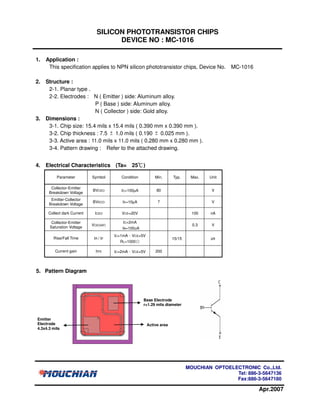
5. Pattern Diagram
Base Electrode
r=1.29 mils diameter
Emitter
Electrode Active area
4.3x4.3 mils
MOUCHIAN OPTOELECTRONIC Co.,Ltd.
Tel: 886-3-5647136
Fax:886-3-5647180
Apr.2007