Downloaded 89 times


![Design procedure
1. Calculation of maximum flux density
The core and copper losses in a transformer under Power losses in our ferrites have been measured as a
operating conditions will induce a temperature rise. function of frequency (f in Hz), peak flux density (B in
This rise must stay below a maximum allowable value to T) and temperature (T in °C). Core loss density can be
avoid damage to the transformer or the rest of the circuitry. approximated (2) by the following formula :
In thermal equilibrium the total losses in the transformer, Pcore = Cm . f x. B y. (ct0-ct1T+ct2T2) [3]
Ptrafo, can be related to a temperature rise ∆T of the peak
transformer with an analogon of Ohm’s law by:
= Cm . CT . f x. Bpeak
y [mW/cm3]
∆T
Ptrafo = [1] In this formula Cm, x ,y, ct0, ct1 and ct2 are parameters
R th
which have been found by curve fitting of the measured
In this formula Rth represents the thermal resistance of the power loss data. These parameters are specific for a ferrite
transformer. Ptrafo can in fact be interpreted as the cooling material. They are dimensioned in such a way that at
capability of the transformer. 100 °C the value of CT is equal to 1.
Previous work (1), showed that it is possible to establish In table 1 fit parameters are listed for several Ferroxcube
an empirical formula which relates the value of thermal power ferrites. Maximum allowed Pcore is calculated with
resistance of a transformer directly to the value of the equation [2]. This value is inserted in equation [3].
effective magnetic volume Ve of the ferrite core used. Maximum allowed flux density Bpeak can now be calculated
This empirical formula is valid for wire wound transformers by rewriting equation [3]:
with core shapes like RM and ETD. A similar relation has 1/y
now been found for planar E transformers. Pcore
This relation can be used to estimate the temperature rise Bpeak = [T] [4]
Cm . CT . f x
of the transformer as a function of flux density in the
core. Because of the limited available winding space it is
recommended to use the maximum allowed flux densities
in planar magnetics.
With the assumption that half of the total transformer
loss is core loss, it is possible to express the B
maximum core loss density Pcore as a function of the
allowed temperature rise ∆T of the transformer as:
2 .Bpeak
12 . ∆ T [mW/cm3]
Pcore = [2]
Ve ( cm3 )
Bpeak in the formulas is half the peak to peak flux excursion
in the core.
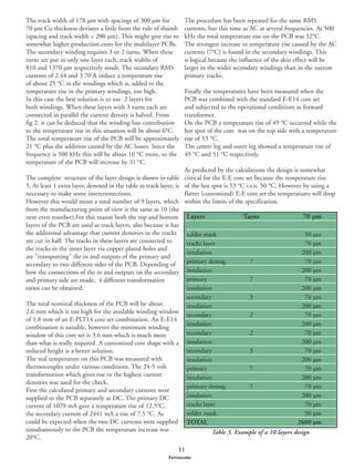
ferrite f (kHz) Cm x y ct2 ct1 ct0
3C30 20-100 7.13.10-3 1.42 3.02 3.65.10-4 6.65.10-2 4
100-200 7.13.10-3 1.42 3.02 4.10-4 6.8 .10-2 3.8
3C90 20-200 3.2.10-3 1.46 2.75 1.65.10-4 3.1.10-2 2.45
3C94 20-200 2.37.10-3 1.46 2.75 1.65.10-4 3.1.10-2 2.45
200-400 2.10-9 2.6 2.75 1.65.10-4 3.1.10-2 2.45
3F3 100-300 0.25.10-3 1.63 2.45 0.79.10-4 1.05.10-2 1.26
300-500 2.10-5 1.8 2.5 0.77.10-4 1.05.10-2 1.28
500-1000 3.6.10-9 2.4 2.25 0.67.10-4 0.81.10-2 1.14
3F4 500-1000 12.10-4 1.75 2.9 0.95.10-4 1.1.10-2 1.15
1000-3000 1.1.10-11 2.8 2.4 0.34.10-4 0.01.10-2 0.67
Table 1: Fit parameters to calculate the power loss density
4
Ferroxcube](https://image.slidesharecdn.com/planarpcbdesignguideferroxcubenopw-120307212329-phpapp01/85/Planar-pcb-design-guide-ferroxcube-no-pw-5-320.jpg)
![Note: Depending on the production capability of the PCB
The maximum allowed value for B can also be found in another way.
Formula [3] together with the fit parameters can be inserted into a
manufacturer smaller dimensions might be possible, but
computer program which makes it possible to calculate the power losses that will probably imply a substantial cost increase of the
for arbitrary wave forms (3). Advantage is that the real wave shape of B PCB.
can be simulated to calculate the losses and that it is possible to select the The number of turns per layer and the spacing between
optimum ferrite for the concerned application.
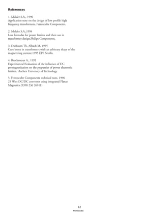
the turns are denoted by the symbols Nl and s respectively.
Then for an available winding width bw , the track width
wt can be calculated with (see fig 1):
2. Recommendations for distribution of the [ bw - (N1 + 1) . s ]
turns in the winding space wt = [5]
N1
Once the value for the maximum peak flux density In case mains insulation requirements have to be fulfilled
is determined, established formulas applicable to the the situation is somewhat different. The core is seen as a
converter topology and transformer type (e.g. flyback or part of the primary side and has to be separated 400 µm
forward) can be used to calculate the number of primary from the secondary side. Therefore, the creepage distance
and secondary turns. between the (secondary) windings close to the inner and
outer leg and the core must be 400 µm. In this case the
A decision has to be made how the windings will be track width can be calculated with [6] since 800 µm has to
divided over the available layers. Currents in the tracks will be subtracted from the available winding width.
induce a temperature rise of the PCB. It is recommended [ bw - 0.8 - (N1 - 1) . s ]
to distribute the winding turns in the outer layers wt = [6]
symmetrically with respect to the turns in the inner layers N1
for reasons of thermal expansion. In formula 5 and 6 all dimensions are in mm.
From a magnetic point of view the optimum would be
to sandwich the primary and secondary layers. This will
reduce the so called proximity effect (see page 6).
However the available winding height in the PCBs and the
required number of turns for the application will not always wt wt wt
allow an optimum design.
For cost price reasons it is recommended to choose a
standard thickness of the copper layers. Often a thickness
of 35 or 70 µm are used by PCB manufacturers. The choice
of thickness of the layers plays an important role for the
temperature rise in the windings induced by the currents. s s s s
Safety Standards like IEC 950 require a distance of 400
µm through PCB material (FR2 or FR4) for mains
insulation between primary and secondary windings. If
mains insulation is not required a distance of 200 µm
between the winding layers is sufficient. Furthermore one
has to take into account a solder mask layer of about 50 µm
on the top and bottom of the PCB. bw
The track width of a winding follows from the value of
the current and the maximum current density allowed. The
spacing between the turns is governed by the production Fig.1 Track width wt spacing s and winding width bw
capabilities and costs. A rule of thumb for a copper layer
thickness of 35 µm is a track width and spacing of
> 150 µm, and for layers of 70 µm >200 µm.
5
Ferroxcube](https://image.slidesharecdn.com/planarpcbdesignguideferroxcubenopw-120307212329-phpapp01/85/Planar-pcb-design-guide-ferroxcube-no-pw-6-320.jpg)
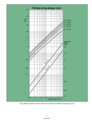
![3. Determination of temperature rise in the
PCB caused by the currents
The final step is to check the temperature rise in the The skin depth δ is the distance from the conductor surface
copper tracks induced by the currents. For this purpose towards the centre over which the current density has
the effective (= RMS) currents have to be calculated from reduced by a factor of 1/e. The skin depth depends on
the input data and desired output. The calculation method material properties as conductivity and permeability and is
depends on the topology used. In the design examples this inversely proportional to the square root of the frequency.
is shown for a conventional standard forward and flyback For copper at 60 °C the skin depth can be approximated
converter topology. An example of relations between the by: δ(µm) = 2230/(f [kHz])1/2 .
RMS currents and induced temperature rises for various When the conductor width (wt ) is taken smaller than 2δ,
cross sections of conductors in PCBs is shown in fig. 2. the contribution of this effect will be limited.This means a
For single conductor applications or inductors which are track width of <200 µm for a frequency of 500 kHz.
not too closely spaced this chart can be used directly for If there is more winding width bw available for the
determining conductor widths, conductor thickness, cross concerned number of turns, the best solution from the
sectional areas and allowed maximum currents for various magnetic point of view would be to split them up in
preset values of the temperature rise. parallel tracks.
Note: In practical situations there will be eddy current effects in
For groups of similar parallel inductors, if closely spaced, the temperature
rise may be found by using an equivalent cross section and equivalent
the conductor not only due to the alternating field of its
current. The equivalent cross section is the sum of the cross sections own current (skin effect) but also due to the fields of
of the parallel conductors and the equivalent current is the sum of the other conductors in the vicinity. This effect is called
currents in the inductor. the proximity effect. When the primary and secondary
layers are sandwiched this effect will be strongly decreased.
A shortcoming in this design approach is that the induced Reason is that the primary and secondary currents flow
heat in the windings is assumed to be caused by a DC in opposite directions so that their magnetic fields will
current while in reality there is an AC current causing skin cancel out. However there will still be a contribution to
effect and proximity effect. the proximity effect of the neighbouring conductors in the
The skin effect is the result of the magnetic field inside a same layer.
conductor generated by the conductors own current. Fast
current changes (high frequency) induce alternating fluxes Empirical tool
which cause eddy currents. These eddy currents which add Temperature measurements on several designs of multilayer
to the main current are opposite to the direction of the PCBs with AC currents supplied to the windings, show
main current. The current is cancelled out in the centre of with reasonable accuracy that up to 1MHz each increase
the conductor and moves towards the surface. The current of 100 kHz in frequency gives 2 °C extra in temperature
density decreases exponentially from the surface towards the rise of the PCB compared to the values determined for DC
centre. currents.
6
Ferroxcube](https://image.slidesharecdn.com/planarpcbdesignguideferroxcubenopw-120307212329-phpapp01/85/Planar-pcb-design-guide-ferroxcube-no-pw-7-320.jpg)
![Design example 1: Flyback transformer
minimum input voltage: Uimin = 70 V A program based on expression [3] is used to compute the
output voltage: Uo = 8.2 V losses for unipolar triangle flux wave forms with frequency
extra primary output: UpIC = 8V 120 kHz, Bpeak 160 mT and operating temperature 95 °C.
primary duty cycle: δprim ≈ 0.48/0.5 For the power ferrites 3C30, 3C90 the expected core loss
densities are 385 mW/cm3 and 430 mW/cm3.
secondary duty cycle: δsec ≈ 0.48/0.5
switching frequency f ≈120kHz Allowed core loss densities for ∆T = 35 °C are 470
output power Pmax 8W mW/cm3 for E-PLT18 and 429 mW/cm3 for E-E18
ambient temperature Tamb 60oC (from equation 1).
allowed temperature rise ∆T 35oC The conclusion is that 3C30 and 3C90 can be used in
both core combinations. Inferior ferrites with higher power
The aim is to design a flyback transformer with a losses would result in a too high temperature rise.
specification as shown above.
As a first step it is assumed that at this frequency a high The 24 primary winding turns can be divided in a
peak flux density of 160 mT can be used. Later it will symmetrical way by using 2 or 4 layers. The available
be checked whether this is possible given the allowed core winding width of the E-18 cores is 4.6 mm. This implies
losses and temperature rise. it will be a technically difficult - and therefore expensive
Table 2 shows the calculated number of turns for the six - solution to use only 2 layers with 12 turns each. This
smallest standard combinations of the Ferroxcube planar would require very narrow track widths and spacing.
E and PLT cores. Also the primary self inductance and So a choice is made for 4 layers with 6 turns each.
required airgaps and currents are calculated with formulas A lower number of layers in the multilayer PCB will result
as shown in appendix 1. in a lower cost price. Therefore we assume for the 3 turns
of the primary (for IC voltage) and for the 3 secondary
From Table 2 it can be seen that he required number of winding turns one layer each. The six layer design could be
primary turns for the E-14 core sets is too high for a built up as shown in table 3.
multilayer PCB winding. Therefore an E-E18 or E-PLT18
core combinations look the most suitable choice. Rounding
of N1, N2 and NIC results in 24, 3 and 3 respectively.
Core Ae (mm2) Ve (mm3) N1 N2 NIC G(µm) Other calculated data
E-PLT14 14.5 240 63 7.4 7.2 113 Lprim = 638 µH
E-E14 14.5 300 63 7.4 7.2 113 Ip(RMS)=186 mA
E-PLT18 39.5 800 23 2.7 2.6 41 Io(RMS)= 1593 mA
E-E18 39.5 960 23 2.7 2.6 41
E-PLT22 78.5 2040 12 1.4 1.4 22
E-E22 78.5 2550 12 1.4 1.4 22
Table 2. Calculation of data for several flyback transformers.
8
Ferroxcube](https://image.slidesharecdn.com/planarpcbdesignguideferroxcubenopw-120307212329-phpapp01/85/Planar-pcb-design-guide-ferroxcube-no-pw-9-320.jpg)
![Depending on the heat generated by the currents the Layers Turns 35 µm 70 µm
choice can be made between 35 or 70 µm copper layers.
Between primary and secondary layers a distance of 400
solder mask 50 µm 50 µm
µm is required for the mains insulation. An E-PLT 18
primary 6 35 µm 70 µm
combination has a minimum winding window of 1.8.mm.
This is sufficient for the 35 µm layer design which results in insulation 200 µm 200 µm
a PCB thickness of about 1710 µm. primary 6 35 µm 70 µm
To achieve a economic design we assumed a spacing insulation 200 µm 200 µm
of 300 µm between the tracks. Calculating the track width primary IC 3 35 µm 70 µm
for the secondary winding with [5] returns 1.06 mm, insulation 400 µm 400 µm
inclusive mains insulation. secondary 3 35 µm 70 µm
Looking in fig 2. and using the calculated (see table 2)
insulation 400 µm 400 µm
secondary RMS current of 1.6 A, results in a temperature
rise of 25 °C for the 35 µm layers and approx. 7 °C for primary 6 35 µm 70 µm
the 70 µm design. insulation 200 µm 200 µm
The temperature rise caused by the winding loss is allowed primary 6 35 µm 70 µm
to be about half the total temperature rise, in this case solder mask 50 µm 50 µm
17.5 °C. Clearly the 35 µm layers will give a too large
temperature rise for an RMS current of 1.6 A and the TOTAL 1710 µm 1920 µm
70 µm layers will have to be used.
The track widths for the primary winding turns can be Table 3. Example of a six layers design
calculated with [5] and will be approx. 416 µm. This track
width will cause hardly any temperature rise by the primary
RMS current of 0.24 A.
Because the frequency is 120 kHz, 2 °C extra temperature
rise of the PCB is expected compared to the DC current
situation. The total temperature rise of the PCB caused by
the currents only will remain below 10 °C.
This design with 6 layers of 70 µm Cu tracks should
function within its specification. The nominal thickness
of the PCB will be about 1920 µm which means that a
standard planar E-PLT18 combination cannot be used.
The standard E-E18 combination with a winding window
of 3.6 mm is usable. However its winding window is
excessive, so a customized core shape with a winding
window of approximately 2 mm would be a more elegant
solution.
Measurements on a comparable design with an E-E core
combination in 3C90 material showed a total temperature
rise of 28 °C. This is in line with a calculated contribution
of 17.5 °C temperature rise from the core losses and 10 °C
caused by winding losses.
The coupling between primary and secondary is good
because the leakage inductance turns out to be only
0.6 % of the primary inductance.
9
Ferroxcube](https://image.slidesharecdn.com/planarpcbdesignguideferroxcubenopw-120307212329-phpapp01/85/Planar-pcb-design-guide-ferroxcube-no-pw-10-320.jpg)
![Design example 2: Forward transformer
input and output voltages: 48 V 5V A final check of the core loss density at the operating
48 V 3.3 V temperature of 100 °C for the applied flux density wave
24 V 5V shapes at 530 kHz gives for 3F3 1030 mW/cm3 and for
24 V 3.3 V 3F4 1580 mW/cm3. Clearly 3F3 is the best option
The temperature rise induced in the E-PLT14 is given by:
output power: Pmax ≈ 18 W
duty cycle: δ ≈ 0.46 .
(calculated loss density 3F3/allowed loss density) ½∆T
switching frequency f ≈ 500kHz .
= ( 1030/1225 ) 25oC = 21 °C.
ambient temperature Tamb = 40oC
For the E-E14 combination this would be 23.5 °C.
allowed temperature rise ∆T = 50oC
For the primary side 7 or 14 turns are required,
depending on the input voltage. For a conventional forward
transformer the same number of turns is necessary for the
Here the aim is to design a forward transformer with
demagnetizing (recovery) winding. To make it possible to
the possibility to choose from 4 transformation ratios
use 7 or 14 primary turns and the same number of turns
which are often used in low power DC-DC converters. The
for the demagnetizing winding, 4 layers with each 7 turns
specification is shown above.
are chosen. When 7 primary and demagnetizing turns are
The first step is to check whether the smallest core
needed, the turns on 2 layers are connected in parallel. This
combinations of the standard planar E core range, the
will give the additional effect that the current density in the
E-PLT14 and E-E14, are suitable for this application.
winding tracks will be halved.
Using [2] to calculate the allowed core loss density for a
If 14 turns are necessary for the primary and demagnetizing
temperature rise of 50 °C results in 1095 mW/cm3 and
windings, the turns in two layers are connected in series so
1225 mW/cm3 for the E-E and E-PLT 14 combinations .
that the effective number of turns is 14.
With formula [3] the core loss density is calculated for
unipolar triangle flux wave forms with a frequency of 500
The available winding width for a PCB for the E 14 core is
kHz and several peak flux densities. It turns out that peak
3.65 mm. For an economic design with 300 µm spacing the
flux densities of about 100 mT will result in losses lower
track width for 7 turns per layer is 178 µm.
than the allowed core loss densities calculated with [2].
The copper layer thickness should be 70 µm because for the
The calculation of the winding turns and effective currents
24 V input the effective primary current is about 1.09 A.
is done with the formulas given in appendix 1. Using a
This gives (see fig. 2) in an effective track width of 356 µm
peak flux density of 100 mT, together with the specified
(double because of parallel connection for 7 winding turns)
data as input for the calculation, it turns out that at a
a temperature rise of 15 °C The 48 V input will result
frequency of 530 kHz the E-E14 or the E-PLT14 are usable
in an effective current of about 0.54 A. This will give in
core combinations with a reasonable number of turns .The
a track width of 178 µm (14 winding turns connected in
results of the calculations are shown in table 4.
series) a winding loss contribution to the temperature rise
of approx. 14 °C.
Core Vin Vout N1 N2 Lprim Io(RMS) Imag Ip(RMS)
(µH) (mA) (mA) (mA)
E-PLT14 48 V 5V 14 3.2 690 2441 60 543
48 V 3.3 V 14 2.1 690 3699 60 548
24 V 5V 7 3.2 172 2441 121 1087
24 V 3.3 V 7 2.1 172 3699 121 1097
E-E14 48 V 5V 14 3.2 855 2441 48 539
48 V 3.3 V 14 2.1 855 3699 48 544
24 V 5V 7 3.2 172 2441 97 1079
24 V 3.3 V 7 2.1 172 3699 97 1089
Table 4: Calculation of several forward transformers
10
Ferroxcube](https://image.slidesharecdn.com/planarpcbdesignguideferroxcubenopw-120307212329-phpapp01/85/Planar-pcb-design-guide-ferroxcube-no-pw-11-320.jpg)

This document provides a procedure for designing planar power transformers with low profiles and good thermal characteristics. The key steps are: 1) Calculate the maximum flux density based on allowed core losses and temperature rise using empirical formulas. 2) Determine the number of primary and secondary turns based on design formulas for the transformer topology (e.g. flyback, forward). 3) Distribute the winding turns across available PCB layers considering track width, spacing and insulation requirements. 4) Estimate the temperature rise in the PCB caused by AC currents using charts relating current, conductor dimensions and frequency. An example is provided for a flyback transformer design meeting given specifications. Primary turns are distributed across 2-