Ride the Storm: Navigating Through Unstable Periods / Katerina Rudko (Belka G...
SERVICE AVR 588.pdf
1. Denon Brand Company, D&M Holdings lnc.
●
For purposes of improvement, specifications and
design are subject to change without notice.
● Please use this service manual with referring to the
operating instructions without fail.
● Some illustrations using in this service manual are
slightly different from the actual set.
注 意
サービスをおこなう前に、このサービスマニュアルを
必ずお読みください。本機は、火災、感電、けがなど
に対する安全性を確保するために、さまざまな配慮を
おこなっており、また法的には「電気用品安全法」に
もとづき、所定の許可を得て製造されております。
従ってサービスをおこなう際は、これらの安全性が維
持されるよう、このサービスマニュアルに記載されて
いる注意事項を必ずお守りください。
● 本機の仕様は性能改良のため、予告なく変更すること
があります。
●
補修用性能部品の保有期間は、製造打切後 8 年です。
●
修理の際は、必ず取扱説明書を参照の上、作業を行っ
てください。
● 本文中に使用しているイラストは、説明の都合上現物
と多少異なる場合があります。
X0349 V.05 DE/CDM 0804
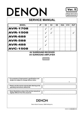
SERVICE MANUAL
AV SURROUND RECEIVER
AV SURROUND AMPLIFIER
MODEL JP E3 E2 EK E2A E1C EUT
AVR-1708 3 3
AVR-1508 3 3 3
AVR-688 3
AVR-588 3
AVR-488 3
AVC-1508 3
Ver. 5
Please refer to the
MODIFICATION NOTICE.
2. 2
AVR-1708/1508/688/588/488 AVC-1508
Please heed the points listed below during servicing and inspection.
◎ Heed the cautions!
Spots requiring particular attention when servicing, such
as the cabinet, parts, chassis, etc., have cautions indicated
on labels or seals. Be sure to heed these cautions and the
cautions indicated in the handling instructions.
◎ Caution concerning electric shock!
(1) An AC voltage is impressed on this set, so touching in-
ternal metal parts when the set is energized could
cause electric shock. Take care to avoid electric shock,
by for example using an isolating transformer and
gloves when servicing while the set is energized, un-
plugging the power cord when replacing parts, etc.
(2)There are high voltage parts inside. Handle with extra
care when the set is energized.
◎ Caution concerning disassembly and
assembly!
Though great care is taken when manufacturing parts from
sheet metal, there may in some rare cases be burrs on the
edges of parts which could cause injury if fingers are
moved across them. Use gloves to protect your hands.
◎ Only use designated parts!
The set's parts have specific safety properties (fire resis-
tance, voltage resistance, etc.). For replacement parts, be
sure to use parts which have the same properties. In par-
ticular, for the important safety parts that are marked z on
wiring diagrams and parts lists, be sure to use the desig-
nated parts.
◎ Be sure to mount parts and arrange the
wires as they were originally!
For safety reasons, some parts use tape, tubes or other in-
sulating materials, and some parts are mounted away from
the surface of printed circuit boards. Care is also taken with
the positions of the wires inside and clamps are used to
keep wires away from heating and high voltage parts, so
be sure to set everything back as it was originally.
◎ Inspect for safety after servicing!
Check that all screws, parts and wires removed or discon-
nected for servicing have been put back in their original po-
sitions, inspect that no parts around the area that has been
serviced have been negatively affected, conduct an insu-
lation check on the external metal connectors and between
the blades of the power plug, and otherwise check that
safety is ensured.
(Insulation check procedure)
Unplug the power cord from the power outlet, disconnect
the antenna, plugs, etc., and turn the power switch on. Us-
ing a 500V insulation resistance tester, check that the in-
sulation resistance between the terminals of the power
plug and the externally exposed metal parts (antenna ter-
minal, headphones terminal, microphone terminal, input
terminal, etc.) is 1MΩ or greater. If it is less, the set must
be inspected and repaired.
Concerning important safety
parts
Many of the electric and structural parts used in the set
have special safety properties. In most cases these prop-
erties are difficult to distinguish by sight, and using re-
placement parts with higher ratings (rated power and
withstand voltage) does not necessarily guarantee that
safety performance will be preserved. Parts with safety
properties are indicated as shown below on the wiring dia-
grams and parts lists is this service manual. Be sure to re-
place them with parts with the designated part number.
(1) Schematic diagrams ... Indicated by the z mark.
(2) Parts lists ... Indicated by the z mark.
Using parts other than the designated
parts could result in electric shock, fires or
other dangerous situations.
SAFETY PRECAUTIONS
The following check should be performed for the continued protection of the customer and service technician.
LEAKAGE CURRENT CHECK
Before returning the unit to the customer, make sure you make either (1) a leakage current check or (2) a line to chassis
resistance check. If the leakage current exceeds 0.5 milliamps, or if the resistance from chassis to either side of the
power cord is less than 460 kohms, the unit is defective.
CAUTION
CAUTION
9. 9
AVR-1708/1508/688/588/488 AVC-1508
CAUTION IN SERVICING
Initializing AV SURROUND RECEIVER/AM-
PLIFIER
AV SURROUND RECEIVER/AMPLIFIER initialization should
be performed when the µcom, peripheral parts of µcom, and
Digital P.W.B. are replaced.
1. Switch off the unit.
2. Hold the following SPEAKERS-A button and SPEAKERS-
B button, and switch on the unit.
3. Check that the entire display is flashing with an interval of
about 1 second, and release your fingers from the 2 but-
tons and the microprocessor will be initialized.
Note:・If step 3 does not work, start over from step 1.
・All user settings will be lost and this factory setting
will be recovered when this initialization mode.
So make sure to memorize your setting for restor-
ing after the initialization.
JIG to use for servicing
When you repair the printing board, you can use the following
JIG (Extension cable kit). Please order to Denon Official Ser-
vice Distributor in your region if necessary.
00D SPK- 561 EXTENSION UNIT KIT : 1 Set
00D SPK- 562 9120 CONN. JOINT KIT : 1 Set
When you update the firmware, you can use the following
JIG (RS232C to internal connector conversion adapter with
8P cable kit ). Please order to Denon Official Service Distrib-
utor in your region if necessary.
00DSPK-581 WRITING UNIT : 1 Set
サービス時の注意事項
AV サラウンドレシーバー / アンプの初期化
について
マイコンやマイコン周辺部品、Digital 基板等を交換した場
合は、AV サラウンドレシーバー / アンプの初期化を行って
下さい。
1. on/off ボタンを OFF にします。
2. SPEAKERS-A ボタンと SPEAKERS-B ボタンを同時に押し
ながら、on/off ボタンを押して ON にします。
3. ディスプレイ表示が約 1 秒間隔で点滅するのを確認後、
2 つのボタンから指を離します。
*マイコンが初期化されます。
注意 :・上記 3 の状態にならない場合は、もう一度操作
1 からやり直してください。
・初期化を行うとお客様が設定した内容が工場出
荷状態に戻りますので、あらかじめ設定内容を
控えておき初期化後再設定してください。
サービス時に使用する治具について
基板を修理する際、使用する治具 ( 延長ケーブルキット)
は 下記のとおりです。
必要に応じて販社サービスへ注文下さい。
00D SPK- 561 EXTENSION UNIT KIT : 1 式
00D SPK- 562 9120 CONN. JOINT KIT : 1 式
ファームウェアをアップデートする際、使用する治具
(RS232C-> 製品内部コネクタ 変換基板 +8P ケーブルキット
) は下記のとおりです。
必要に応じて販社サービスへ注文ください。
00DSPK-581 WRITING UNIT : 1 式
1,2 2,3 The illustration is AVR-1708.
s s
10. 10
AVR-1708/1508/688/588/488 AVC-1508
DISASSEMBLY
• Disassemble in order of the arrow of the figure of following flow.
下記フロー図の矢印の順番にはずしてください。
• In the case of the re-assembling, assemble it in order of the reverse of the following flow.
再組み立ての場合は、下記のフローの逆の順番に組立ててください
• In the case of the re-assembling, observe "attention of assembling" it.
再組み立ての場合は、
「組立のご注意」を遵守してください。
CABINET TOP
PANEL FRONT ASSY CHASSIS BACK ASSY TRANS
Refer to "DISASSEMBLY 1.PANEL FRONT ASSY" Refer to "DISASSEMBLY 2.CHASSIS BACK ASSY" Refer to "DISASSEMBLY 6.TRANS"
and "EXPLODED VIEW" and "EXPLODED VIEW" and "EXPLODED VIEW"
9 : POWER SW ASSY 55 : SPEAKER ASSY
10 : FUNCTION ASSY 71 : TUNER PACK
11 : FRONT ASSY
14 : HEAD PHONE ASSY CPU ASSY
21 : V. AUX ASSY Refer to "DISASSEMBLY 3.HDMI PWB ASSY"
22 : MIC ASSY and "DISASSEMBLY 4.CPU ASSY"
and "EXPLODED VIEW"
51 : CPU PWB ASSY
52 : INPUT PWB ASSY
53 : VIDEO PWB ASSY
54 : HDMI PWB ASSY
CHASSIS MAIN ASSY
Refer to "DISASSEMBLY 5.CHASSIS MAIN ASSY"
and "EXPLODED VIEW"
33 : 2CH PWB ASSY
50 : MAIN PWB ASSY
56 : POWER SUPPLY PWB ASSY
57 : POWER PWB ASSY
11. 11
AVR-1708/1508/688/588/488 AVC-1508
Picture C
Picture A
Picture D
Picture B
Picture G
( Bottom view )
The viewpoint of each photograph
(photography direction)
各図の視点(撮影方向)
[ Top view ]
Picture J
Picture I
Picture E
Picture F
Picture H
[ Top view ]
Wire clamp band
Cord holder
12. 12
AVR-1708/1508/688/588/488 AVC-1508
1. PANEL FRONT ASSY
(1) Remove the screws. ( ねじをはずす。
)
(2) Disconnect the connector wires and remove the screws . ( コネクターワイヤーとねじをはずす。
)
Proceeding ( 手順 ) : CABINET TOP → PANEL FRONT ASSY
Picture A
[ Top view ]
Picture G
[ Bottom view ]
FFC cable
Cord holder
Picture D Picture I
Cord holder
CP302 CP105
Picture C
Wire clamp band : CUT
CP503
Picture E
Wire clamp band : CUT
Cord holder
CP541
13. 13
AVR-1708/1508/688/588/488 AVC-1508
2.CHASSIS BACK ASSY
(1) Disconnect the connector wires and unscrew a screw. ( コネクタワイヤーとねじをはずす。)
Picture F
CP306
Cord holder
Please refer to "EXPLODED VIEW" for the disassembly method of each P.W.B included in panel front assy.
Panel front assy の各基板のはずしかたは "EXPLODED VIEW" を参照してください。
Proceeding ( 手順 ) : CABINET TOP → CHASSIS BACK ASSY
Picture E
CP103
CP101
CP103
CP102
FFC cable
Wire clamp band : CUT
Cord holder
Picture B Cord bush AC cord
Please refer to "EXPLODED VIEW" for the disassembly method of each P.W.B included in Chassis back assy.
Chassis back assy の各基板のはずしかたは "EXPLODED VIEW" を参照してください。
14. 14
AVR-1708/1508/688/588/488 AVC-1508
3.CPU ASSY
(1) Disconnect the connector wires and screw. ( コネクタワイヤーとねじをはずす。)
4. CHASSIS MAIN ASSY
Proceeding ( 手順 ) : CABINET TOP → CHASSIS BACK ASSY → CPU ASSY
Picture H
CP404
Connector wire
FFC cable Wire clamp band : CUT
CP904
CP406 CP405
Picture E
CP704
CP514
CP705
Please refer to "EXPLODED VIEW" for the disassembly method of each P.W.B included in CPU assy.
CPU assy の各基板のはずしかたは "EXPLODED VIEW" を参照してください。
Proceeding ( 手順 ) : CABINET TOP → CHASSIS BACK ASSY → CPU ASSY
→ CHASSIS MAIN ASSY
Please refer to "EXPLODED VIEW" for the disassembly method of each P.W.B included in chassis main assy.
Chassis main assy の各基板のはずしかたは "EXPLODED VIEW" を参照してください。
15. 15
AVR-1708/1508/688/588/488 AVC-1508
5. TRANS
(1) Disconnect the connector wires and remove the screws.(コネクタコードとねじをはずす。
)
Proceeding ( 手順 ) : CABINET TOP → TRANS
Picture E
Wire clamp band : CUT
Cord holder
CP104
CP402
CP402 CP302
CP105
Please refer to "EXPLODED VIEW" for the disassembly method of Trans.
Trans のはずしかたは "EXPLODED VIEW" を参照してください。
16. 16
AVR-1708/1508/688/588/488 AVC-1508
Check mode for µcom/DSP version s
µcom/DSP Version Display Mode
1. Operation Spec
µcom/DSP version display mode:
At its starting state, version information is displayed.
Starting method:
E3,EUT,JP model
While pressing 2 buttons, "STATUS " and "DIMMER ", turn on/off button on.
Then, press "STATUS" button to display the following information on the FL Display.
E2 model
While pressing 2 buttons, "RT " and "PTY ", turn on/off button on.
Then, press "RT" button to display the following information on the FL Display.
2. Display Order
Destination information → Main-µcom version information → DSP version information
on/off button STATUS
DIMMER
E3,EUT,JP model
on/off button RT
PTY
E2 model
18. 18
AVR-1708/1508/688/588/488 AVC-1508
ADJUSTMENT
Audio Section
Idling Current
Required measurement equipment: DC Voltmeter
1. Preparation
(1) Avoid direct blow from an air conditioner or an electric
fan, and adjust the unit at normal room temperature 15
°C ~ 30 °C (59 °F ~ 86 °F).
(2) Presetting
• POWER (Power source switch) OFF
• SPEAKER (Speaker terminal) No load
(Do not connect speaker, dummy resistor, etc.)
2. Adjustment
(1) Remove top cover and set VR101 FL, FR, C, SL, SR,
on Main Amp. Unit, VR401, VR402 on 2ch- Amp. Unit
at fully counterclockwise ( ) position.
(2) Connect DC Voltmeter to test points (FRONT-Lch:
TP101, FRONT-Rch: TP105, CENTER ch: TP103,
SURROUND-Lch: TP102, SURROUND-Rch: TP104,
SURROUND-BACK Lch: TP401, SURROUND-BACK
Rch: TP402).
(3) Connect power cord to AC Line, and turn power switch
"ON".
(4) Presetting.
MASTER VOLUME : "---" counterclockwise ( min.)
SPEAKER (Speaker terminal) : No load
(Do not connect speaker, dummy resistor, etc.)
MODE : 7CH STEREO
FUNCTION : CD
(5) Within 2 minutes after the power on, turn VR101 clock-
wise ( ) to adjust the TEST POINT voltage to
1.5 mV ± 0.5 mV DC.
(6) After 10 minutes from the preset above, turn VR101 to
set the voltage to
2.0 mV ± 0.5 mV DC.
(7) Adjust the Variable Resistors of other channels in the
same way.
VR101SR
TP104
VR101FL
TP101
TP102
VR101SL
TP402
VR402
TP103
VR101C VR101FR
TP105
F Lch S Lch
S Back Rch
TP401
VR401
S Back Lch
C ch S Rch F Rch
DC Voltmeter
MAIN AMP. UNIT
2CH AMP. UNIT
調整
オーディオセクション
アイドリング電流の調整
調整に必要な測定器 : DC Voltmeter
1. 準備
(1) セットをクーラ、扇風機のそばなど風通しの良い場
所を避け、通常の使用状態に置きます。セットの周
囲温度は 15 〜 30 ℃、湿度は常湿とします。
(2) プリセット
・電源スイッチ OFF
・スピーカ端子 無負荷
( スピーカ・ダミー抵抗器などを接続しない。)
2. 調整
(1) 上カバーをはずし、メインアンプ基板の VR101 FL,
FR, C, SL, SR 及び 2ch- アンプ基板の VR401,VR402 を
反時計方向 ( ) に回し切った状態にセットします。
(2) テストポイント (FRONT-Lch: TP101, FRONT- Rch:
TP105, CENTER ch: TP103, SURROUND-Lch: TP102,
SURROUND-Rch: TP104, SURROUND-BACK Lch:
TP401, SURROUND-BACK Rch: TP402) に DC
Voltmeter を接続します。
(3) 電源コードを AC100V(95 〜 105V の範囲でも可)
に接続し、電源スイッチを "ON" にします。
(4) ON 後、次のようにセットします。
・MASTER VOLUME(音量調節つまみ)→反時計方向
( ) に回す、最小の状態にする。
・SPEAKER(スピーカ端子)→無負荷(スピーカ、
ダミー抵抗器などを接続しない。
)
MODE : 7CH STEREO
FUNCTION : CD
(5) 2 分以内に VR101 を時計方向 ( ) に回しテストポ
イントの電圧を次のように調整します。
1.5mV ± 0.5mV DC
(6) 予備調整から 10 分後 VR101 を回し、次のように電
圧を設定します。
2.0mV ± 0.5mV DC
(7) 同じ方法で各チャネルの可変抵抗を調整します。
19. 19
AVR-1708/1508/688/588/488 AVC-1508
TROUBLE SHOOTING
1. POWER
1.1. Power not turn on
1.2. Fuse is blown
Power not turn on
Is the ON/STANDBY indicator
on the front panel flashing red?
YES
Are there any incomplete con-
nections in the connectors con-
necting between the various
circuit boards?
NO
Is there a short circuit between
the speaker terminals and the
ground?
YES
Correct the short circuit
between the speaker and the
ground.
YES NO
NO
Connect the connectors prop-
erly.
Check for damage in the power
amplifier circuitry parts and
replace any defective parts.
Is the fuse blown?
NO
Refer to Fuse is blown
YES
Does the power turn on when
the POWER switch is turned off
then back on?
NO
Is a DC 6V voltage being sup-
plied from the POWER B’d
(CN505 pins 3 and 4) to the
microprocessor?
NO
Is a DC 6V voltage output when
the cord supplying the power
from the SUPPLY B’d to the
microprocessor (CN511) is
unplugged?
NO
Check the parts from IC807 to
the primary circuitry and
replace any defective parts.
YES YES YES
Check the primary circuitry
parts including the POWER
switch (for poor contacts, etc.),
and replace any defective
parts.
Check the microprocessor
periphery circuitry and replace
any defective parts.
Check the circuitry and parts
from CN511 on the SUPPLY
B’d to the microprocessor for
damage and short-circuits, and
replace any defective parts.
Fuse is blown
Check for leaks or short circuits
in the primary side parts, and
replace any defective parts.
Check for short circuits in the
rectifier diodes and circuitry of
the secondary side rectifying
circuits, and replace any defec-
tive parts.
Check for short circuits in the
power stabilizer unit's regula-
tor output terminal and the
ground, and replace any defec-
tive parts.
After repairing, also replace the fuse.
トラブルシューティング
1. 電源
1.1. 電源が入らない
1.2. ヒューズが断線している
電源が入らない
フ ロ ン ト パ ネ ル の
ON/STANDBY インジ
ケータが赤色点滅しています
か?
YES
各基板間を接続しているコネ
クターに不完全な接続部分は
ありますか?
NO SP 端子と GND 間が短絡してい
ますか?
YES SP 端子と GND 間の短絡を取り
除いてください。
YES NO
NO コネクターを正しく接続して
ください。
POWER AMP 回路の部品の破損
を確認し、不良部品を交換して
ください。
ヒューズは断線していません
か?
NO ヒューズが断線しているを参
照してください。
YES
POWER SW を OFF にして、再
度 POWER SW を ON にすると
電源が入りますか?
NO
POWER 基板
(CN505 の 3、
4 番
ピン)からマイコンに DC6V が
供給されていますか?
NO
SUPPLY 基板からマイコンヘ電
源 を 供 給 し て い る コ ー ド
(CN511)を抜いて DC6V が出
力されていますか?
NO
IC807 〜 1 次回路までの部品を
確認し、不良部品を交換してく
ださい。
YES YES YES
POWER SW等を含む1次回路部
品 ( 接触不良等 ) を確認し、不
良部品を交換してください。
マイコン周辺回路を確認し、不
良部品を交換してください。
SUPPLY 基板の CN511 以降か
らマイコン電源までの回路お
よび部品の破損や短絡を確認
し、不良部品を交換してくだ
さい
ヒューズが断線している
1 次側の部品にリークまたは短
絡を確認し、不良部品を交換し
てください。
2 次側のそれぞれの整流回路
で、整流ダイオードおよび回路の
短絡を確認し、不良部品を交換
してください。
電源安定化部のレギュレータ
の出力端子と GND の短絡を確
認し、短絡している場合は、不
良部品を交換してくだい。
修理後、FUSE も交換してください。
20. 20
AVR-1708/1508/688/588/488 AVC-1508
2. Analog video
2.1. MONITOR OUT (CVBS) output NG
MONITOR OUT (CVBS) output NG ※ When checking operation, select
DVD for the function.
(COMPONENT1 input)
Checking the video convert ON/OFF settings
Video convert ON Video convert OFF
Input
CVBS
Input
S
Input
COMPONENT
Input
CVBS
Input
S
Input
COMPONENT
A B Progressive
no output
A No output No output
2. アナログビデオ
2.1. MONITOR OUT (CVBS) 出力 NG
MONITOR OUT (CVBS) 出力 NG ※ 動作を確認する時はファンクショ
ンを DVD に選択してください。
(COMPONENT1 入力 )
ビデオコンバート ON/OFF の設定確認
ビデオコンバート ON ビデオコンバート OFF
入力
CVBS
入力
S
入力
COMPONENT
入力
CVBS
入力
S
入力
COMPONENT
A へ B へ
プログレッシブ
出力されません
A へ 出力されません 出力されません
21. 21
AVR-1708/1508/688/588/488 AVC-1508
※ Unless specified, VIDEO UNIT part.
A
Input
CVBS
Check ± 5V.
+5V : CP514-2pin
-5V : CP514-3pin
NG To troubleshooting 1.1 Power not turn
on.
OK
Check input/output of analog SW.
Input : IC1001-12in
Output : IC1001-1pin
NG
Check analog SW settings.
IC1001-15pin : H
IC1001-11pin : L
NG
Check soldering of IC1003.
OK
OK Check soldering of IC1001.
Check input/output of AMP.
Input : IC1157-3pin
Output : IC1157-1pin
NG Check soldering of IC1157 and
surrounding parts.
OK
Check input/output of analog SW.
Input : IC1002-2pin
Output : IC1002-3pin
NG
Check analog SW settings.
IC1002-10pin : L
IC1002-9pin : L
NG
Check soldering of IC1003.
OK
OK Check soldering of IC1002.
Check input/output of AMP.
Input : IC1151-3pin
Output : IC1151-1pin
NG
Check soldering of IC1151.
OK
Check between main unit and monitor.
※ 特に記載がない場合は VIDEO 基板 の部品です。
A
入力
CVBS
± 5V の確認
+5V : CP514-2pin
-5V : CP514-3pin
NG
1.1 電源が入らないのトラブルシューティングへ
OK
アナログ SW の 入出力確認
入力 : IC1001-12pin
出力 : IC1001-1pin
NG
アナログ SW の 設定確認
IC1001-15pin : H
IC1001-11pi : L
NG
IC1003 のハンダ付け確認
OK
OK IC1001 のハンダ付け確認
AMP の 入出力確認
入力 : IC1157-3pin
出力 : IC1157-1pin
NG IC1157 及び周辺部品の
ハンダ付け確認
OK
アナログ SW の入出力確認
入力 : IC1002-2pin
出力 : IC1002-3pin
NG
アナログ SW の設定確認
IC1002-10pin : L
IC1002-9pin : L
NG
IC1003 のハンダ付け確認
OK
OK IC1002 のハンダ付け確認
AMP の入出力確認
入力 : IC1151-3pin
出力 : IC1151-1pin
NG
IC1151 のハンダ付け確認
OK
本体 - MONITOR 間の確認
22. 22
AVR-1708/1508/688/588/488 AVC-1508
※ Unless specified, VIDEO UNIT part.
B
Input
S
Check ± 5V.
+5V : CP514-2pin
-5V : CP514-3pin
NG To troubleshooting 1.1 Power not turn
on.
OK
Check input/output of analog SW.
Input Y : IC1005-12pin
Input C : IC1006-12pin
Output Y : IC1005-1pin
Output C : IC1005-1pin
NG
Check analog SW settings.
IC1005-15pin : H
IC1005-11pin : L
IC1006-15pin : H
IC1006-11pin : L
NG
Check soldering of IC1003.
OK
OK Check soldering of IC1005 and IC1006.
Check input/output of AMP.
Input Y : IC1160-5pin
Input C : IC1160-3pin
Output Y : IC1160-7pin
Output C : IC1160-1pin
NG Check soldering of IC1160 and sur-
rounding parts.
OK
Check input of video driver
Input Y : IC1016-8pin
Input C : IC1016-2pin
NG
Check soldering of IC1016.
OK
Check output of video driver.
Output : IC1016-27,32pin
NG
Check soldering of IC1016.
OK
Check input/output of analog SW.
Input : IC1002-4pin
Output : IC1002-3pin
NG
Check analog SW settings.
IC1002-10pin : H
IC1002-9pin : H
NG
Check soldering of IC1003.
OK
OK Check soldering of IC1002.
Check input/output of AMP.
Input : IC1151-3pin
Output : IC1151-1pin
NG
Check soldering of IC1151.
OK
Check between main unit and monitor.
※ 特に記載がない場合は VIDEO 基板 の部品です。
B
入力
S
± 5V の確認
+5V : CP514-2pin
-5V : CP514-3pin
NG
1.1 電源が入らないのトラブルシューティングへ
OK
アナログ SW の 入出力確認
入力 Y : IC1005-12pin
入力 C : IC1006-12pin
出力 Y : IC1005-1pin
出力 C : IC1006-1pin
NG
アナログ SW の 設定確認
IC1005-15pin : H
IC1005-11pin : L
IC1006-15pin : H
IC1006-11pin : L
NG
IC1003 のハンダ付け確認
OK
OK IC1005, IC1006 のハンダ付け確認
AMP の 入出力確認
入力 Y : IC1160-5pin
入力 C : IC1160-3pin
出力 Y : IC1160-7pin
出力 C : IC1160-1pin
NG IC1160 及び周辺部品の
ハンダ付け確認
OK
ビデオドライバの入力確認
入力 Y : IC1016-8pin
入力 C : IC1016-2pin
NG
IC1016 のハンダ付け確認
OK
ビデオドライバの出力確認
出力 : IC1016-27, 32pin
NG
IC1016 のハンダ付け確認
OK
アナログ SW の入出力確認
入力 : IC1002-4pin
出力 : IC1002-3pin
NG
アナログ SW の設定確認
IC1002-10pin : H
IC1002-9pin : H
NG
IC1003 のハンダ付け確認
OK
OK IC1002 のハンダ付け確認
AMP の入出力確認
入力 : IC1151-3pin
出力 : IC1151-1pin
NG
IC1151 のハンダ付け確認
OK
本体 - MONITOR 間の確認
23. 23
AVR-1708/1508/688/588/488 AVC-1508
2.2. VCR MONITOR OUT(CVBS) Output NG
VCR/DVR MONITOR OUT(CVBS) Output NG. ※ When checking operation, select
DVD for the function.
Input
CVBS
Input
S
Input
COMPONENT
VCR : C No output No output
2.2. VCR MONITOR OUT(CVBS) 出力 NG
VCR/DVR MONITOR OUT(CVBS) 出力 NG ※ 動作を確認する時はファンクショ
ンを DVD に選択してください。
入力
CVBS
入力
S
入力
COMPONENT
VCR : C 出力されません 出力されません
24. 24
AVR-1708/1508/688/588/488 AVC-1508
※ Unless specified, VIDEO UNIT part.
C
Input
CVBS
Check ± 5V.
+5V : CP514-2pin
-5V : CP514-3pin
NG To troubleshooting 1.1 Power not turn
on.
OK
Check input/output of analog SW.
Input : IC1001-12pin
Output : IC1001-1pin
NG
Check analog SW settings.
IC1001-9pin : H
IC1001-8pin : L
NG
Check soldering of IC1003.
OK
OK Check soldering of IC1001.
Check between main unit and monitor.
※ 特に記載がない場合は VIDEO 基板 の部品です。
C
入力
CVBS
± 5V の確認
+5V : CP514-2pin
-5V : CP514-3pin
NG
1.1 電源が入らないのトラブルシューティングへ
OK
アナログ SW の入出力確認
入力 : IC1001-12pin
出力 : IC1001-1pin
NG
アナログ SW の設定確認
IC1001-9pin : H
IC1001-8pin : L
NG
IC1003 のハンダ付け確認
OK
OK IC1001 のハンダ付け確認
本体 - MONITOR 間の確認
25. 25
AVR-1708/1508/688/588/488 AVC-1508
2.3. MONITOR OUT (S) Output NG
MONITOR OUT (S) Output NG ※ When checking operation, select
DVD for the function.
(COMPONENT1 Input)
Checking the video convert ON/OFF settings
Video convert ON Video convert OFF
Input
CVBS
Input
S
Progressive
No output
Input
CVBS
Input
S
Input
COMPONENT
D E No output E No output
2.3. MONITOR OUT (S) 出力 NG
MONITOR OUT (S) 出力 NG ※ 動作を確認する時はファンクショ
ンを DVD に選択してください。
(COMPONENT1 入力 )
ビデオコンバート ON/OFF の設定確認
ビデオコンバート ON ビデオコンバート OFF
入力
CVBS
入力
S
プログレッシブ
出力されません
入力
CVBS
入力
S
入力
COMPONENT
D へ E へ 出力されません E へ 出力されません
26. 26
AVR-1708/1508/688/588/488 AVC-1508
※ Unless specified, VIDEO UNIT part.
D
Input
CVBS
Check ± 5V.
+5V : CP514-2pin
-5V : CP514-3pin
NG To troubleshooting 1.1 Power not turn
on.
OK
Check input/output of analog SW.
Input : IC1001-12pin
Output : IC1001-1pin
NG
Check analog SW settings.
IC1001-15pin : H
IC1001-11pin : L
NG
Check soldering of IC1003.
OK
OK Check soldering of IC1001.
Check input/output of AMP.
Input : IC1157-3pin
Output : IC1157-1pin
NG Check soldering of IC1157 and
surrounding parts.
OK
Check input of video driver.
Input Y : IC1016-8pin
Input C : IC1016-2pin
NG
Check soldering of IC1018.
OK
Check output of video driver.
Output Y : IC1016-27pin
Output C : IC1016-32pin
NG
Check soldering of IC1016.
OK
Check input/output of analog SW.
Input Y : IC1007-5pin
Input C : IC1007-14pin
Output Y : IC1007-3pin
Output C : IC1007-13pin
NG
Check analog SW settings.
IC1007-10pin : H
IC1007-9pin : L
NG
Check soldering of IC1003.
OK
OK Check soldering of IC1007.
Check input/output of AMP.
Input Y: IC1163-3pin
Input C: IC1163-5pin
Output Y : IC1163-1pin
Output C : IC1163-7pin
NG
Check soldering of IC1163.
OK
Check between main unit and monitor.
※ 特に記載がない場合は VIDEO 基板 の部品です。
D
入力
CVBS
± 5V の確認
+5V : CP514-2pin
-5V : CP514-3pin
NG
1.1 電源が入らないのトラブルシューティングへ
OK
アナログ SW の 入出力確認
入力 Y : IC1001-12pin
出力 : IC1001-1pin
NG
アナログ SW の 設定確認
IC1001-15pin : H
IC1001-11pin : L
NG
IC1003 のハンダ付け確認
OK
OK IC1001 のハンダ付け確認
AMP の 入出力確認
入力 : IC1157-3pin
出力 : IC1157-1pin
NG IC1157 及び周辺部品の
ハンダ付け確認
OK
ビデオドライバの入力確認
入力 Y : IC1016-8pin
入力 C : IC1016-2pin
NG
IC1018 のハンダ付け確認
OK
ビデオドライバの出力確認
出力 Y : IC1016-27pin
出力 C : IC1016-32pin
NG
IC1016 のハンダ付け確認
OK
アナログ SW の入出力確認
入力 Y : IC1007-5pin
入力 C : IC1007-14pin
出力 Y : IC1007-3pin
出力 C : IC1007-13pin
NG
アナログ SW の設定確認
IC1007-10pin : H
IC1007-9pin : L
NG
IC1003 のハンダ付け確認
OK
OK IC1007 の ハンダ付け確認
AMP の入出力確認
入力 Y : IC1163-3pin
入力 C : IC1163-5pin
出力 Y : IC1163-1pin
出力 C : IC1163-7pin
NG
IC1163 の ハンダ付け確認
OK
本体 - MONITOR 間の確認
27. 27
AVR-1708/1508/688/588/488 AVC-1508
※ Unless specified, VIDEO UNIT part.
E
Input
S
Check ± 5V.
+5V : CP514-2pin
-5V : CP514-3pin
NG To troubleshooting 1.1 Power not turn
on.
OK
Check input/output of analog SW.
Input Y : IC1005-12pin
Input C : IC1006-12pin
Output Y : IC1005-1pin
Output C : IC1005-1pin
NG
Check analog SW settings.
IC1005-15pin : H
IC1005-11pin : L
IC1006-15pin : H
IC1006-16pin : L
NG
Check soldering of IC1003.
OK
OK Check soldering of IC1005 and IC1007.
Check input/output of AMP.
Input Y : IC1160-5pin
Input C : IC1160-3pin
Output Y : IC1160-7pin
Output C : IC1160-1pin
NG Check soldering of IC1160 and sur-
rounding parts.
OK
Check input/output of AMP.
Input Y : IC1163-3pin
Input C : IC1163-5pin
Output Y : IC1163-1pin
Output C : IC1163-7pin
NG
Check soldering of IC1163.
OK
Check between main unit and monitor.
※ 特に記載がない場合は VIDEO 基板の部品です。
E
入力
S
± 5V の確認
+5V : CP514-2pin
-5V : CP514-3pin
NG
1.1 電源が入らないのトラブルシューティングへ
OK
アナログ SW の 入出力確認
入力 Y : IC1005-12pin
入力 C : IC1006-12pin
出力 Y : IC1005-1pin
出力 C : IC1006-1pin
NG
アナログ SW の 設定確認
IC1005-15pin : H
IC1005-11pin : L
IC1006-15pin : H
IC1006-16pin : L
NG IC1003 のハンダ付け確認
もしくは DIGITAL UNIT の不具合
OK
OK IC1005,IC1007 のハンダ付け確認
AMP の 入出力確認
入力 Y : IC1160-5pin
入力 C : IC1160-3pin
出力 Y : IC1160-7pin
出力 C : IC1160-1pin
NG IC1160 及び周辺部品の
ハンダ付け確認
OK
AMP の入出力確認
入力 Y : IC1163-3pin
入力 C : IC1163-5pin
出力 Y : IC1163-1pin
出力 C : IC1163-7pin
NG
IC1163 のハンダ付け確認
OK
本体 - MONITOR 間の確認
28. 28
AVR-1708/1508/688/588/488 AVC-1508
2.4. VCR MONITOR OUT(S) Output NG
VCR/DVR MONITOR OUT(S) Output NG. ※ When checking operation, select
DVD for the function.
Input
CVBS
Input
S
Input
COMPONENT
No output VCR : F No output
2.4. VCR MONITOR OUT(S) 出力 NG
VCR/DVR MONITOR OUT(S) 出力 NG ※ 動作を確認する時はファンクショ
ンを DVD に選択してください。
入力
CVBS
入力
S
入力
COMPONENT
出力されません VCR : F 出力されません
29. 29
AVR-1708/1508/688/588/488 AVC-1508
※ Unless specified, VIDEO UNIT part.
F
Input
S
Check ± 5V.
+5V : CP514-2pin
-5V : CP514-3pin
NG To troubleshooting 1.1 Power not turn
on.
OK
Check input/output of analog SW.
Input Y : IC1005-12pin
Input C : IC1006-12pin
Output Y : IC1005-14pin
Output C : IC1006-14pin
NG
Check analog SW settings.
IC1005-9pin : H
IC1005-8pin : L
IC1006-9pin : H
IC1006-8pin : L
NG Check IC1003 soldering, or DIGITAL
UNIT flaw.
OK
OK Check soldering of IC1005 and IC1006.
Check between main unit and monitor.
※ 特に記載がない場合は VIDEO 基板 の部品です。
F
入力
S
± 5V の確認
+5V : CP514-2pin
-5V : CP514-3pin
NG
1.1 電源が入らないのトラブルシューティングへ
OK
アナログ SW の入出力確認
入力 Y : IC1005-12pin
入力 C : IC1006-12pin
出力 Y : IC1005-14pin
出力 C : IC1006-14pin
NG
アナログ SW の設定確認
IC1005-9pin : H
IC1005-8pin : L
IC1006-9pin : H
IC1006-8pin : L
NG IC1003 のハンダ付け確認
もしくは DIGITAL UNIT の不具合
OK
OK IC1005,IC1006 のハンダ付け確認
本体 - MONITOR 間の確認
30. 30
AVR-1708/1508/688/588/488 AVC-1508
2.5. COMPONENT OUT 1,2 Output NG
COMPONENT OUT 1,2 Output NG. ※ When checking operation, select
DVD for the function.
(COMPONENT1 Input)
Checking the video convert ON/OFF settings.
Video convert ON Video convert OFF
Input
CVBS
Input
S
Input
COMPONENT
Input
CVBS
Input
S
Input
COMPONENT
G H I No output No output I
2.5. COMPONENT OUT 1,2 出力 NG
COMPONENT OUT 1,2 出力 NG ※ 動作を確認する時はファンクショ
ンを DVD に選択してください。
(COMPONENT1 入力 )
ビデオコンバート ON/OFF の設定確認
ビデオコンバート ON ビデオコンバート OFF
入力
CVBS
入力
S
入力
COMPONENT
入力
CVBS
入力
S
入力
COMPONENT
G へ H へ I へ 出力されません 出力されません I へ
31. 31
AVR-1708/1508/688/588/488 AVC-1508
※ Unless specified, VIDEO UNIT part.
G
Input
CVBS
Check ± 5V and +9V.
+5V : CP514-2pin
-5V : CP514-3pin
+9V : CP514-1pin
NG To troubleshooting 1.1 Power not turn
on.
OK
Check input/output of analog SW.
Input : IC1001-12pin
Output C : IC1001-1pin
NG
Check analog SW settings.
IC1001-15pin : H
IC1001-11pin : L
NG
Check soldering of IC1003.
OK
OK Check soldering of IC1001.
Check input/output of AMP.
Input : IC1157-3pin
Output : IC1157-1pin
NG Check soldering of IC1157 and
surrounding parts.
OK
Check input of video driver
Input Y : IC1016-11in
Input Cb : IC1016-13pin
Input Cr : IC1016-15pin
NG
Check soldering of IC1019.
OK
Check output of video driver.
Output Y : IC1016-24pin
Output Cb : IC1016-21pin
Output Cr : IC1016-18pin
NG
Check soldering of IC1016.
OK
Check input/output of relay.
Input Y : IC1008-36pin
Input Cb : IC1008-38pin
Input Cr : IC1008-40pin
Output Y : IC1008-27pin
Output Cb : IC1008-24pin
Output Cr : IC1008-21pin
NG
Check soldering of IC1008.
OK
Check input/output of AMP.
Input Y : IC1164-1pin
Input Cb : IC1164-3pin
Input Cr : IC1164-5pin
Output Y : IC1164-13pin
Output Cb : IC1164-11pin
Output Cr : IC1164-9pin
NG
Check soldering of IC1164.
OK
Check between main unit and monitor.
※ 特に記載がない場合は VIDEO 基板 の部品です。
G
入力
CVBS
± 5V, +9V の確認
+5V : CP514-2pin
-5V: CP514-3pin
+9V : CP514-1pin
NG
1.1 電源が入らないのトラブルシューティングへ
OK
アナログ SW の 入出力確認
入力 : IC1001-12pin
出力 C : IC1001-1pin
NG
アナログ SW の 設定確認
IC1001-15pin : H
IC1001-11pin : L
NG
IC1003 のハンダ付け確認
OK
OK IC1001 ハンダ付け確認
AMP の 入出力確認
入力 : IC1157-3pin
出力 : IC1157-1pin
NG IC1157 及び周辺部品の
ハンダ付け確認
OK
ビデオドライバの入力確認
入力 Y : IC1016-11in
入力 Cb : IC1016-13pin
入力 Cr : IC1016-15pin
NG
IC1019 のハンダ付け確認
OK
ビデオドライバの出力確認
出力 Y : IC1016-24pin
出力 Cb : IC1016-21pin
出力 Cr : IC1016-18pin
NG
IC1016 のハンダ付け確認
OK
リレー入出力の確認
入力 Y : IC1008-36pin
入力 Cb : IC1008-38pin
入力 Cr : IC1008-40pin
出力 Y : IC1008-27pin
出力 Cb : IC1008-24pin
出力 Cr : IC1008-21pin
NG
IC1008 のハンダ付け確認
OK
AMP の入出力確認
入力 Y : IC1164-1pin
入力 Cb : IC1164-3pin
入力 Cr : IC1164-5pin
出力 Y : IC1164-13pin
出力 Cb : IC1164-11pin
出力 Cr : IC1164-9pin
NG
IC1164 のハンダ付け確認
OK
本体 - MONITOR 間の確認
32. 32
AVR-1708/1508/688/588/488 AVC-1508
※ Unless specified, VIDEO UNIT part.
H
Input
S
Check ± 5V and +9V.
+5V : CP514-2pin
-5V : CP514-3pin
+9V : CP514-1pin
NG To troubleshooting 1.1 Power not turn
on.
OK
Check input/output of analog SW.
Input Y : IC1005-12pin
Input C : IC1006-12pin
Output Y : IC1005-1pin
Output C : IC1006-1pin
NG
Check analog SW settings.
IC1005-15pin : H
IC1005-11pin : L
IC1006-15pin : H
IC1006-11pin : L
NG
Check soldering of IC1003.
OK
OK Check soldering of IC1005 and IC1006.
Check input/output of AMP.
Input Y : IC1160-5pin
Input C : IC1160-3pin
Output Y : IC1160-7pin
Output C : IC1160-1pin
NG Check soldering of IC1160 and sur-
rounding parts.
OK
Check input of video driver
Input Y : IC1016-11in
Input Cb : IC1016-13pin
Input Cr : IC1016-15pin
NG
Check soldering of IC1019.
OK
Check output of video driver.
Output Y : IC1016-24pin
Output Cb : IC1016-21pin
Output Cr : IC1016-18pin
NG
Check soldering of IC1016.
OK
Check input/output of relay.
Input Y : IC1008-36pin
Input Cb : IC1008-38pin
Input Cr : IC1008-40pin
Output Y : IC1008-27pin
Output Cb : IC1008-24pin
Output Cr : IC1008-21pin
NG
Check soldering of IC1008.
OK
Check input/output of AMP.
Input Y : IC1164-1pin
Input Cb : IC1164-3pin
Input Cr : IC1164-5pin
Output Y : IC1164-13pin
Output Cb : IC1164-11pin
Output Cr : IC1164-9pin
NG
Check soldering of IC1164.
OK
Check between main unit and monitor.
※ 特に記載がない場合は VIDEO 基板 の部品です。
H
入力
S
± 5V,+9V の確認
+5V : CP514-2pin
-5V : CP514-3pin
+9V : CP514-1pin
NG
1.1 電源が入らないのトラブルシューティングへ
OK
アナログ SW の 入出力確認
入力 Y : IC1005-12pin
入力 C : IC1006-12pin
出力 Y : IC1005-1pin
出力 C : IC1006-1pin
NG
アナログ SW の 設定確認
IC1005-15pin : H
IC1005-11pin : L
IC1006-15pin : H
IC1006-11pin : L
NG
IC1003 のハンダ付け確認
OK
OK IC1005,IC1006 のハンダ付け確認
AMP の 入出力確認
入力 Y : IC1160-5pin
入力 C : IC1160-3pin
出力 Y : IC1160-7pin
出力 C : IC1160-1pin
NG IC1160 及び周辺部品の
ハンダ付け確認
OK
ビデオドライバの入力確認
入力 Y : IC1016-11in
入力 Cb : IC1016-13pin
入力 Cr : IC1016-15pin
NG
IC1019 のハンダ付け確認
OK
ビデオドライバの出力確認
出力 Y : IC1016-24pin
出力 Cb : IC1016-21pin
出力 Cr : IC1016-18pin
NG
IC1016 のハンダ付け確認
OK
リレー入出力の確認
入力 Y : IC1008-36pin
入力 Cb : IC1008-38pin
入力 Cr : IC1008-40pin
出力 Y : IC1008-27pin
出力 Cb : IC1008-24pin
出力 Cr : IC1008-21pin
NG
IC1008 のハンダ付け確認
OK
AMP の入出力確認
入力 Y : IC1164-1pin
入力 Cb : IC1164-3pin
入力 Cr : IC1164-5pin
出力 Y : IC1164-13pin
出力 Cb : IC1164-11pin
出力 Cr : IC1164-9pin
NG
IC1164 のハンダ付け確認
OK
本体 - MONITOR 間の確認
33. 33
AVR-1708/1508/688/588/488 AVC-1508
※ Unless specified, VIDEO UNIT part.
I
Input
COMPONENT
Check ± 5V and +9V.
+5V : CP514-2pin
-5V : CP514-3pin
+9V : CP514-1pin
NG To troubleshooting 1.1 Power not turn
on.
OK
Check input/output of COMPONENT.
selector
Input Y : IC1008-42pin
Input Cb : IC1008-44pin
Input Cr : IC1008-46pin
Output Y : IC1008-27pin
Output Cb : IC1008-24pin
Output Cr : IC1008-21pin
NG Check IC1008 soldering, or DIGITAL
UNIT flaw.
OK
Check input/output of AMP.
Input Y : IC1164-1pin
Input Cb : IC1164-3pin
Input Cr : IC1164-5pin
Output Y : IC1164-13pin
Output Cb : IC1164-11pin
Output Cr : IC1164-9pin
NG
Check soldering of IC1164.
OK
Check between main unit and monitor.
※ 特に記載がない場合は VIDEO 基板の部品です。
I
入力
COMPONENT
± 5V,+9V の確認
+5V : CP514-2pin
-5V : CP514-3pin
+9V : CP514-1pin
NG
1.1 電源が入らないのトラブルシューティングへ
OK
COMPONENT セレクタの入出力確認
入力 Y : IC1008-42pin
入力 Cb : IC1008-44pin
入力 Cr : IC1008-46pin
出力 Y : IC1008-27pin
出力 Cb : IC1008-24pin
出力 Cr : IC1008-21pin
NG IC1008 のハンダ付け確認
もしくは、DIGITAL UNIT の不具合
OK
AMP の入出力確認
入力 Y : IC1164-1pin
入力 Cb : IC1164-3pin
入力 Cr : IC1164-5pin
出力 Y : IC1164-13pin
出力 Cb : IC1164-11pin
出力 Cr : IC1164-9pin
NG
IC1164 のハンダ付け確認
OK
本体 - MONITOR 間の確認
34. 34
AVR-1708/1508/688/588/488 AVC-1508
2.6. HDMI OUT 1,2 Output NG
HDMI OUT 1,2 Output NG. ※ When checking operation, select
DVD for the function.
(COMPONENT1 Input)
Input
CVBS
Input
S
Input
COMPONENT
入力
HDMI
No output
To troubleshooting 3.HDMI/DVI.
2.6. HDMI OUT 1,2 出力 NG
HDMI OUT 1,2 出力 NG ※ 動作を確認する時はファンクショ
ンを DVD に選択してください。
(COMPONENT1 入力 )
入力
CVBS
入力
S
入力
COMPONENT
入力
HDMI
出力されません
3. HDMI/DVI のトラブルシューティングへ
35. 35
AVR-1708/1508/688/588/488 AVC-1508
3. HDMI/DVI
3.1. No picture or sound is output
No picture or sound is output
YES
Check the HDMI/DVI cable connection
YES
Is the HDMI/DVI cable properly
connected?
NO There may be a problem with the HDMI/
DVI cable. Check the connection.
YES
Are you using an HDMI/DVI selector,
repeater or a device for improving picture
quality?
YES Disconnect everything and connect only
the HDMI/DVI cable to check.
NO
Are you using a certified HDMI cable (one
with the HDMI stamp)?
NO Use a certified HDMI cable (one with the
HDMI stamp).
YES
Are you using an HDMI/DVI cable less
than 5 meters in length?
NO
Replace the HDMI/DVI cable with one
that is less than 5 meters in length (2
meters recommended) to check.
YES
Are the picture and sound output when
another HDMI/DVI cable is used?
YES
The HDMI/DVI cable is defective.
NO
Checking the DVD player
YES
Is the DVD player's HDMI output setting
correct?
YES
Check the HDMI output setting, referring
to the DVD player's operating
instructions.
YES
When using a DENON DVD player, is the fluorescent display tube's
"HDMI" indicator lit?
If using a non-DENON DVD player, proceed to "YES".
YES
NO
Are the picture and sound output when
the DVD player's resolution is changed?
YES
Set the DVD player's output resolution
to a resolution with which the TV is
compatible.
NO
Is sound output from the set's speaker terminals when the TV's power is
turned off or the connection cable between the TV and the set is
disconnected?
YES
The DVD player may not be compatible
with HDCP repeaters. Ask the DVD
player's manufacturer.
NO
Are the picture and sound output when a
different DVD player is used?
YES
The DVD player is defective.
NO
3. HDMI/DVI
3.1. 映像と音声が出力されない
映像と音声が出力されない
YES
HDMI/DVIケーブルの接続を確認する
YES
HDMI/DVI ケーブルは正しく接続され
ていますか?
NO
HDMI/DVI ケーブルは勘合がよくない
ことがあります。
接続を確認してくだ
さい。
YES
HDMI/DVI セレクター、リピーターや
画質改善装置を使用していますか?
YES すべて取り外してHDMI/DVIケーブル
のみを接続して確認してください。
NO
HDMI 認証品(HDMI 刻印がある)の
HDMI ケーブルを使用していますか?
NO HDMI ケーブルは HDMI 認証品
(HDMI
刻印がある)を使用してください。
YES
HDMI/DVI ケーブルは 5m 以下のもの
を使用していますか?
NO
HDMI/DVI ケーブルを 5m 以下 ( 推奨
は2 m) に交換して確認してくださ
い。
YES
別のHDMI/DVIケーブルに交換すると
画像と音声が出力されますか?
YES
HDMI/DVI ケーブルが不良です。
NO
DVD プレーヤーを確認する
YES
DVD プレーヤーの HDMI 出力設定は
正しいですか?
NO
DVD プレーヤーの取扱説明書を見て
HDMI 出力を正しく設定してくださ
い。
YES
DENON の DVD プレーヤーを使用している場合、FL 管の "HDMI" インジ
ケータが点灯していますか?
他社の DVD プレーヤーを使用している場合は "YES" に進んでください。
YES
NO DVD プレーヤーの解像度を変えて画
像と音声が出力されますか?
YES
DVD プレーヤーの出力解像度を、TV
の対応可能な解像度に設定してくだ
さい。
NO
TV の電源を切った時や TV と本機間の接続ケーブルをはずした時に、本機
のスピーカー端子から音声を出力しますか?
YES
DVD プレーヤーが HDCP リピーター
に対応していない可能性があります。
DVD プレーヤーのメーカーに確認し
てください。
NO
別の DVD プレーヤーに交換すると画
像と音声が出力されますか?
YES
DVD プレーヤーが不良です。
NO
36. 36
AVR-1708/1508/688/588/488 AVC-1508
Check the TV
Is the TV HDCP-compatible?
NO Use an HDCP-compatible TV. PC TVs
cannot be used.
YES
Is the TV compatible with resolutions of 1080P?
NO
If the TV is not compatible with
resolutions of 1080P, no picture will be
output, even if the DVD player's
resolution is set to 1080P.
YES
Is the TV's input set to HDMI?
NO Check the TV's input setting, referring to
the TV's operating instructions.
YES
Are the picture and sound output when a different TV is used?
NO
The TV is defective.
YES
Check the set (AVR-4308CI)
Is the set's input set to HDMI?
NO Check the set's input setting, referring to
the set's operating instructions.
YES YES
Is the TV information
properly displayed on
the "Monitor info."
display menu?
NO
The set does not recognize the TV.
Is IC01 pin 76 "H" (3V-5V)? With the TV
connected, check the voltage of the IC on
the side on which the TV is connected.
NO
The pattern and circuit from the HDMI
connector (JACK03) to the IC (IC01)
is defective.
YES YES
Does the set's wallpaper image appear on the TV when the HDMI/DVI
cable between the DVD player and the set is disconnected?
NO
Are the picture and sound output from
other Monitor Out terminals (VIDEO out,
S-VIDEO out or Component out)?
YES
The HDMI output
circuitry is defective.
(IC01 and surrounding
circuitry)
YES YES
NO
When using a
DENON DVD player,
is the fluorescent
display tube's "HDMI"
indicator lit?
If using a non-
DENON DVD player,
proceed to "NO".
NO
The DVD player does not recognize the
connection with the set.
Is the HDMI connector (JACK01/JACK02/
JACK03) pin 19 "H" (5V)? With the DVD
player connected, check the voltage of
the HDMI connector for the input on the
side on which the DVD player is
connected.
NO
The pattern and circuit from the HDMI
connector (JACK01/JACK02/
JACK03) to the IC12 is defective.
YES YES
The HDMI output circuitry is defective.
(IC01 and surrounding circuitry)
TV を確認する
TV は HDCP に対応していますか?
NO
HDCP に対応している TV を使用して
ください。
PC 用の TV は使用できませ
ん。
YES
TV は 1080P に対応していますか?
NO
TV が 1080P に対応していない場合、
DVD プレーヤーを 1080P に設定して
も、画像は出力されません。
YES
TV の入力設定が HDMI 入力になっていますか?
NO TV の取扱説明書を見て入力設定を確
認してください。
YES
別の TV に交換すると画像と音声が出力されますか?
NO
TV が不良です。
YES
本機を確認する
本機の入力設定が HDMI 入力になっていますか?
NO 本機の取扱説明書を見て入力設定を
確認してください。
YES
Monitor info. 表示メニュー
で TV の情報が正しく表示さ
れていますか?
NO
本機が TV を認識していません
IC01 の 76pin が "H"(3V-5V) となって
いますか?
TV を接続している状態で、TV を接続
している側の IC の電圧を確認してく
ださい。
NO
HDMI コネクター (JACK03) から
IC(IC01)までのパターンおよび回路が
不良です。
YES YES
DVD プレーヤーと本機間の HDMI/DVI ケーブルを取り外した時、TV に本
機の壁紙の画像が表示されますか?
NO
他の Monitor Out(VIDEO out/S-VIDEO
out/Component out) からは出力され
ますか?
YES
HDMI出力系の回路が
不良です。
(IC01 周辺回路 )
YES
NO
DENON の DVD プレーヤー
を使用している場合、FL 管
の"HDMI"インジケータが点
灯していますか?
他社の DVD プレーヤーを使
用している場合は "NO"に進
んでください。
NO
DVD プレーヤーが本機との接続を認
識していません
HDMI コネクター (JACK01/JACK02/
JACK03) の 19pin が "H"(5V) となって
いますか?
DVD プレーヤーを接続している状態
で、DVD プレーヤーを接続している
入力の HDMI コネクターの電圧を確
認してください。
NO
HDMI コネクター (JACK01/JACK02/
JACK03) から IC12 までのパターンお
よび回路が不良です。
YES YES
HDMI 入力系の回路が不良です。
(IC01 周辺回路 )
40. 40
AVR-1708/1508/688/588/488 AVC-1508
GND DIAGRAM
RDS
CPU
CN505
CP514
CN511
CP511
SP
RELAY
GND
SBL
GND
SL
GND
FRONT
L
GND
SR
GND
C
GND
PRE
SBL
GND
PRE
C
GND
CP702
CN506
CN706
HDMI
SWITCHER
SIL9185
HDMI_GND
MIC_A
GND
KEY
CPU GND
FRONT B'D
MAIN B`D
BU4094 BU4094
HP RELAY GND
CP201
CN201
ZONE2
INPUT B`D
R2A15215FP
8CH.EXT
MIC B`D
PRE_AMP
V.AUX B`D
V GND
A/D IN
V GND
CP904
CODEC
DSP
XM RADIO
CP405
CP301B
CP505
CPU GND
H/P B`D
HP GND
CP305
CP304
CN541
CN305
CN304
2CH AMP B`D
CP541
PRE
SBR
GND
FR
GND
SBR
GND
SR
GND
PRE OUT
C
GND
FRONT
R
GND
MUTE GND
CPU GND
PRE
FR
GND
CN514
SL
GND
PRE
SR
GND
CP704
CN704
V GND
CPU GND
VIDEO B`D
FL
GND
CP105
(MAIN)
CN702
(INPUT)
CN703
(INPUT)
CP703
DSP
CPU GND
8CH-LPF
IPOD
CP301A
HDMI B`D
CP804
CN804
CP802
CN802
CP803
CN803
CN904
CPU GND
D GND
DIR
HDMI
CN405
XM RADIO
XM_DAC
CP506
SBR
GND
SBR
GND
CP514
CPU
GND
V
GND
CP1002
CN1002
(VIDEO)
CN701
(INPUT)
CP701
CN805
CP805
CP01
CN01
XM_TRANCEIVER
CPU
GND
XM_GND
V
GND
V.AUX_A
GND
PRE
SL
GND
PRE
FL
GND
FUNCTION B'D
V GND
REMOTE
V GND
A GND
ZONE_A GND
XM_A GND
TUNER PACK
TUNER PACK
TUNER INPUT
ANALOG INPUT
V GND
MIC_A GND
V.AUX_A GND
MIC_A GND
PRE_RETURN_GND
HDMI INPUT
CP404
XM INPUT
POWER S/W B`D
SUPPLY B`D
POWER B`D
CPU GND
SPEAKER OUT B`D
CPU GND
S1 COMON
CURRENT LIMIT
V.AUX_A GND
TUNER_A GND
A GND
CPU GND
V.AUX_A GND
MIC_A GND
CPU B`D
CN105
BUFF AMP
CPU GND
OPTICAL
COAXIAL
CN404
PRE_RETURN_GND
SPEAKER RELAY GND
PRE_RETURN_GND
VIDEO INPUT
(S/C/COMPO VIDEO)
45. 45
AVR-1708/1508/688/588/488 AVC-1508
SEMICONDUCTORS
Only major semiconductors are shown, general semiconductors etc. are omitted to list.
主な半導体を記載しています。汎用の半導体は記載を省略しています。
1. IC’s
M30626FHPFP (IC804)
M30626FHPFP Terminal Function
PIN NO. PIN NAME I/O FUNCTION
1 P96/SOUT4 SW_SUM O Bass Management Control
2 P95/CLK4 iPod DET I iPod Dock Det
3 P94/TB4 2090_CLK/SEL2 O AVR-1708 : EXPANDER Control Pin / AVR-1508 : VIDEO Control Pin
4 P93/TB3 2090_DATA/SEL1 O AVR-1708 : EXPANDER Control Pin / AVR-1508 : VIDEO Control Pin
5 P92/SOUT3 SHARC_SDOUT O DSP(IC801 : ADSP-21367)Control Pin
6 P91/SIN3 SHARC_SDIN I DSP(IC801 : ADSP-21367)Control Pin
7 P90/CLK3 SHARC _SCLK O DSP(IC801 : ADSP-21367)Control Pin
8 BYTE BYTE - GND
9 CNVCS CNVSS I UPGRADE PIN
10 P87 1328 CE O CODEC(IC808 : ADAU1328) Control Pin
11 P86 XM DACMS O XM DAC(IC06 : AK4385)Control Pin
12 RESET RESET I RESET (Det = "L")
13 XOUT X2 O Clock(12MHz )
1 2 3 4 5 6 7 8 9 10 11 12 13 14 15 16 17 18 19 20 21 22 23 24 25 26 27 28 29 30
31
32
33
34
35
36
37
38
39
40
41
42
43
44
45
46
47
48
49
50
51
52
53
54
55
56
57
58
59
60
61
62
63
64
65
66
67
68
69
70
71
72
73
74
75
76
77
78
79
80
81
82
83
84
85
86
87
88
89
90
91
92
93
94
95
96
97
98
99
100
P0_0/AN0_0/D0
P0_1/AN0_1/D1
P0_2/AN0_2/D2
P0_3/AN0_3/D3
P0_4/AN0_4/D4
P0_5/AN0_5/D5
P0_6/AN0_6/D6
P0_7/AN0_7/D7
P1_0/D8
P1_1/D9
P1_2/D10
P1_3/D11
P1_4/D12
VREF
AVSS
VCC1
XIN
XOUT
VSS
RESET
CNVSS
P8_7/XCIN
P8_6/XCOUT
BYTE
P2_0/AN2_0/A0(/D0/-)
P2_1/AN2_1/A1(/D1/D0)
P2_2/AN2_2/A2(/D2/D1)
P2_3/AN2_3/A3(/D3/D2)
P2_4/AN2_4/A4(/D4/D3)
P2_5/AN2_5/A5(/D5/D4)
P2_6/AN2_6/A6(/D6/D5)
P2_7/AN2_7/A7(/D7/D6)
P3_0/A8(/-/D7)
P3_1/A9
P3_2/A10
P3_3/A11
P3_4/A12
P3_5/A13
P3_6/A14
P3_7/A15
P4_0/A16
P4_1/A17
P4_2/A18
P4_3/A19
P7_4/TA2OUT/W
P7_6/TA3OUT
P5_6/ALE
P7_7/TA3IN
P5_5/HOLD
P5_4/HLDA
P5_3/BCLK
P5_2/RD
VCC2
VSS
P5_7/RDY/CLKOUT
P4_5/CS1
P4_6/CS2
P4_7/CS3
AVCC
P6_3/TXD0/SDA0
P6_5/CLK1
P6_6/RXD1/SCL1
P6_7/TXD1/SDA1
P6_1/CLK0
P6_2/RXD0/SCL0
P10_0/AN0
P10_1/AN1
P10_2/AN2
P10_3/AN3
P9_3/DA0/TB3IN
P9_4/DA1/TB4IN
P9_5/ANEX0/CLK4
P9_6/ANEX1/SOUT4
P9_1/TB1IN/SIN3
P9_2/TB2IN/SOUT3
P8_0/TA4OUT/U P6_0/CTS0/RTS0
P6_4/CTS1/RTS1/CTS0/CLKS1
P7_2/CLK2/TA1OUT/V
P8_2/INT0
P7_1/RXD2/SCL2/TA0IN/TB5IN
(1)
P8_3/INT1
P8_5/NMI
P9_7/ADTRG/SIN4
P4_4/CS0
P5_0/WRL/WR
P5_1/WRH/BHE
P9_0/TB0IN/CLK3
P7_0/TXD2/SDA2/TA0OUT
(1)
P8_4/INT2/ZP
P8_1/TA4IN/U
P7_3/CTS2/RTS2/TA1IN/V
P7_5/TA2IN/W
P1_5/D13/INT3
P1_6/D14/INT4
P1_7/D15/INT5
P10_7/AN7/KI3
P10_6/AN6/KI2
P10_5/AN5/KI1
P10_4/AN4/KI0
M30626FHPFP
NOTES:
1. P7_0 and P7_1 are N channel open-drain output pins.
46. 46
AVR-1708/1508/688/588/488 AVC-1508
14 VSS VSS - GND
15 XIN X1 I Clock(12MHz)
16 VCC VCC - +5V
17 P85/NMI NMI I -
18 P84/INT2 FLAG0 I DSP(IC801 : ADSP-21367) Control Pin
19 P83/INT1 POWER DOWN I Power Down Detection Pin (Det = "L")
20 P82/INT0 PROTECTION I Protect Detection (Det = "L")
21 P81 XM DAC_CLK(MC) O XM DAC(IC06 : AK4385)Control Pin
22 P80 XM DAC_DATA(MDI) O XM DAC(IC06 : AK4385)Control Pin
23 P77 FLD_RESET O FL DRIVER Control Pin
24 P76 FLD_CE O FL DRIVER Control Pin
25 P75 FLD_CLK O FL DRIVER Control Pin
26 P74 FLD_DATA O FL DRIVER Control Pin
27 P73/CTS2 2090-C_CLK O IC301 : BU2090(EXPANDER)Control Pin
28 P72/CLK2 2090-C_DATA O IC301 : BU2090(EXPANDER)Control Pin
29 P71/RXD2 RXD MIXMO I XM Radio Control Pin
30 P70/TXD2 TXD MOXMI O XM Radio Control Pin
31 P67/TXD1 TXD MO232I O Flash Starter/DENON Writer Control Pin
32 P66/RXD1 RXD MI232O I Flash Starter/DENON Writer Control Pin
33 P65/CLK1 LIMIT DET I Current Limit Detection
34 P64/CTS1 LIMIT O Current Limit Control Pin
35 P63/TXD0 TXD_iPod O iPod Dock Control Pin
36 P62/RXD0 RXD_iPod I iPod Dock Control Pin
37 P61/CLK0 XM ANT REV I XM Radio Control Pin
38 P60/CTS0 XM LINK ACTIVE I XM Radio Control Pin
39 P57 TUNED I FM/AM TUNED Detection(Det = "L")
40 P56 STEREO I FM STEREO Detection(Det = "L")
41 P55/EPM FLASH EPM I UPGRADE PIN
42 P54 VOL UP I MASTER VOLUME KNOB(Rotary Encoder) Rotational Detection
43 P53 VOL DOWN I MASTER VOLUME KNOB(Rotary Encoder) Rotational Detection
44 P52 SEL UP I SELECTOR KNOB(Rotary Encoder) Rotational Detection
45 P51 SEL DOWN I SELECTOR KNOB(Rotary Encoder) Rotational Detection
46 P50/CE FLASH CE I UPGRADE PIN
47 P47 PLL/RDS DIN O TUNER PLL(LC72131)/RDS(LC72720)Control Pin
48 P46 PLL/RDS CLK O TUNER PLL(LC72131)/RDS(LC72720) Control Pin
49 P45 PLL STB O TUNER PLL(LC72131)Control Pin
50 P44 PLL_DOUT I TUNER PLL(LC72131)Control Pin
51 P43 RDS RESET O RDS(IC805 : LC72720)Control Pin
52 P42 RDS CE O RDS(IC805 : LC72720)Control Pin
53 P41 RDS DOUT I RDS(IC805 : LC72720)Control Pin
54 P40 89057 INT I DIR(IC807 : LC89057) Control Pin
55 P37 89057 RESET O DIR(IC807 : LC89057) Control Pin
56 P36 89057 CE O DIR(IC807 : LC89057) Control Pin
57 P35 89057 SDIN I DIR(IC807 : LC89057) Control Pin
58 P34 89057 EMPHA I DIR(IC807 : LC89057) Control Pin
59 P33
V-CODEC RESET/
V-MUTE
O VIDEO CODEC (IC1019 : ADV7172&IC1018 : ADV7180) Control Pin
60 P32 SHARC_CE O DSP(IC801 : ADSP-21367) Control Pin
61 P31 V-CODEC_SDA O VIDEO CODEC (IC1019 : ADV7172&IC1018 : ADV7180) Control Pin
62 VCC VCC - +5V
63 P30 V-CODEC_SCL O VIDEO CODEC (IC1019 : ADV7172&IC1018 : ADV7180) Control Pin
64 VSS VSS - GND
65 P27 SHARC_RESET O DSP(IC801 : ADSP-21367) Control Pin
66 P26 EEPROM RESET O Flash Memory(IC803 : MBM29LV160BE90TN) Control Pin
67 P25 DSP POWER O DSP POWER ON/OFF
68 P24 HPD0 O HDMI_IN1 HPD Control Pin
PIN NO. PIN NAME I/O FUNCTION
47. 47
AVR-1708/1508/688/588/488 AVC-1508
69 P23 HPD1 O HDMI_IN2 HPD Control Pin
70 P22 H/P DET I HP Jack Insert Detection(Det ="H")
71 P21 FUNCTION UP I FUNCTION SELECTOR KNOB(Rotary Encoder)Rotational Detection
72 P20 FUNCTION DOWN I FUNCTION SELECTOR KNOB(Rotary Encoder)Rotational Detection
73 P17/INT5 RMC I Remote Control Unit Signal Reception
74 P16/INT4 MIC IN I MIC Insert Detection(Det ="H")
75 P15/INT3 POWER Key I POWER KEY Detection
76 P14/D12 POWER RELAY O MAIN TRANS RELAY Control Pin
77 P13/D11 RED LED O POWER/STANDBY LED Control Pin
78 P12/D10 VOL DATA O FUNCTION/VOLUME(IC700 : R2A15215) Control Pin
79 P11/D9 VOL CLK O FUNCTION/VOLUME(IC700 : R2A15215) Control Pin
80 P10/D8
1328 SDIN/
MIC OVERLOAD
I CODEC(IC808 : ADAU1328) Control Pin
81 P07/D7 4094(MUTE)_STB O IC111 : BU4094(EXPANDER) Control Pin
82 P06/D6 4094(RLY)_STB O IC110 : BU4094(EXPANDER) Control Pin
83 P05/D5 4094(XM)_STB O IC12 : BU4094(EXPANDER) Control Pin
84 P04/D4 89057/1328 SCLK O DIR(IC807 : LC89057)&CODEC(IC808 : ADAU1328) Control Pin
85 P03/D3 89057/1328 SDOUT O DIR(IC807 : LC89057)&CODEC(IC808 : ADAU1328) Control Pin
86 P02/D2 COMP DET I COMPONENTSignal Detection (AVR-1708/688 Only)
87 P01/D1 CVBS DET I CONPOSIT Signal Detection (AVR-1708/688 Only)
88 P00/D0 S-VIDEO DET I S VIDEO Signal Detection (AVR-1708/688 Only)
89 P107/AN7 4094_OE O IC12&110&111 : BU4094(EXPANDER) Control Pin
90 P106/AN6 KEY1 I Key-1 Detection(A/D)
91 P105/AN5 KEY2 I Key-2 Detection(A/D)
92 P104/AN4 KEY3 I Key-3 Detection(A/D)
93 P103/AN3 1328 RESET O CODEC(IC808 : ADAU1328) Control Pin
94 P102/AN2 SET OPTION I Area Setup
95 P101 4094_CLK O IC12&110&111 : BU4094(EXPANDER) Control Pin
96 AVSS AVSS - GND
97 P100 4094_DATA O IC12&110&111 : BU4094(EXPANDER) Control Pin
98 VREF VREF - AD Reference Level(+5V)
99 AVCC AVCC - AD +5V
100 P97/SIN4 INH O Identifying Signal Control (AVC-1508 Only)
PIN NO. PIN NAME I/O FUNCTION
49. 49
AVR-1708/1508/688/588/488 AVC-1508
R2A15215FP Terminal Function
PIN No. Name Function
49 DATA Input pin of c ontrol data
50 CLOCK Input pin of c ontrol clock
Output pin of FL/ FR/C/SW/SL/SR/SBL/ SBR channel
FRIN2, FLIN2,
SRN2,SLIN2,
SWIN2,CIN2 ,
SBRIN2,SBLIN2
43,42,
41,40,
39,38,
37,36
Input pin of L/R /C/SW/SL/SR/SBL /SBR channel (Multi IN 1/2)
Output pin for L/R chann el REC Output
Frequency characteristic setting pin of L/R chann el tone control (Treble)
28,34 TREL, TRE R
26,27,
32,33
23,21,
17,15,
11,9,
5,3
FROUT,FLO UT,
COUT,SWOUT,
SROUT, SLO UT,
SBROUT,SBLOUT
BA SSL1,BA SSL2
BASSR1,BASSR2
FLIN1, F RIN1,
CIN1,SWIN1 ,
SLIN1,S RIN1,
SBLIN1,S BRIN1
93,94,
95,96,
97,98,
99,100
Frequency characteristic setting pin of L/R chann el tone control (Bass)
24,20,
18,14,
12,8,
6,2
FRC,FLC,
CC,SWC,
SRC,SLC,
SBRC,SBLC
Connects capacitor fo r reducing click no ise of
L/R/C/SW/SL/SR/SBL/ SBR channel vol ume
INL1, INL2, I NL3,
INL4, INL5, INL6,
INL7, INL8, INL9
Input pin of L/R channel ( Input Selector)
59,61,63,
65,67,69,
71,73,79
INR1,INR2, I NR3,
INR4,INR5,I NR6,
INR7,INR8,I NR9
58,60,62,
64,66,68,
70,72,78
54,55 ADCL, ADCR Output pin for L/R chann el ADC
90,91
4,7,10,16,
19,22,56
AGN D Analog groun d of intern al circuit
30 AVCC Positive power supply to internal circuit
48 DGN D Digital ground of intern al circuit
52 AVEE Negative pow er supply to internal circuit
46,47 SUBL,SU BR Output pin for L/R chann el SUB Output
RECR3,RECL3
51 MUTE Outside Mute Control PIN
75,76,
81,82,
83,84,
85,86
INRA/RECR1,INLA/RECL1,
INRB/REC R2,INLB/ RECL2,
INR10/RECR4,I NL10/RECL4,
INR11/RECR5,I NL11/RECL5
Input pin of L/R channel ( Input Selector)/
Output pin for L/R chann el REC Output
N.C.
1,13,25,29,31,
35,53,
57,74,77,80,
87,88,89,92
No Connected PIN
44,45 SBRCIN,SBL CIN Input pin for S BL/SBR channel Volum e
55. 55
AVR-1708/1508/688/588/488 AVC-1508
BA7626 (IC1001,1005,1006 : for AVR1707/687 model)
(IC652,653 : for AVR1507/487 model)
BA7625 (IC651 : for AVR1507/487 model)
74LVX157MTC (IC816) BA4510F (IC824,827) BU4094BCF (IC12,110,111)
MM74HCT244 (IC812) FAN1117-1.2 (IC824)
RC1117-33 (IC823)
1
2
3
4
5
6
7
8
16
15
14
13
12
11
10
9
Monitor OUT
GND
IN5
GND
IN4
CTL E
IN3
CTL D
IN1
CTL A
V OUT1
Vcc
IN2
CTL B
V OUT2
CTL C
6dB
6dB
LOGIC
LOGIC
A B E MONITOR OUT C D E V OUT 1 C D E V OUT 2
L L * IN 1 L L * ⎯ L L * IN 1
H L * IN 2 H L * IN 2 H L * ⎯
L H * IN 3 L H * IN 3 L H * IN 3
H H L IN 4 H H L IN 4 H H L IN 4
H H H IN 5 H H H IN 5 H H H IN 5
Note 1: * mark means that feasible for either H or L.
Note 2: Each input terminal is provided with sink chip clamp (BA7625).
Each input terminal takes 20kohm at the end (BA7626).
1A
1B
1Y
2A
2B
2Y
GND
1
2
3
4
5
6
7
8
16
15
14
13
12
11
10
9
Vcc
ST
4A
4B
4Y
3A
3B
3Y
SELECT
5
SEL
+
+
1
2
3
4
8
7
6
5
OUT1
Ð IN1
+ IN1
VEE
VCC
OUT2
Ð IN2
+ IN2
1ch
2ch
Ð
Ð
2
SERIAL
IN
STROBE
Q1
Q2
Q3
Q4
CLOCK 3
4
5
6
7
8
15
14
13
12
11
10
9
VSS
1
OUTPUT
ENABLE
VDD
Q6
Q7
Q8
Q'S
Q5
QS
16
1
2
3
2
ADJ/GND
OUT
IN
VOUT
FRONT VIEW
20
1
19
2
18
3
17
4
16
5
15
6
14
7
13
8
12
9
11
10
1G
2G
1A0
2A0
2A3
2Y0 1Y0
1Y3
1A1
2Y1
1A2
2Y2
1Y1
2A1
1Y2
2A2
1A3
2Y3
GND
VCC
56. 56
AVR-1708/1508/688/588/488 AVC-1508
MBM29LV160BE90TN (IC803)
SN74LV573APWR (IC818)
MM74HCT00MTCX (IC814,815)
SN74LV14APWR (IC817)
1
2
3
4
5
6
7
8
10
9
20
19
18
17
16
15
14
13
12
11
OE
D0
D1
D2
D3
D4
D5
D6
D7
GND
Vcc
Q0
Q1
Q2
Q3
Q4
Q5
Q6
Q7
LE
D
Q
L
D
Q
L
D
Q
L
D
Q
L
D
Q
L
D
Q
L
D
Q
L
D
Q
L
D0 D1 D2 D3 D4 D5 D6 D7
L
E
OE
1
2 3 4 5
6 7 8 9
11
12
13
14
15
16
17
18
19
Q0 Q1 Q2 Q3 Q4 Q5 Q6 Q7
1A
1B
1Y
2A
2B
2Y
1
2
3
4
5
6
7
14
13
12
11
10
9
8
Vcc
4B
4A
4Y
3B
3A
3Y
GND
1A
1Y
2A
2Y
3A
3Y
GND
1
2
3
4
5
6
7
14
13
12
11
10
9
8
Vcc
6A
6Y
5A
5Y
4A
4Y
81. 81
AVR-1708/1508/688/588/488 AVC-1508
NOTE FOR PARTS LIST
• Parts for which "nsp" is indicated on this table cannot be supplied.
• When ordering of part, clearly indicate "1" and "I" (i) to avoid mis-
supplying.
• Ordering part without stating its part number can not be supplied.
• Part indicated with the mark " ★ " is not illustrated in the exploded view.
• Not including General-purpose Carbon Film Resistor in the P.W.Board
parts list. (Refer to the Schematic Diagram for those parts.)
• Not including General-purpose Carbon Chip Resistor in the P.W.Board
parts list. (Refer to the Schematic Diagram for those parts.)
WARNING:
Parts marked with this symbol have critical characteristics.
Use ONLY replacement parts recommended by the manufacturer.
s
s
s
s
s s
s s
s
s
s
s
RD : 2B : 1/8 W F : ±1% P :
RC : 2E : 1/4 W G : ±2% NL :
RS : 2H : 1/2 W J : ±5% NB :
RW : 3A : 1 W K : ±10% FR :
RN : 3D : 2 W M : ±20% F :
RK : 3F : 3 W
3H : 5 W
RN 14K 2E 182 G FR
∗ 18 2 Ö 1800 =1.8k
0
2
1R 2 Ö 1.2
1
2 R
CE 04W 1H 2R2 M BP
CE : 0J : 6.3 V F : ±1% HS :
CA : 1A : 10 V G : ±2% BP :
CS : 1C : 16 V J : ±5% HR :
CQ : 1E : 25 V K : ±10% DL :
CK : 1V : 35 V M : ±20% HF :
CC : 1H : 50 V Z : +80% U : UL
CP : 2A : 100 V −20% C : CSA
CM : 2B : 125 V P : +100% W : UL-CSA
CF : 2C : 160 V − 0% F :
CH : 2D : 200 V C : ±0.25pF
2E : 250 V D : ±0.5pF
2H : 500 V = :
2J : 630 V
∗
22 2 Ö 2200µF
0
2
µF
22 2 Ö 2200pF=0.0022µF
0
2
pF pF
22 1 Ö 220pF
2
(0 2 )
0
(0 0 1 )
2R 2 Ö 2.2µF
1
2 R
µF
AC
RD : Carbon 2B : 1/8W F : ±1% P : Pulse-resistant type
RC : Composition 2E : 1/4W G : ±2% NL : Low noise type
RS : Metal oxide film 2H : 1/2W J : ±5% NB : Non-burning type
RW : Winding 3A : 1W K : ±10% FR : Fuse-resistor
RN : Metal film 3D : 2W M : ±20% F : Lead wire forming
RK : Metal mixture 3F : 3W
3H : 5W
CE : Aluminum foil 0J : 6.3V F : ±1% HS : High stability type
electrolytic
CA : Aluminum solid 1A : 10V G : ±2% BP : Non-polar type
electrolytic
CS : Tantalum electrolytic 1C : 16V J : ±5% HR : Ripple-resistant type
CQ : Film 1E : 25V K : ±10% DL : For change and discharge
CK : Ceramic 1V : 35V M : ±20% HF : For assuring high
requency
CC : Ceramic 1H : 50V Z : +80% U : UL part
CP : Oil 2A : 100V –20% C : CSA part
CM : Mica 2B : 125V P : +100% W : UL-CSA type
CF : Metallized 2C : 160V –0% F : Lead wire forming
CH : Metallized 2D : 200V C : ±0.25pF
2E : 250V D : ±0.5pF
2H : 500V = : Others
2J : 630V
l
l
l
l
l Resistors
Ex.: RN 14K 2E 182 G FR
Type Shape Power Resist- Allowable Others
and per- ance error
formance
] Resistance
1 8 2 ⇒ 1800 ohm = 1.8 kohm
Indicates number of zeros after effective number.
2-digit effective number.
• Units: ohm
1 R 2 ⇒ 1.2 ohm
1-digit effective number.
2-digit effective number, decimal point indicated by R.
• Units: ohm
l
l
l
l
l Capacitors
Ex.: CE 04W 1H 2R2 M BP
Type Shape Dielectric Capacity Allowable Others
and per- strength error
formance
] Capacity (electrolyte only)
2 2 2 ⇒ 2200µF
Indicates number of zeros after effective number.
2-digit effective number.
• Units: µF.
2 R 2 ⇒ 2.2µF
1-digit effective number.
2-digit effective number, decimal point indicated by R.
• Units: µF.
] Capacity (except electrolyte)
2 2 2 ⇒ 2200pF=0.0022µF
(More than 2) Indicates number of zeros after effective number.
2-digit effective number.
• Units: pF.
2 2 1 ⇒ 220pF
(0 or 1) Indicates number of zeros after effective number.
2-digit effective number.
• Units: pF.
• When the dielectric strength is indicated in AC, "AC" is included after the dieelectric
strength value.
部品表について
1.部品表に "nsp" と記載されている部品は供給できません。
2.部品を発注する際は特に数字の " 1 " と英字の "I" との区別をはっ
きり記入してください。
3.部品番号を表示していない部品は供給できません。
4. 印の部品は安全上重要な部品です。交換するときは、安全およ
び性能維持のため必ず指定の部品をご使用ください。
5.★印のついている部品は分解図中には記載していません。
6.汎用カーボン抵抗器は記載していません。定数は回路図を参照願い
ます。
7.汎用カーボンチップ抵抗器は記載していません。定数は回路図を参
照願います。
8.部品表の抵抗器、コンデンサの品名記号の読み方は表を参照してく
ださい。