SlideShare a Scribd company logo
1 of 45
Download to read offline
Forwarding Egress FPGA (FEF)
Hardware Functional and Design Specification
Author: Craig Maiman
CFC Egress FPGA HW Spec. Revision 1.0 02/18/16
Page 2 of 45
TABLE OF CONTENTS
1 INTRODUCTION ...................................................................................................................................5
1.1 SCOPE .............................................................................................................................................5
1.2 REVISION HISTORY ...........................................................................................................................5
1.3 REFERENCED DOCUMENTS................................................................................................................5
1.4 ACRONYMS.......................................................................................................................................5
2 FUNCTIONAL IMPACTS ......................................................................................................................5
2.1 REQUIREMENTS ................................................................................................................................5
2.2 NON-GOALS .....................................................................................................................................6
2.3 OPEN ISSUES....................................................................................................................................6
2.4 PERFORMANCE REQUIREMENTS ........................................................................................................6
2.4.1 Incoming Processing Performance Analysis...........................................................................6
2.4.2 Frame Buffer Performance Analysis .......................................................................................6
2.4.3 Scheduler Performance Analysis ............................................................................................7
3 FUNCTIONAL SPECIFICATION...........................................................................................................7
3.1 FUNCTIONAL OVERVIEW ....................................................................................................................7
3.2 DECAP & PMP MULTICAST LOOKUP (PREP MODULE)........................................................................9
3.3 QUEUE AND BUFFER MANAGEMENT (QBM MODULE)........................................................................11
3.3.1 Queue Management (Congestion Control) ...........................................................................11
3.3.2 Data Structures & Buffer Management .................................................................................13
3.3.2.1 Frame Buffer ....................................................................................................................................16
3.3.2.2 Pointer Table....................................................................................................................................17
3.3.2.3 Frame State Table............................................................................................................................17
3.3.2.4 Queue Table.....................................................................................................................................18
3.3.3 Enqueing ...............................................................................................................................19
3.3.3.1 Unicast & Multicast 1
st
Queue ..........................................................................................................19
3.3.3.2 Multicast Staging Block ....................................................................................................................22
3.3.4 Dequeing ...............................................................................................................................26
3.3.5 Free Buffer Manager .............................................................................................................27
3.3.6 Table Interface Block.............................................................................................................28
3.3.7 SDRAM Interface Block.........................................................................................................29
3.4 SCHEDULER (SCH MODULE)...........................................................................................................29
3.4.1 Port Scheduler.......................................................................................................................30
3.4.2 Flow Scheduler......................................................................................................................31
3.4.2.1 Excess Eligible List...........................................................................................................................33
3.4.2.2 Ready List ........................................................................................................................................33
3.4.2.3 Enqueue Update Controller..............................................................................................................34
3.4.2.4 Scheduler .........................................................................................................................................34
3.4.2.5 Dispatcher ........................................................................................................................................36
3.4.2.6 Dequeue Update Controller..............................................................................................................36
3.4.2.7 Egress Backpressure .......................................................................................................................37
3.5 PORT TRANSLATE (POSTP MODULE)..............................................................................................38
3.6 ENCAP (POSTP MODULE) ..............................................................................................................38
3.7 STATISTICS.....................................................................................................................................39
3.8 PROGRAMMED I/O ..........................................................................................................................40
4 POWER, CONTROL, FAULTS & CLOCKING ...................................................................................41
4.1 POWER...........................................................................................................................................41
4.2 CONTROL REGISTER .......................................................................................................................41
CFC Egress FPGA HW Spec. Revision 1.0 02/18/16
Page 3 of 45
4.3 FAULTS ..........................................................................................................................................41
4.4 CLOCKS..........................................................................................................................................42
5 HARDWARE INTERFACES ...............................................................................................................42
5.1 FPGA I/O SIGNALS.........................................................................................................................42
6 FIRMWARE INTERFACES .................................................................................................................43
6.1 INITIALIZATION ................................................................................................................................43
6.2 MEMORY MAP.................................................................................................................................44
7 DEBUG AND TEST FEATURES ........................................................................................................45
7.1 DIAGNOSTIC SUPPORT.....................................................................................................................45
7.1.1 Loopbacks .............................................................................................................................45
LIST OF FIGURES
Figure 1 - Frame Buffer Throughput Sawtooth .............................................................................................7
Figure 2 - CFC Egress FPGA Block Diagram...............................................................................................8
Figure 3 - CFC Egress Data Structures (Unicast Case) .............................................................................14
Figure 4 - CFC Egress Data Structures (Multicast Case 1)........................................................................15
Figure 5 - CFC Egress Data Structures (Multicast Case 2)........................................................................16
Figure 6 - Multicast Staging Logic Circular Buffer.......................................................................................24
Figure 7 - Scheduler Block Diagram ...........................................................................................................30
LIST OF TABLES
Table 1 - Switching Header Format & Sequencing.......................................................................................9
Table 2 - Switching Header Field Definitions ..............................................................................................10
Table 3 - PREP Module Actions .................................................................................................................10
Table 4 - PMP Egress Destination Table....................................................................................................11
Table 5 - PREP to QBM Header Format & Sequencing .............................................................................11
Table 6 - Register: FEF_QBM_FBS ...........................................................................................................12
Table 7 – Register: FEF_QBM_FTS...........................................................................................................13
Table 8 – Alpha Table.................................................................................................................................13
Table 9 - Pointer Table................................................................................................................................17
Table 10 - Frame State Table .....................................................................................................................17
Table 11 - Queue Table ..............................................................................................................................18
Table 12 - Enqueue Physical Memory Cycle Counts .................................................................................21
Table 13 - Multicast Staging Queue Field Definitions.................................................................................22
Table 14 - Multicast Enqueue Physical Memory Cycle Counts ..................................................................26
Table 15 - Dequeue Physical Memory Cycle Counts .................................................................................27
Table 16 - Register: FEF_QBM_FREEQ_HEAD........................................................................................28
Table 17 - Register: FEF_QBM_FREEQ_TAIL ..........................................................................................28
Table 18 - Register: FEF_QBM_FREEQ_LEN...........................................................................................28
Table 19 - Port Template Table ..................................................................................................................31
Table 20 - VI Template Region Tables .......................................................................................................32
Table 21 - VI Template Table......................................................................................................................32
Table 22 - Register: FEF_PORT_VIT_SELECT.........................................................................................32
Table 23 - Port Backpressure Table ...........................................................................................................33
Table 24 - Excess Eligible List Current Pointer Table ................................................................................33
Table 25 - Register: FEF_SCH_RDY_HEAD .............................................................................................34
Table 26 - Register: FEF_SCH_RDY_TAIL................................................................................................34
Table 27 - Register: FEF_SCH_RDY_LEN ................................................................................................34
Table 28 - Scheduler Table.........................................................................................................................35
Table 29 - Flow Control Bus Format & Sequencing (VI BP Case) .............................................................37
CFC Egress FPGA HW Spec. Revision 1.0 02/18/16
Page 4 of 45
Table 30 - Flow Control Bus Format & Sequencing (Port BP Case) ..........................................................37
Table 31 - Flow Control Type Definition......................................................................................................37
Table 32 - Local Link Protect Table ............................................................................................................38
Table 33 - High Availability Table ...............................................................................................................38
Table 34 - Interface Header Format & Sequencing (Frame Case).............................................................38
Table 35 - Interface Header Format & Sequencing (BP Only Case – Carries 2 Signals) ..........................39
Table 36 - Interface Header Field Definitions .............................................................................................39
Table 37 - PIO Write Format.......................................................................................................................40
Table 38 - PIO Read Format.......................................................................................................................40
Table 39 - PIO Read Response Format .....................................................................................................41
Table 40 - Register: FEF_CONTROL.........................................................................................................41
Table 41 - Register: FEF_STATUS ............................................................................................................42
Table 42 - FEF Memory Map ......................................................................................................................44
CFC Egress FPGA HW Spec. Revision 1.0 02/18/16
Page 5 of 45
1 Introduction
1.1 Scope
This document is a hardware, functional and design implementation specification. .
1.2 Revision History
REVISION DATE AUTHOR COMMENTS
0.1 11/24/04 C.
Maiman
Initial version. Work in progress. First formal review will be last
week of November. In the meantime, comments & feedback are
most welcome.
0.2 12/8/04 C.
Maiman
Last_bit set/reset bug in pseudo-code.
Changes for new partitioning
Changes for new output frame rate goal (2Gbps)
1.0 12/14/04 C.
Maiman
Changes from Review
1.3 Referenced documents
Stackable HOP Switch System and Hardware Architecture Spec, Alberto Brizio, August 3, 2004.
Forwarding Engine and Management Spec, Bob MacDonald, July 28, 2004.
1.4 Acronyms
CFC – Control and Forwarding Card
FEF – Forwarding Egress FPGA
FIF – Forwarding Ingress FPGA
GBE ILC – 1 Gbps Ethernet Ingress Line Card
ILC – Ingress Line Card
PMP ILC – Point to Multipoint Ingress Line Card
2 Functional Impacts
2.1 Requirements
The CFC Forwarding Egress FPGA (FEF) is responsible for controlling the shared system Frame
Buffer via enqueing, dequeing and the scheduling of frames for dispatch to the ILC’s. There is one
CFC Egress FPGA HW Spec. Revision 1.0 02/18/16
Page 6 of 45
FEF per CFC and one active CFC per system. There is a redundant CFC slot should the primary
CFC fail.
There is a companion FPGA on the CLC that handles the filtering and MAC address table
management (amongst other functions). This is the CLC Forwarding Ingress FPGA (FIF).
2.2 Non-Goals
It is not a goal of this FPGA to be able to make restaurant reservations autonomously, though that
would be nice.
2.3 Open Issues
The following are the open issues concerning this FPGA:
1. Queue Threshold – sizes and indirection
2.4 Performance Requirements
2.4.1 Incoming Processing Performance Analysis
The FEF will receive traffic from the Ingress side FPGA of the CFC (FIF). The FIF can source up
to 2 Gbps of Ethernet traffic. The max frame rate for GigE is 1.4881 Mfps for a total of 2.9762
Mfps. This defines the required dispatch rate for the input side of the FEF. The FEF will run at
140.625 MHz, so the FEF must be able to process a new incoming frame every
(140.625MHz/2.9762Mfps)  47 cycles.
2.4.2 Frame Buffer Performance Analysis
The FEF will be required to source 2Gbps of traffic at most, so the bandwidth required of the Frame
Buffer itself will be 2Gbps incoming + 2 Gbps outgoing  4 Gbps. The Frame Buffer will be
implemented using 140.625 MHz DDR SDRAM with a 64b wide data bus. This gives us a raw
bandwidth of (140.625 MHz * 2 (DDR) * 64b)  18.0 Gbps.
Due to fixed page sizes Frame Buffers classically have a saw tooth pattern for their useable
bandwidth (see diagram below). So in the worst case we only have 50% of the raw throughput
available to us. This gives us a usable Frame Buffer bandwidth of 9 Gbps of which we need 4
Gbps or 45%. Since all accesses will be 16 word bursts this is achievable (analysis to be added to
Frame Buffer SDRAM section).
To approach the 4x speedup we need to enqueue 16 words in less than 11 cycles so DDR is
required. For DDR the 16 words are written in 8 cycles.
CFC Egress FPGA HW Spec. Revision 1.0 02/18/16
Page 7 of 45
Frame Size (Bytes)
SustainableBandwidth
(%)
64 128
50
100
Buffer Size = 128 Bytes
256 384 512 640 768 896
60
70
80
90
Figure 1 - Frame Buffer Throughput Sawtooth
2.4.3 Scheduler Performance Analysis
The scheduler is responsible for allocating 2Gbps of bandwidth amongst all the potential output
ports. Since a minimum sized frame is 64 Bytes, this is the scheduler credit granularity. This
means that the scheduler has a timeslot tick every 256 nS (64*(1/(2x10
9
/8)) where 64 is number of
Bytes, 2x10
9
is 2Gbps and 8 is number of bits per Byte).
To insure scheduler accuracy the clock cycle time must divide evenly into 256 nS. A frequency of
140.625 MHz which has a cycle time of 7.111 nS meets this criterion. In this case we have a
scheduler timeslot of 36 cycles (36 x 7.111 = 256 nS).
3 Functional Specification
3.1 Functional Overview
The FEF is a Xilinx Virtex II Pro FPGA that performs the Egress portion of the forwarding logic in the HOP
chassis. This logic consists of the following major functional blocks:
1. Buffer Management: Handles the enqueing and dequeing of the frame data (for both Unicast
and Multicast frames), maintains the required data structures (Pointer Table, Queue Table and
Frame State Table) and maintains the free buffer pool.
2. Queue Management: Handles the Active Queue Management for the HOP making
enqueue/drop decisions using the Random Early Detection (RED) algorithm.
3. Scheduler: Makes frame dequeue decisions using a rate-based scheduling algorithm, “Shaped
Deficit Round Robin”.
The following block diagram shows the major blocks of the FEF:
CFC Egress FPGA HW Spec. Revision 1.0 02/18/16
Page 8 of 45
CFC Egress FPGA (FEF)
Queue/Buffer Management (QBM)
Scheduler (SCH)
Frame Buffer I/F
Frame Buffer
DDR SDRAM
16M x 64
PIO
I/F
Pointer
Table
2M x 36
Frame
State
Table
2M x 36
Queue
Table
512k x 36
Egress Backpressure
via Ingress FPGA
Queue Manager
(Congestion
Control)
Table I/F
FLC Egress FPGA Block Diagram
C Maiman 12/17/2004
16 + 2
8
To
ILC's
via
FIF
16 + 2
66~25
10
Clocks
&
Resets
~4
Drop
Stats
(STAT)
Pre-Processor (PREP)
PMP
MCast
Lookup
Decap
Post-Processor (POSTP)
Encap
Port
Translate
97 96 97
36 WD
36 RD
19 A
6 C
Scheduler
Table
512k x 36
97
Flow
Scheduler
Port
Scheduler
FES/FTS Maintenance
QT(SVI)forIngressBPPort
From
Ingress
FPGA
(FIF)
36 WD
36 RD
18 A
6 C
36 WD
36 RD
19 A
6 C
36 WD
36 RD
18 A
6 C
Buffer Manager
Enqueue Dequeue
Free
Buffer
ManagerDispatch Return
Multicast
Staging
Block
Return
LLP HA
Figure 2 - CFC Egress FPGA Block Diagram
The flow starts with the Pre-Processor (PREP) module which contains the PMP (Point-to-Multipoint)
Multicast lookup and the Decap logic which removes any parts of the Invento proprietary Switching
Header (defined elsewhere) which are not needed further down the pipeline.
The frames continue onto the Queue/Buffer Management (QBM) module which is responsible for
enqueing the frame and updating the associated tables. The Scheduler (SCH) is informed of newly
enqueued frames by the QBM and using a Shaped Deficit Round Robin scheduling algorithm decides on
the next frame to dispatch. The QBM receives these dequeue commands from a command FIFO and
reads out the frame from the Frame Buffer.
From the QBM the frame enters the Post-Processor (POSTP) module which translates the Destination
Port number to the egress slot number. It is then encapsulated with the Invento Interface Header for
transmission.
The frame is output over a 16 bit datapath (plus 2 bits of control) to the Ingress FPGA where it is steered
to the appropriate ILC.
CFC Egress FPGA HW Spec. Revision 1.0 02/18/16
Page 9 of 45
The FPGA internals and all interfaces will run synchronously at 140.625 MHz.
3.2 Decap & PMP Multicast Lookup (PREP Module)
The Pre-Processing Module does the initial processing on the incoming frame. It examines the frames
header and decides what actions to take, including lookups, drops and recognizing learning type frames.
Frames arrive over a 16 bit data plus 2 bit control bus from the Ingress FPGA. The 2 bits of control will be
encoded as follows (note grey coding):
00  Idle
01  Start of Frame (SOF)
11  Middle of Frame (MOF)
10  End of Frame (EOF)
The format of the incoming Switching Header is as follows (note that the table also shows the Ethernet
MAC Destination and Source Addresses which are not part of the Invento Header):
Table 1 - Switching Header Format & Sequencing
DATA
CTL
D15 D14 D13 D12 D11 D10 D9 D8 D7 D6 D5 D4 D3 D2 D1 D0
VER[1:0] TYPE[2:0] COLOR[1:0] VST PMPID[7:0] SOF
VIT RSRVD LEN[10:0] MOF
DVI[15:0] MOF
SVI[15:0] MOF
MAC DEST ADDR [47:40] MAC DEST ADDR [39:32] MOF
MAC DEST ADDR [31:24] MAC DEST ADDR [23:16] MOF
MAC DEST ADDR [15:8] MAC DEST ADDR [7:0] MOF
MAC SOURCE ADDR [47:40] MAC SOURCE ADDR [39:32] MOF
MAC SOURCE ADDR [31:24] MAC SOURCE ADDR [23:16] MOF
MAC SOURCE ADDR [15:8] MAC SOURCE ADDR [7:0] MOF
The fields are defined as follows:
CFC Egress FPGA HW Spec. Revision 1.0 02/18/16
Page 10 of 45
Table 2 - Switching Header Field Definitions
Field Definition
VER Header Version (Initially 0)
TYPE
Value Definition Where Valid Comments
0 Interface Ingress ILC  CFC FEF should not rcv.
1 Interface Egress
CFC  ILC
FEF  FIF (Within CFC)
FEF should not rcv.
2 Switching
FIF  FEF (Within CFC)
FEF  FIF (Within CFC) FEF sends if CPU dest.
3 BP Only Header
ILC  CFC
CFC  ILC
FEF should not rcv.
4-7 Reserved
COLOR
Color (From ILC Policing)
0: Green
1: Yellow (Not currently used)
2: Red
3: Drop (Not currently used)
VST
Virtual Switch Type:
0: PTP
1: PMP
PMPID Point-to-MultiPoint Identifier
VIT
Virtual Interface Type:
0: Type 0 (How’s that for generic? ;-)
1: Type 1
RSRVD
This field used to be OUTMAP, defined as follows  Output Bitmap:
Bit 3: CFC3
Bit 2: CFC2
Bit 1: CFC1
Bit 0: CFC0
LEN Frame Length in Bytes (Not including Invento Header)
DVI Destination Virtual Interface
SVI Source Virtual Interface
The PREP Module handles the frame differently for different incoming frame types. The actions are
captured in the following table:
Table 3 - PREP Module Actions
Type Field VST Field DVI Field Action
Switching PMP Not all 1’s Normal Unicast
Switching PMP All 1’s Normal Multicast, Lookup in EDT with PMP ID
Switching PTP Not all 1’s Normal Unicast
Switching PTP All 1’s Drop
Interface X X Drop
Flow Ctl X X Drop
Reserved X X Drop
If the frame is PMP type (Point-to-MultiPoint) as indicated by the Header VS Type field and the Header’s
DVI field is all 1’s then a lookup is performed in the PMP EDT (Egress Destination Table). This is a 256
entry by 32 bit wide internal table.
The table is addressed by the 8 bit PMP ID field from the Switching Header. The format of this table is as
follows:
CFC Egress FPGA HW Spec. Revision 1.0 02/18/16
Page 11 of 45
Table 4 - PMP Egress Destination Table
Data Field Bits Mnemonic Description
31:24 RSRVD Reserved
23:8 DESTQ[15:0] Destination Queue – First Queue in chain to be enqueued
7 RSRVD Reserved
6:0 DEG[6:0] Degree – Number of Virtual Switch legs served by this CFC for this PMP ID
The details on the use of these fields are discussed in the Enqueing section.
The Decap module removes the fields of the Switching Header that are not required downstream within
the FEF and constructs an updated header.
The format of the updated frame header sent to the QBM is as follows:
Table 5 - PREP to QBM Header Format & Sequencing
DATA Arrival
OrderD15 D14 D13 D12 D11 D10 D9 D8 D7 D6 D5 D4 D3 D2 D1 D0
RSRVD TYPE[2:0] COLOR[1:0] VST - DEGREE[6:0] (Set to 1 for Unicast case) 1
VIT RSRVD LEN[10:0] 2
DESTQ[15:0] (Is DVI for Unicast Case) 3
SVI[15:0] 4
3.3 Queue and Buffer Management (QBM Module)
This module is responsible for the enqueing and dequeing of the frames. It has interfaces to 4 external
memories:
 Frame Buffer – 128MB of DDR SDRAM arranged as 16M x 64 bits (Logically 1M x 128 Bytes).
 Pointer Table – 72Mb of SSRAM arranged as 2M x 36 bits (Logically 1M x 64 bits).
 Frame State Table – 72Mb of SSRAM arranged as 2M x 36 bits (Logically 1M x 64 bits).
 Queue Table – 9Mb of SSRAM arranged as 512k x 36 bits (Logically 64k x 128 bits).
The QBM is subdivided into the following functional blocks:
 Queue Manager – Responsible for drop decisions when enqueing
 Enqueue – Handles the enqueue sequencing for both Unicast and the 1
st
enqueing of a Multicast
frame
 Multicast Staging Block – Handles the enqueing of multicast frames after the 1
st
 Dequeue – Handles the dequeue sequencing under the command of the Scheduler
 Free Buffer Manager – Maintains the free buffer pool
 Table Interface – Handles the interfaces to the Pointer Table, Frame State Table and the Egress
Queue Table
 DDR SDRAM Interface – Handles the Frame Buffer Interface
3.3.1 Queue Management (Congestion Control)
The Queue Management logic determines whether a frame can be enqueued or should be
dropped. It does this using an algorithm known as Dynamic Threshold which uses criteria such as
CFC Egress FPGA HW Spec. Revision 1.0 02/18/16
Page 12 of 45
Frame Length, Frame Color, Q Length, Q Threshold, Free Buffer Length (FBS) and Free Threshold
Size (FTS). FES or Free Excess Size is simply FBS – FTS.
This module can generate flow control frames under certain circumstances.
The following pseudo-code details the Dynamic Threshold algorithm (as defined in “QoS:
Forwarding Architecture” by Santosh Krishnan) [Note: The BP Sets and Releases below are for
Ingress Backpressure to the Ingress ILC) [NOTE: This will be changing…]:
if (FBS >= Frame Length) {
if (Queue Length + Frame Length <= Threshold) {
if (FTS >= Frame Length) {
Release Full BP for SVI // re-set Green Backpressure (FC-2) for source VI
FST.indicator = Threshold // bit QMIND set to 0 in Frame State Table
FBS -= Frame Length
FTS -= Frame Length
Enqueue frame
} else { // Process as if the frame was Red
RT = Threshold + Alpha[class]*FES
if (Queue Length + Frame Length <= RT) {
Release Full BP for SVI// re-set Red Backpressure (FC-2) for source VI
FST.indicator = Excess // bit QMIND set to 1 in Frame State Table
FBS -= Frame Length
FES -= Frame Length
Enqueue frame
} else {
Set Out-of-Profile BP for SVI // Set Red Backpressure (FC-2) for source VI
Drop frame
}
}
} else { // Queue exceeds threshold
if ((Green Frame) && (FTS >= Frame Length)) { // Compliant frame
Set Full BP for SVI // set Green Backpressure (FC-2) signal for source VI
FST.indicator = Threshold
FBS -= Frame Length
FTS -= Frame Length
Enqueue frame
} else {
// same as the Red processing above
RT = Threshold + Alpha[class]*FES
if (Queue Length + Frame Length <= RT) {
Release Full BP for SVI // re-set Red Backpressure (FC-2) for source VI
FST.indicator = Excess
FBS -= Frame Length
FES -= Frame Length
Enqueue frame
} else {
Set Out-of-Profile BP for SVI // Set Red Backpressure (FC-2) for source VI
Drop frame
}
}
}
} else {
// Something really bad, like really bad suburban chinese food. China town is better.
}
The Free Buffer Size and Free Threshold Size Registers are initially set by software and are formatted as
follows:
Table 6 - Register: FEF_QBM_FBS
Data Field Bits Mnemonic Description
31:24 RSRVD Reserved
23:0 FBS[23:0] Free Buffer Size – Set by software on boot to the free buffer size in pages (1M).
CFC Egress FPGA HW Spec. Revision 1.0 02/18/16
Page 13 of 45
Table 7 – Register: FEF_QBM_FTS
Data Field Bits Mnemonic Description
31:24 RSRVD Reserved
23:0 FTS[23:0]
Free Threshold Size – Set by software on boot to the sum of the configured
thresholds of the queues.
Table 8 – Alpha Table
Data Field Bits Mnemonic Description
31:x RSRVD Reserved
x:0 ALPHA[x:0]
Alpha – Per class dynamic threshold parameter. Higher alpha implies aggressive
buffer sharing. Software must ensure that Alpha x FES never exceeds the maximum
individual queue length that we can tolerate.
If the congestion logic indicates that an Ingress Backpressure signal must be generated then the following
sequence of events occurs in the FEF:
1. Lookup in QT using SVI to obtain associated port.
2. Send port and BP Type indication to POSTP module to lookup associated Slot using both
Local Link Protect Table and High Availability Table.
3. Queue up Ingress Backpressure (IBP) signal to be sent to the offending Ingress ILC.
3.3.2 Data Structures & Buffer Management
The data structures required to meet the needs of HOP’s shared memory architecture are as
follows: Queue Table, Frame Buffer, Pointer Table, Frame State Table and the Free Buffer Queue.
The frames as stored in pages of 128 Bytes each which can be located anywhere within the Frame
Buffer. The location of these frame pages are pointed to by a linked list in the Pointer Table. The
page locations are dispensed by the Free Buffer Manager.
The list of Queues is maintained in the Queue Table and the Frame State Table contains
miscellaneous information related to each frame page.
The following diagram shows the relationships between the various tables for the simple Unicast
case:
CFC Egress FPGA HW Spec. Revision 1.0 02/18/16
Page 14 of 45
CFC Egress Data Structures
Queue Table Pointer Table Frame State Table Frame Buffer
H QLEN NXQ QTH ACT PRT
MC FL FLT SVI
T
NXTCUR
DVI
(Q#)
Frame/Page
1/1
1/2
3/1
2/1
Frame Payload
Frame Payload
Frame Payload
Frame Payload
Unicast Case
FLC Egress Data Structures
C Maiman 12/14/2004
101
112
210
341
101 210 4
101 112
112 341
210
341 210
101
112
210
341
101
112
210
341
Free Buffer Q Pointers
H T Length
Free Buffer Dispatch
Free Buffer Return
Null
Dequeue from Head
of Free Buffer Queue
Enqueue to Tail
of Free Buffer Queue
H : Queue Head Pointer
QLEN : Queue length in pages
NXQ : Next Queue (For Multicast)
QTH : Queue threshold (For drop ctl)
ACT : Action...
PRT : Port associated with this DVI (Q)
T : Queue Tail Pointer (Last Page of last frame)
NXT : Next Pointer
CUR : Current Pointer MC : Multicast Count
FL : Frame Length (Pages or Bytes)
FLT : Frame Length Type
SVI : Source Virtual Interface
11
1
1
1
1
2
n
n
n
P
B
B
B
Figure 3 - CFC Egress Data Structures (Unicast Case)
The following diagram shows a multicast case where the Source VI is handled by this CFC:
CFC Egress FPGA HW Spec. Revision 1.0 02/18/16
Page 15 of 45
Note: In this case MC for 210
initially written with DEG = 3.
Changed to 2 when it is
discovered that SVI is handled
by this FLC. Each Q (DVI)
written is compared to SVI.
Don't write the Q = SVI.
CFC 2
CFC Egress Data Structures
Queue Table Pointer Table Frame State Table Frame Buffer
H QLEN NXQ QTH ACT PRT
MC FL FLT SVI
T
NXTCUR
DVI
(Q#)
Frame/Page
1/1
1/2
3/1
2/1
Frame Payload
Frame Payload
Multicast Frame Payload
Frame Payload
Multicast Case 1
FLC Egress Data Structures
C Maiman 12/14/2004
101
112
210
341
101 210 4
101 112
112 341
210
341 210
101
112
210
341
101
112
210
341
Free Buffer Q Pointers
H T Length
Free Buffer Dispatch
Free Buffer Return
Null
Dequeue from Head
of Free Buffer Queue
Enqueue to Tail
of Free Buffer Queue
H : Queue Head Pointer
QLEN : Queue length in pages
NXQ : Next Queue (For Multicast)
QTH : Queue threshold (For drop ctl)
ACT : Action...
PRT : Port associated with this DVI (Q)
T : Queue Tail Pointer (Last Page of last frame)
NXT : Next Pointer
CUR : Current Pointer MC : Multicast Count
FL : Frame Length (Pages or Bytes)
FLT : Frame Length Type
SVI : Source Virtual Interface
422 422 1
42
42
422
210 Null
422
Empty
422
Null
2
n
n
n
P
B
B
B
11
1
1
2
1
VS 99
VI = 7
VI = 9
VI = 23
CFC 1
Case 1
Returned to free buffer
pool when MC dec.
to 0
Returned to free buffer
pool when buffer
consumed.
Empty
Figure 4 - CFC Egress Data Structures (Multicast Case 1)
The following diagram shows a multicast case where the Source VI is handled by the other CFC
(NOTE: This scenario cannot occur in Release 1 of the hardware since there can only be one active
CFC in a system, so all frames are handled by the active CFC):
CFC Egress FPGA HW Spec. Revision 1.0 02/18/16
Page 16 of 45
CFC 1
Note: In this case MC for 210
initially written with DEG = 2.
CFC 2
CFC Egress Data Structures
Queue Table Pointer Table Frame State Table Frame Buffer
H QLEN NXQ QTH ACT PRT
MC FL FLT SVI
T
NXTCUR
DVI
(Q#)
Frame/Page
1/1
1/2
3/1
2/1
Frame Payload
Frame Payload
Multicast Frame Payload
Frame Payload
Multicast Case 2
FLC Egress Data Structures
C Maiman 12/14/2004
101
112
210
341
101 210 4
101 112
112 341
210
341 210
101
112
341
101
112
210
341
Free Buffer Q Pointers
H T Length
Free Buffer Dispatch
Free Buffer Return
Null
Dequeue from Head
of Free Buffer Queue
Enqueue to Tail
of Free Buffer Queue
H : Queue Head Pointer
QLEN : Queue length in pages
NXQ : Next Queue (For Multicast)
QTH : Queue threshold (For drop ctl)
ACT : Action...
PRT : Port associated with this DVI (Q)
T : Queue Tail Pointer (Last Page of last frame)
NXT : Next Pointer
CUR : Current Pointer MC : Multicast Count
FL : Frame Length (Pages or Bytes)
FLT : Frame Length Type
SVI : Source Virtual Interface
422 422 1
42
42
422
210 Null
422
Empty
422
Null
2
n
n
n
P
B
B
B
11
1
1
2
1
VS 99
VI = 3
VI = 9
VI = 23
Case 2
210
Returned to free buffer
pool when MC dec.
to 0
Returned to free buffer
pool when buffer
consumed.
Empty
Figure 5 - CFC Egress Data Structures (Multicast Case 2)
The Frame Buffer enqueing and dequeing algorithms are covered in the Enqueing and Dequeing
sections below.
3.3.2.1 Frame Buffer
The Frame Buffer is the shared memory for the queuing of frames in transit through the HOP
chassis.
The Frame Buffer is a 128MB DDR SDRAM physically organized as 16M x 64 bits. It is logically
organized as 1 million entries of 128 Bytes each. The 128 Byte block is called a page and is the
minimum memory allocation for a frame. Frames larger than 128 Bytes will use multiple pages
which may be located anywhere within the Frame Buffer. The Pointer Table maintains the linked
list of pages.
All transactions with the Frame Buffer will be in bursts of 16 words. This is 8 FPGA cycles since
the SDRAM is Double Data Rate.
CFC Egress FPGA HW Spec. Revision 1.0 02/18/16
Page 17 of 45
The SDRAM will run at 140.625 MHz synchronously with the FPGA.
3.3.2.2 Pointer Table
The Pointer Table maintains the linked list pointers to the pages in the Frame Buffer. This
memory will be an external 72Mb Dual Port QDR SSRAM physically organized as 2M Words x 36
bits. Logically the memory will be 1 million entries of 64 bits each. This will give us many spare
bits for increasing the buffer size.
Each entry consists of two fields: Current Pointer (CUR) and Next Pointer (NXT). Each is 20 bits
in order to address 1 Million Frame Buffer Pages.
Normally a linked list would not require a current pointer, but as will be shown later it can be used
effectively for multicast frames.
In order to maintain a queue of free pages software must initialize the Pointer Table as follows
(NOTE: Last entry should have the next field set to NULL: All 0’s):
 PT[CUR](n)  n Note: Indicates Pointer Table CUR field at address n
 PT[NXT](n+4)  n+8
The memory will run at 140.625 MHz synchronously with the FPGA. The format of the Pointer
Table is as follows (data bits in parentheses are software view):
Table 9 - Pointer Table
Data Field Bits Mnemonic Description
63:52 (W1: 31:20) RSRVD Reserved
51:32 (W1: 19:0) NXT[19:0]
Current Pointer – Points to the frame page in the Frame Buffer and Frame State
Table
31:20 (W0: 31:20) RSRVD Reserved
19:0 (W0: 19:0) CUR[19:0] Next Pointer – Points to the next Pointer Table entry
3.3.2.3 Frame State Table
The Frame State Table is an external 72Mb Dual Port QDR SSRAM physically organized as 2M
Words x 36 bits and used for storing various data associated with each memory page in the
Frame Buffer. It is logically organized as 1 Million entries of 64 bits each.
The Frame State Table is organized as follows (data bits in parentheses are software view):
Table 10 - Frame State Table
Data Field Bits Mnemonic Description
CFC Egress FPGA HW Spec. Revision 1.0 02/18/16
Page 18 of 45
Data Field Bits Mnemonic Description
63:43 (W1: 31:11) RSRVD Reserved
42:32 (W1: 10:0) FRAME_LEN[10:0] Frame Length in Bytes
31 (W0: 31) RSRVD Reserved
30:24 (W0: 30:24) MC[6:0]
Multicast Count – Indicates the number of output queues this frame is queued on.
Set to 1 for Unicast frames or loaded from Degree field of PMP Egress Destination
Table for multicast (will be decremented by 1 if it is found that the Source is handled
by this CFC). This field is decremented by 1 for each dequeue. When this reaches
0, this page is returned to the free buffer queue.
23:19 (W0: 23:19) RSRVD Reserved
18 (W0: 18) LAST If Set to 1 indicates that this is the last page of the frame, otherwise more to go.
17 (W0: 17) VIT Virtual Interface Type.
16 (W0: 16) QMIND
Queue Manager Indicator – If set indicates that this was enqueued with Excess
space otherwise indicates that the frame was within Threshold.
15:0 (W0: 15:0) SVI[15:0]
Source Virtual Interface – Indicates the source of the queued frame. Set from the
frame header.
The Multicast Count Field is set to 1 for Unicast frames and initially set from the Degree field of
the PMP Egress Destination Table for Multicast frames. Once the multicast frame is placed on all
the destination queues this field may be decremented by one if the Source was found to be
serviced by this CFC. This is discovered by comparing the queue number (Destination VI) of
each queue it’s being placed on against the Source VI of the frame. If there is a match then the
frame is not placed on that queue and the MC Field of the first queue it’s placed on will be
decremented by one.
Software need not initialize this memory.
The memory will run at 140.625 MHz synchronously with the FPGA.
3.3.2.4 Queue Table
The Queue Table is an external 18Mb Dual Port QDR SSRAM physically organized as 512k
Words x 36 bits and used for maintaining the queue information. It is logically organized as 64k
entries of 128 bits each. The Table is organized as follows (data bits in parentheses are software
view):
Table 11 - Queue Table
Data Field Bits Mnemonic Description
CFC Egress FPGA HW Spec. Revision 1.0 02/18/16
Page 19 of 45
Data Field Bits Mnemonic Description
127:123 (W3: 31:27) RSRVD Reserved
122:117 (W3: 26:21) BACKUPPORT[5:0]
If “Use Backup VI” action bit is set then use this Port for header in outgoing
dequeued frames.
116:101 (W3: 20:5) BACKUPVI[15:0]
If “Use Backup VI” action bit is set then use this VI for header in outgoing dequeued
frames.
100:96 (W3: 4:0) QTH[4:0]
Queue Threshold – Used by the Queue Manager to determine whether a frame will
actually get enqueued. Initialized by SW on boot (may also be changed by SW
realtime). Indirection to a table of 32 different possible queue thresholds?
95 (W2: 31) RSRVD Reserved
94:75 (W2: 30:11) HEAD[19:0]
Head Pointer – This points to the first frame in the queue. Points to the Pointer
Table which points to the actual location in the Frame Buffer. Initialized to 0 by SW
on boot.
74:55 (W2: 10:0)
(W1: 31:23)
TAIL[19:0]
Tail Pointer – This points to the last page of the last frame in the queue. Points to
the Pointer Table which points to the actual location of the last page of the last frame
in the Frame Buffer. Initialized to 0 by SW on boot.
54:28 (W1: 22:0),
(W0: 31:28)
QLEN[26:0] Queue Length – The length in bytes of the queue. Initialized to 0 by SW on boot.
27:12 (W0: 27:12) NXQ[15:0]
Next Queue – Points to the next queue in the chain of queues for multicast groups.
Initialized by SW on boot (may also be changed by SW realtime).
11:10 (W0: 11:10) CLASS[1:0] Class of Service Level
9:6 (W0: 9:6) ACT[4:0]
Action:
[4] – Reserved
[3] – Use Backup VI
[2] – Check Type
[1] – VI Type (0  Type 0, 1  Type 1)
[0] – CC destined VI
5:0 (W0: 5:0) PORT[5:0] Port – Output Port associated with this queue. Initialized by SW on boot.
The memory will run at 140.625 MHz synchronously with the FPGA.
3.3.3 Enqueing
The following sections detail the procedures for the enqueing of frames into the Frame Buffer.
3.3.3.1 Unicast & Multicast 1st
Queue
The QBM receives a frame from the PREP module and precedes to enqueue it. It does this for
both Unicast frames and the 1
st
queue of a Multicast frame. For Multicast, once it has enqueued
the frame into the first queue it pushes an information block into the Multicast Staging Queue
(MSQ). The MSQ engine upon seeing an entry will start the process of enqueing the frame on all
the other queues in the Multicast group.
For all the following pseudo-code the following abbreviations apply: FB = Frame Buffer, PT =
Pointer Table, FST = Frame State Table and QT = Queue Table. An example would be:
QT[qlen](dvi)  This indicates the QLEN field of the Queue Table at address dvi.
FHDR means Frame Header as passed from the PREP module.
The following pseudo-code details the enqueing of a frame into the Frame Buffer:
CFC Egress FPGA HW Spec. Revision 1.0 02/18/16
Page 20 of 45
Notes:
 In the case of Multicast, if the first queue query to the queue manager gets a drop
response, then the frame is dropped completely. Subsequent queues are not checked.
This is done because the enqueuer could get backed up while it checks all the queues in
the multicast chain (they could ALL receive drop responses).
 The sequencer does not start to operate on a frame until at least 1 page is in the
incoming FIFO (with the exception of a frame which is less than 1 page in size).
 All arithmetic operations must be performed as atomic Read-Modify-Writes to avoid race
conditions with other modifying processes. This may require a second read in order to
reduce lock time (e.g. Queue Table queue length modification). This will be handled by
issuing Read with Lock to the Interface Logic.
 Some of the actions may be done in parallel.
next_free  Pop FREE_Q_DISPATCH_FIFO // Get 1st
free address
frame_head  next_free // Use later to update old Q tail
num_pagesx  FHDR[len[10:7]] // Shift for calc of # pages
frame_len_bytes  FHDR[len] // Total frame length in Bytes
qt_temp  QT(FHDR[destq]) // Read QT at address destq (dvi)
destqx  FHDR[destq] // Modifiable copy
degreex  FHDR[degree] // ditto
cbuffer_idx  0 // Init for multicast cbuffer idx
if (|FHDR[len[6:0]]) { // Spills to a next page
frame_len_pages  num_pagesx + 1
} else { // Exactly on page boundary
frame_len_pages  num_pagesx
}
num_pages  frame_len_pages // Need local copy to decrement
// Source Equal Destination Check
if ((destqx == FHDR[svi]) && degreex == 1) drop_uni  1 // Source eq Dest
else if (destqx == FHDR[svi]) { // MC Case of skip 1st
destqx  qt_temp[nxq] // What’s the Next Queue?
qt_temp  QT(destqx) // Read QT @ Next Queue
degreex  degreex – 1 // 1 less to do
}
// Split Horizon Type Check
if ( degreex > 1 && qt_temp[act[chk_type]] && (act[vi_type] == FHDR[vit])) {
drop_on_type_chk  1 // Broadcast, check type and type
} else { // matches
ok_to_q  QMAN(frame_len_bytes, qt_temp[qlen,qth,class], FHDR[color]) // Query Q
Manager
qmind  QMAN // Did Q Man use excess space?
}
if (ok_to_q && !drop_uni && !drop_on_type_chk) { // Good to go?
done  0 // Init done
while (!done) { // More?
cur_entry  next_free
if (num_pages == 1) { // Is the remaining frame <= 128B?
last_bit  1 // FST’s LAST bit – Last page!
PT(cur_entry)  cur_entry, NULL // Write PT(new entry): cur, nxt
Done  1 // Done!
} else { // It’s more than 1 page (> 128B)
last_bit  0 // FST LAST bit – More pages!
next_free  Pop FREE_Q_DISPATCH_FIFO // Get an address for the next page
PT(cur_entry)  cur_entry, next_free // Write PT(last_entry): cur, nxt
}
FB(cur_entry)  F(block) // Write FB with block from FIFO
// Write FST: mc,etc.
FST(cur_entry)  degreex, FHDR[vit, svi],frame_len_bytes,last_bit,qmind
num_pages  num_pages – 1 // Did a page
// Write Circular Buffer with FB Pointers for multicast staging logic
CFC Egress FPGA HW Spec. Revision 1.0 02/18/16
Page 21 of 45
if (degreex > 1) { // Multicast
cbuffer(cbuffer_wr_ptr + cbuffer_idx)  cur_entry
cbuffer_idx  cbuffer_idx + 1
}
}
// Append our new frame to the end of the queue
pt_old_cur  PT[cur](qt_temp[tail]) // Read PT(old tail): cur
PT(qt_temp[tail])  pt_old_cur,frame_head // Write PT(old tail): cur, nxt
qt_temp  QT(destqx) // Read Lock QT
new_q_len  qt_temp[qlen] + frame_len_bytes // Calculate new Q length
QT(destqx)  qt_temp[head], cur_entry, new_q_len, qt_temp[nxq],
qt_temp[qth], qt_temp[act], qt_temp[port] // Write QT(destqx)
SCH  destqx, frame_len_bytes, qt_temp[port], qt_temp[class] // Post to Sched
If (degreex > 1) { // Push Multicast Staging Queue
MSQ  qt_temp[nxq], FHDR[svi], frame_len_bytes, FHDR[color], FHDR[vit]
Move cbuffer_wr_ptr by frame_len_pages
}
} else {
Drop whole frame // Drain whole frame from input FIFO
FREE_Q_RETURN_FIFO  Push next_free // Return next_free to Free Buf
} Manager
If the frame to be written is less than or equal to 128 Bytes then the following minimum number of
logical accesses will occur (note that some of these can occur in parallel):
 Read QT Get Info _
 Write PT Write Pointer to Block |
 Write FST Write Block Info |--- Inner Loop
 Write FB (16 words) Write Block to Frame Buffer _|
 Read PT Read Old Tail
 Write PT Write Old Tail with pointer to new frame’s first block
 Read Lock QT Read with Lock
 Write QT Write QT with new tail pointer to new frame’s last block
and new Q length in pages
In summary: QT: 3 accesses (R, R(Locked), W), FB: 16 write burst (8 cycles), PT: 3 accesses
(W, R, W) and FST: 1 access (W). The Queue Table requires 2 accesses for each logical access
so the 3 logical accesses equals 6 physical access cycles.
For every block that is queued a free page must be dequeued from the free buffer queue. This
takes one additional access to the PT to read the current free Q head’s nxt pointer (done by Free
Buffer Manager). So the total cycle count for the enqueing of a single minimum size frame we
have:
Table 12 - Enqueue Physical Memory Cycle Counts
Memory Access Cycles
QT 6
FB 8
PT 4
FST 1
Once the frame is completely enqueued the Scheduler is sent a block of data about the frame.
This data consists of the following information:
 Queue Number From header DESTQ (DVI) field
 Queue Length Length in pages. From Queue Table
CFC Egress FPGA HW Spec. Revision 1.0 02/18/16
Page 22 of 45
 Queue Threshold From Queue Table
 Frame Length Length in Bytes from header Length field
 Frame Color From header Color field
3.3.3.2 Multicast Staging Block
When the QBM encounters a multicast frame the enqueing engine proceeds by enqueing the
entire frame, as shown above, in the 1
st
queue as indicated by the PMP Egress Destination Table
(unless the SVI equals this Queue number). Information is then placed in the Multicast Staging
Queue (MSQ) for subsequent enqueing onto the remaining queues. The Multicast Staging Block
is responsible for this enqueing. It operates independently of the main enqueing engine.
Each 45 bit MSQ entry is formatted as follows:
DESTQ[15:0] SVI[15:0] FRAME_LEN[10:0] COLOR VIT
The MSQ is 16 entries deep, which enables the staging of 16 multicast frames.
The fields are defined as follows:
Table 13 - Multicast Staging Queue Field Definitions
Field Definition
DESTQ
This is the 2nd
queue that the frame will be enqueued on. The
1st
was already done. This field was extracted from the NXQ
field from the Queue Table entry of the 1st
queue.
SVI Source Virtual Interface from the header of the frame.
FRAME_LEN Indicates the length of the frame in Bytes.
COLOR Indicates the color of the frame (1 = Green, 0 = Red)
VIT Virtual Interface Type
There is one entry for each frame to be queued. The following diagram helps explain the
procedure for enqueing a multicast frame. Note that the views of the frames in the queues do not
directly represent Frame Buffer memory, but a schematic view of the queues.
CFC Egress FPGA HW Spec. Revision 1.0 02/18/16
Page 23 of 45
1st Queue Dest Queue
Head
Tail
1
2
3 4
5
6
7
8
12
9
13
10
14
11
15
Previous frame data in queue
Pg. 1 of frame
Pg. 2 of frame
Pg. 3 of frame
Frame completely written in 1st queue by
main Enqueing Engine
Numbers represent order of writing
Next Q Next Q Next Q Next Q
Remaining frames (pointers only, not data) enqueued by
Multicast Staging Enqueing Engine.
NULL
Note that the frame data itself is only written to the Frame Buffer once, on the first queue by the
main enqueing engine. All subsequent queues written only write the Pointer Table with pointers
to the original data in the Frame Buffer. This can be seen in the earlier diagrams of the Data
Structures.
When the Multicast Staging Engine sees an entry in the MSQ it starts the process of enqueing
the remaining frames. The logic is similar to the main enqueing engine: Reading the Queue
Table, comparing the SVI and the DestQ to see if we should skip the frame, checking with the
Queue Manager to see if we can enqueue this frame and then starting the enqueue process.
A circular buffer is maintained (cbuffer) which has the list of Frame Buffer pointers to the original
frame. This is a 128 entry buffer (by 20 bits) with a read pointer and write pointer. The main
enqueing engine writes this (starting at the write pointer) with all of the Frame Buffer pointers (up
to 16) for each frame loaded into the MSQ. The Multicast Staging Block reads this buffer using a
read pointer that it maintains. Both pointers are reset to zero on boot.
When this logic starts to process a newly staged frame it will read through all the Frame Buffer
pointers for the frame for each queue it is enqueing upon. When it is done with all the enqueing,
then it moves the read pointer to the next frame entry. See the following diagram:
CFC Egress FPGA HW Spec. Revision 1.0 02/18/16
Page 24 of 45
Frame 1 Frame 2 Frame 3Frame 3
con't
cbuffer_rd_ptrcbuffer_wr_ptr
pg
1
ptr
pg
2
ptr
pg
3
ptr
pg
1
ptr
pg
2
ptr
pg
3
ptr
pg
1
ptr
pg
2
ptr
pg
3
ptr
pg
4
ptr
pg
4
ptr
pg
5
ptr
pg
6
ptr
pg
7
ptr
pg
8
ptr
pg
9
ptr
pg
10
ptr
pg
11
ptr
pg
12
ptr
Empty Region
Queue X
Queue Y
Queue Z
cbuffer_idx
Queue W
Figure 6 - Multicast Staging Logic Circular Buffer
The following pseudo-code details the Multicast Staging Enqueue Engine.
Notes:
 All arithmetic operations must be performed as atomic Read-Modify-Writes to avoid race
conditions with other modifying processes. This may require a second read in order to
reduce lock time (e.g. Queue Table queue length modification). This will be handled by
issuing Read with Lock to the Interface Logic.
 Some of the actions may be done in parallel.
 cbuffer_rd_ptr is the pointer into the circular buffer containing the pointers to the original
frame data in the Frame Buffer for the next frame to be processed.
msqt  Pop MSQ // Get the info from the MSQ
next_free  Pop FREE_Q_DISPATCH_FIFO // Get 1st
free address
frame_head  next_free // Use later to update old Q tail
frame_len_bytes  msqt[frame_len] // Use later…
num_pagesx  msqt[frame_len[10:7]] // Shift for calc of # pages
destqx  msqt[destq] // Modifiable copy
if (|msqt[frame_len[6:0]]) { // Spills to a next page
frame_len_pages  num_pagesx + 1
} else { // Exactly on page boundary
frame_len_pages  num_pagesx
}
num_pages  frame_len_pages // Local copy to decrement
done_all_queues  0 // Init for new MSQ entry processng
while (!done_all_queues) {
qt_temp  QT(destqx) // Read QT at address destqx
cbuffer_idx  0 // Init the index for the cbuffer
cur_fb_ptr  cbuffer(cbuffer_rd_ptr + cbuffer_idx) // Get the 1st
pointer to FB
if (destqx == msqt[svi]) { // Do we skip?
fstx  FST(cur_fb_ptr) // Read FST for mc field
fstx[mcx]  fstx[mcx] – 1 // 1 less to do
FST(cur_fb_ptr) fstx[mcx], fstx[…] // Write FST: mc, etc.
destqx  qt_temp[nxq] // What’s the Next Queue?
if (destqx == NULL) { // Done already??
done_all_queues  1 // Waaahhh.. done so soon…
} else {
qt_temp  QT(destqx) // Read QT @ Next Queue
CFC Egress FPGA HW Spec. Revision 1.0 02/18/16
Page 25 of 45
}
}
// Split Horizon Type Check
if ( degreex > 1 && qt_temp[act[chk_type]] && (act[vi_type] == FHDR[vit])) {
drop_on_type_chk  1 // Broadcast, check type and type
} else { // matches
ok_to_q  QMAN(frame_len_bytes, qt_temp[qlen,qth,class], FHDR[color]) // Query Q
Manager
qmind  QMAN // Did Q Man use excess space?
}
if (!done_all_queues) {
if (ok_to_q && !drop_on_type_chk) { // Good to go?
done_all_pages  0 // Init done
while (!done_all_pages) { // More pages?
cur_entry  next_free
if (num_pages == 1) { // Is the remaining frame <= 128B?
last_bit  1 // FST’s LAST bit – Last page!
PT(cur_entry)  cur_fb_ptr, NULL // Write PT(new entry): cur, nxt
done_all_pages 1 // Done with all the pages!
} else { // It’s more than 1 page (> 128B)
last_bit  0 // FST’s LAST bit – More pages!
next_free  Pop FREE_Q_DISPATCH_FIFO // Get an address for the nxt pg
PT(cur_entry)  cur_fb_ptr, next_free // Write PT(last_entry): cur, nxt
}
num_pages  num_pages – 1 // Did a page
cbuffer_idx  cbuffer_idx + 1 // Pointer to next entry in cbuffer
cur_fb_ptr  cbuffer(cbuffer_rd_ptr + cbuffer_idx) // Get the next
pointer to FB
}
// Append our new frame to the end of the queue
pt_old_cur  PT[cur](qt_temp[tail]) // Read PT(old tail): cur
PT(qt_temp[tail])  pt_old_cur,frame_head // Write PT(old tail): cur, nxt
qt_temp  QT(destqx) // Read Lock QT
new_q_len  qt_temp[qlen] + frame_len_bytes // Calculate new Q length
QT(destqx)  qt_temp[head], cur_entry, new_q_len, qt_temp[nxq],
qt_temp[qth], qt_temp[act], qt_temp[port] // Write QT(destqx)
SCH  destqx, frame_len_bytes, qt_temp[port], qt_temp[class] // Post to Sched
}
} else { // DROP this one!!!
fstx  FST(cur_fb_ptr) // Read FST for mc field
fstx[mcx]  fstx[mcx] – 1 // 1 less to do
FST(cur_fb_ptr) fstx[mcx], fstx[…] // Write FST: mc, etc.
FREE_Q_RETURN_FIFO  Push next_free // Return next_free to Free Buf
} Manager
}
if (qt_temp[nxq] == NULL) { // At the end of the chain of Q’s?
done_all_queues  1
Move cbuffer_rd_ptr by frame_len_pages
} else {
destqx  qt_temp[nxq] // Get the next one!!
}
}
The inner loop in the above code is the frame enqueuer which enqueues all the pages of a frame
on one queue. The outer loop goes through all the queues that the frame is to be enqueued
upon.
If the multicast frame to be written is less than or equal to 128 Bytes then the following minimum
number of logical accesses will occur (note that some of these can occur in parallel):
______
 Read QT Get Info |
 Read FST Get MC Field |
CFC Egress FPGA HW Spec. Revision 1.0 02/18/16
Page 26 of 45
 Write FST Write Back |
 Read QT To get next in line Q __ |
 Write PT Write Pointer to Block |--Inner Loop |-- Outer Loop
 Write PT Write Pointer to Block __| (Frames) | (Queues)
 Read PT Read Old Tail |
 Write PT Write Old Tail with pointer to new frame’s first block
 Read Lock QT Read with Lock |
 Write QT Write QT _____|
In summary: QT: 4 accesses (R, R, R(Locked), W), PT: 3 accesses (W, W, W) and FST: 1
access (R). The Queue Table requires 2 accesses for each logical access so the 4 logical
accesses equals 8 physical access cycles.
For every block that is queued a free page must be dequeued from the free buffer queue. This
takes one additional access to the PT to read the current free Q head’s nxt pointer (done by Free
Buffer Manager). So the total cycle count for the enqueing of a single minimum size frame we
have:
Table 14 - Multicast Enqueue Physical Memory Cycle Counts
Memory Access Cycles
QT 8
PT 4
FST 1
3.3.4 Dequeing
The QBM receives dequeue commands from the Scheduler via a command FIFO. This
command FIFO contains the Queue number from which we should dequeue a frame.
Note that all arithmetic operations must be performed as atomic Read-Modify-Writes to avoid
race conditions with other modifying processes. This will be handled by issuing Read with Lock
to the Interface Logic.
The following pseudo-code shows the dequeue procedure for a frame (q_num is the queue
number (VI) sent by the Scheduler) (Note that some of the actions may be done in parallel):
qt_temp  QT(q_num) // Read QT at q_num sent by SCH
pt_ptr  qt_temp[head]
pt_temp  PT(pt_ptr) // Read PT at the head of the q
fst_temp  FST(pt_temp[cur]) // Read FST pointed to by PT cur
FHDR  Construct… // Construct Interface Header. If
// “Use Backup VI” action bit is
// set, use BU VI & BU Port from
// QT. If “CC Destined VI” =>
// construct Switching Header.
done  0 // Init done
while (!done) {
done  (fst_temp[last] == LAST) // This is the last time around
frame_out  FB(pt_temp[cur]) // Read FB page
if (pt_ptr != pt_temp[cur]) { // Is this a MCast “helper” ptr?
FBM  pt_ptr // Return MCast helper ptr to FBM
} else if (fst_temp[mc] == 1) { // Last MC frame or Unicast
FBM  pt_ptr
} // Else it’s MCast and there are
// more to do so don’t give the ptr
CFC Egress FPGA HW Spec. Revision 1.0 02/18/16
Page 27 of 45
// back just yet!
if (fst_temp[mc] > 1) {
mcx  fst_temp[mc] – 1 // We’ve done a MCast so dec mc
FST(pt_temp[cur])  mcx, fst_temp[…] // Write FST
}
pt_ptr  pt_temp[nxt]
pt_temp  PT(pt_ptr) // Read Next PT entry
fst_temp  FST(pt_temp[nxt]) // Read Next FST entry
}
qt_temp  QT(q_num) // Read Lock QT
new_q_len  qt_temp[qlen] – fst_temp[frame_len] // Calculate new Q length in Bytes
QT(q_num)  pt_temp[nxt], qt_temp[tail], new_q_len, qt_temp[nxq],
qt_temp[qth], qt_temp[act], qt_temp[port]// Write QT: New Head (nxt) & Len
QM  fst_temp[qmind], fst_temp[frame_len] // Tell Q Man whether to inc Free
Threshold/Excess Size register
if (new_q_len > 0) {
length_next_frame  fst_temp[frame_len] // Length of the next frame in Q
} else { // Empty Q
length_next_frame  0 // We read garbage so force
}
SCH  q_num, length_next_frame // Tell SCH: Q, length of next frame
If the frame to be read is less than or equal to 128 Bytes then the following minimum number of
logical accesses will occur (note that some of these can occur in parallel):
 Read QT Get Info
 Read PT Read Pointer to Block at head of Queue
 Read FST Read Block Info
 Read Lock QT Read with Lock
 Write QT Write QT with new head pointer and new Q length in pages
 Read FB Read Frame Buffer
In summary: QT: 3 accesses (R, R(Locked), W), FB: 16 read burst, PT: 1 access (R) and FST: 1
access (R). The Queue Table requires 2 physical accesses for each logical access so the 3
logical accesses equals 6 physical access cycles.
For every block that is dequeued a free page must be enqueued to the free buffer queue. This
entails 2 additional accesses to the PT by the Free Buffer Manager. This is documented in the
Free Buffer Manager section. So the total cycle count for the dequeing of a single minimum size
frame we have:
Table 15 - Dequeue Physical Memory Cycle Counts
Memory Access Cycles
QT 6
FB 8
PT 3
FST 1
3.3.5 Free Buffer Manager
The Free Buffer Manager maintains a linked list of available Frame Buffer pages. The linked list
itself resides within the Pointer Table (PT) used by the Frame Buffer. Essentially all the free space
CFC Egress FPGA HW Spec. Revision 1.0 02/18/16
Page 28 of 45
in the PT is linked together. The Head, Tail and Queue Length information is maintained as an
internal register.
See the section on the Pointer Table for initialization information.
The format of the Free Buffer Queue Registers is as follows:
Table 16 - Register: FEF_QBM_FREEQ_HEAD
Data Field Bits Mnemonic Description
31:20 RSRVD Reserved
19:0 HEAD[19:0] Head of Free Buffer Queue in Pointer Table
Table 17 - Register: FEF_QBM_FREEQ_TAIL
Data Field Bits Mnemonic Description
31:20 RSRVD Reserved
19:0 TAIL[19:0] Tail of Free Buffer Queue in Pointer Table
Table 18 - Register: FEF_QBM_FREEQ_LEN
Data Field Bits Mnemonic Description
31:20 RSRVD Reserved
19:0 LEN[19:0] Length in pages of Free Buffer Queue in Pointer Table
The Free Buffer Manager has an output Dispatch FIFO and an input Return FIFO. The FBM will
prefetch free page pointers and push them into the Dispatch FIFO for use by the Buffer Manager.
The Dispatch FIFO is 16 words deep by 20 bits wide. The Return FIFO is 16 words deep by 20
bits wide. The hardware will attempt to keep the Dispatch FIFO as full as possible so the Buffer
Manager always has a supply.
To dequeue a free page from the Free Buffer Queue and place it in the Dispatch FIFO requires the
following steps:
1. Read PT(head) to retrieve nxt field (head is from Q Head Register)
2. Push head into Dispatch FIFO
3. Write Q Head Register with nxt
To enqueue a free page onto the Free Buffer Queue when one has been returned in the Return
FIFO, the following steps are required:
1. Pop New Free Address (NFA) from Return FIFO
2. Write PT(NFA) with cur = NFA and nxt = NULL
3. Write PT(tail) with cur = tail and nxt = NFA (tail is from Q Tail Register)
4. Write Q Tail Register with NFA
3.3.6 Table Interface Block
The table interface block handles the interfaces for the following tables: Pointer Table, Queue Table and
Frame State Table. All of these are QDR II SSRAM’s.
CFC Egress FPGA HW Spec. Revision 1.0 02/18/16
Page 29 of 45
The interfaces are handled separately and each can get requests for access from 5 sources (handled in
this priority order):
1. Enqueue Logic
2. Dequeue Logic
3. Multicast Staging Process
4. Queue Manager (Ingress Backpressure SVI lookup to QT only – to get Port #)
5. Free Buffer Manager (only accesses Pointer Table)
6. Software PIO
The interface logic must be able to handle Read-Modify-Write situations with some of the tables. This will
be handled by the requestor issuing a Read-Lock instead of a simple Read command. This will lock out
(hold off) any other requestors to that location until the Read-Lock issuer has issued a write to the same
location. This will insure consistent state for fields such as Queue Length (Queue Table) and the
Multicast Count (Frame State Table).
All the tables are byte parity protected with generation on writes and check on reads.
3.3.7 SDRAM Interface Block
The SDRAM interface block handles the interface for the Frame Buffer which is a DDR SDRAM operating
synchronously at 140.625 MHz (281.25 MHz effective rate).
The interface can get requests from the following 3 sources (handled in this priority order):
1. Enqueue Logic
2. Dequeue Logic
3. Software PIO
More more more….
3.4 Scheduler (SCH Module)
The Scheduler gets enqueing information from the Queue/Buffer Manager and makes decisions about
what frames to dequeue for transmission. When it makes this decision it pushes a dequeue command
into the dequeue command FIFO.
The scheduler (and QoS) architecture is discussed in detail in the Internal Memo “QoS: Forwarding
Architecture” by Santosh Krishnan. What follows is an architectural summary and details concerning the
implementation.
The scheduler is divided into two sections: Port Scheduler and Flow Scheduler. The Port Scheduler picks
ports according to how bandwidth has been allocated to it. The Flow Scheduler then apportions that
ports bandwidth to the VI’s serviced by that port. It first tries to give out guaranteed bandwidth using a
“Shaped Deficit Round Robin” scheme else it gives out excess bandwidth using a simple round robin.
The following block diagram shows the overall partitioning of the scheduler tables and logic:
CFC Egress FPGA HW Spec. Revision 1.0 02/18/16
Page 30 of 45
Flow SchedulerPort Scheduler
Fields
Current
(16)
Fields
Reserved (xx)
Q Length (16)
Head Frame Length (11)
Credits (16)
Offset (?)
VI Back Pressure (1)
Ready Bit (1)
Ready Next Ptr (16)
Excess Eligible Next Ptr (16)
Excess Eligible Previous Ptr (16)
Dispatcher
Dequeue
Update
Controller
Port Template Table
(double buffered)
2000 x 7b VI Template Region Table
(double buffered)
64 x 54b
Excess Eligible List
Current Pointer Table
64 x 16b
Port Backpressure
Table
64 x 2b
VI Template
Table (double buffered)
250,000 x 16b
Scheduler Table
64k x 128b
6
18
CurrentPort
16
VI
Scheduler
Enqueue
Update
Controller
Port
Table
Traverser
Tick
VI (16)
Frame Length (11)
Port (6)
VI (16) VI (16)
Next Frame Length (11)
Port (6)
Queue/Buffer Manager
Tick
TDM
Access
to
Sch Table
Apportions 2Gbps of bandwidth in
1Mbps increments amongst 64 ports
2Gbps/1Mbps = 2000
Apportions 2Gbps of bandwidth in
8kbps increments amongst 64k
Virtual Interfaces
2Gbps/8kbps = 250,000
Egress
Backpressure
Flow_Info (7)
Flow_Info_Ctl (2)
From FLC Ingress FPGA
To Scheduler
1
Valid
FLC Egress FPGA Scheduler Block Diagram
C Maiman 12/23/2004
256nS
To
Enqueue
Update
Controller,
Dequeue
Update
Controller &
Scheduler
Table B
Table A
Fields
VI
All 1's =>
Invalid
Table B
Table A
Fields
Port (6)
Valid (1)
Table B
Table A
Fields
Start (18)
Current
(18)
End (18)
Figure 7 - Scheduler Block Diagram
3.4.1 Port Scheduler
The whole scheduler operates on a 64 Byte time clock. This is the time it takes to transfer 64 Bytes (this
is the granularity of the scheduler) over two GigE lines 2Gbps). This time is 256 nS or 36 cycles using a
140.625 MHz clock. The port scheduler is the source of the timeslot “Tick” for the entire scheduler.
The Port Scheduler contains a Port Template Table which apportions 2Gbps of bandwidth amongst the
(potentially) 64 ports. The granularity of bandwidth allocation is 1Mbps, so therefore the table has 2000
entries (2B/1M = 2000). The Port Table Traverser starts by pointing to the top entry of the table which
contains a port number [5:0] (and a valid bit [6]). If there is a valid port number this indicates that that port
gets 1Mbps of bandwidth. After 256 nS the pointer moves to the next entry which contains another (or
the same) port number. If it’s the same port number this means that this port has (at least) 2Mbps of
bandwidth allocated to it. Note that if this Egress CFC is servicing one GigE port all the entries will have
the same port number.
The Traverser scans through all the table’s entries and then restarts at the top. The Port Number and
Valid bits are sent to the Flow Scheduler.
CFC Egress FPGA HW Spec. Revision 1.0 02/18/16
Page 31 of 45
In order for software to update the Port Template Table in a coherent manner the table is double buffered.
This means there are two complete copies of the table, one of which is active and the other software can
update. When software is done updating the inactive table, it would write the FEF_PORT_VIT_SELECT
register to switch the active table. See the Flow Scheduler section for the format of this register.
The Port Template Table will be implemented as internal FPGA Block RAM and is formatted as follows:
Table 19 - Port Template Table
Data Field Bits Mnemonic Description
31:7 RSRVD Reserved
6 VALID Entry is Valid
5:0 PORT[5:0] Port
3.4.2 Flow Scheduler
The Flow Scheduler takes the port that has been allocated bandwidth from the Port Scheduler and
distributes that to its Virtual Interfaces. It does this with a combination of guaranteed bandwidth allocation
with a Shaped Deficit Round Robin scheduler and excess bandwidth allocation with a simple Round
Robin scheduler.
The VI Template is the table used to allocate the guaranteed port bandwidth to virtual interfaces. Once
again there is 2Gbps of bandwidth available, but this time the granularity is 8kbps (there are a lot more
VI’s than ports, up to 64k, so the granularity is much finer), so we have 250,000 entries (2B/8000 =
250,000). For each port we have a defined region of the VI Template Table. This information is in the VI
Template Region table which contains a Start Pointer, End Pointer and Current Pointer. The Current
Pointer is for cycling from Start through to the End and then over again. Essentially it distributes the
port’s bandwidth amongst all the VI’s serviced by that port. Each time a port is serviced (indicated by the
Port Scheduler) the current pointer is moved to the next entry in the range. The pointer is not moved
though if that port is being backpressured and the current pointer is pointing to a valid entry in the VI
Template Table. If the entry is invalid the pointer can be incremented independently of port
backpressure.
Addressed by the VI emerging from the VI Template Table is the Scheduler Table (ST). This table keeps
track of the credits accumulated by each VI, maintains two linked lists, keeps track of queue length and
whether a VI has been backpressured. How these various attributes are used is discussed in the
sections that follow.
There are several logic modules within the Flow Scheduler to handle the required tasks. These are as
follows:
1. Enqueue Update Controller – Receives new enqueue info from QBM.
2. Scheduler – Distributes credits according to SDRR & RR algorithms.
3. Dispatcher – Issues dispatch (dequeue) commands to QBM.
4. Dequeue Update Controller – Receives dequeue acknowledges from QBM and updates
tables.
5. Egress Backpressure – Receives backpressure signals and updates tables accordingly.
Access to the Flow Scheduler tables by the various modules is handled in a TDM fashion that starts with
the arrival of the timeslot Tick. Since we have many cycles to complete our operations this simplifies the
cases of multiple accesses to the same memory location (coherence). The order of access into the tables
is the same order as listed above in the module list.
CFC Egress FPGA HW Spec. Revision 1.0 02/18/16
Page 32 of 45
The VI Template Region Tables will be implemented as internal FPGA Block RAM’s and are formatted as
follows:
Table 20 - VI Template Region Tables
Data Field Bits Mnemonic Description
31:18 RSRVD Reserved
17:0 START[17:0] Region Start Pointer
Data Field Bits Mnemonic Description
31:18 RSRVD Reserved
17:0 CURRENT[17:0] Region Current Pointer
Data Field Bits Mnemonic Description
31:18 RSRVD Reserved
17:0 START[17:0] Region Start Pointer
In order for software to update the VI Template Region Table in a coherent manner the table is double
buffered. This means there are two complete copies of the table, one of which is active and the other
software can update. When software is done updating the inactive table, it would write the
FEF_PORT_VIT_SELECT register to switch the active table. See the Flow Scheduler section for the
format of this register.
The VI Template will be implemented as external SRAM and will share the SRAM with the Scheduler
Table. It is formatted as follows:
Table 21 - VI Template Table
Data Field Bits Mnemonic Description
31:16 VI[15:0] VI (CURRENT[0] = 1)
15:0 VI[15:0] VI (CURRENT[0] = 0)
In order for software to update the VI Template Table in a coherent manner the table is double buffered.
This means there are two complete copies of the table, one of which is active and the other software can
update. When software is done updating the inactive table, it would write the FEF_PORT_VIT_SELECT
register to switch the active table. This register is formatted as follows:
Table 22 - Register: FEF_PORT_VIT_SELECT
Data Field Bits Mnemonic Description
31:3 RSRVD Reserved
2 PORTSEL Select Port Template Table: 0  Table A, 1  Table B
1 VIRTSEL Select VI Template Region Table: 0  Table A, 1  Table B
0 VITSEL Select VI Template Table: 0  Table A, 1  Table B
If an entire port is backpressured (as set by a Flow Control signal) then no action is taken by the
scheduler. The Port Backpressure Table will be internal FPGA Block RAM and is formatted as follows:
CFC Egress FPGA HW Spec. Revision 1.0 02/18/16
Page 33 of 45
Table 23 - Port Backpressure Table
Data Field Bits Mnemonic Description
31:1 RSRVD Reserved
1 EB_BP Port is backpressure for Excess Bandwidth only
0 BP Port is backpressured
3.4.2.1 Excess Eligible List
The Excess Eligible List is a doubly-linked list of VI’s used by the Round Robin Excess bandwidth
scheduler. There is one list per port. The Previous and Next pointers are maintained in the Scheduler
Table and Current pointers are maintained in a separate, internal, table: Excess Eligible Current Pointer
Table which is 64 (ports) x 16 bits. The list is doubly-linked to allow for simple deletion of an entry from
the middle of the list. The format of the Current Pointer Table is as follows:
Table 24 - Excess Eligible List Current Pointer Table
Data Field Bits Mnemonic Description
31:16 RSRVD Reserved
15:0 CURRENT[15:0] Current Pointer
The Enqueue Update Controller, when it sees a new frame enqueue from the QBM (Queue/Buffer
Manager), adds the VI Scheduler Table entry to the list for the appropriate port (also sent by QBM). It
inserts it into the list before the entry pointed to by the Current Pointer (the “end” of the list).
Both the Scheduler and Dequeue Update Controller can remove an entry from the lists. These actions
are explained in the appropriate sections.
An Insert operation for the Excess Eligible List is performed as follows (With New VI):
1. Get Current Pointer(port)
2. Read ST(Current Pointer) [spp  Previous Pointer]
3. Read ST(spp)
4. Write ST(New VI) [Next Pointer  Current Pointer] [Previous Pointer  spp]
5. Write ST(Current Pointer) [Previous Pointer  New VI]
6. Write ST(spp) [Next Pointer  New VI]
A Delete operation on the List is performed as follows:
1. Read ST(VI) [N  Next Pointer] [P  Previous Pointer]
2. Read ST(P)
3. Write ST(P) [Next Pointer  N]
4. Read ST(N)
5. Write ST(N) [Previous Pointer  P]
3.4.2.2 Ready List
The Ready List is a singly-linked list of VI’s that are ready to be dequeued. The Next Pointers are
maintained in the Scheduler Table. The Head, Tail, Length and Current are separate registers.
The Scheduler adds to the tail of the list, the Dispatcher traverses it (with the Current Pointer) and the
Dequeue Update Controller removes entries from the head. The Ready List Pointer Registers are
formatted as follows:
CFC Egress FPGA HW Spec. Revision 1.0 02/18/16
Page 34 of 45
Table 25 - Register: FEF_SCH_RDY_HEAD
Data Field Bits Mnemonic Description
31:16 RSRVD Reserved
15:0 HEAD[15:0] Ready List Head Pointer
Table 26 - Register: FEF_SCH_RDY_TAIL
Data Field Bits Mnemonic Description
31:16 RSRVD Reserved
15:0 TAIL[15:0] Ready List Tail Pointer
Table 27 - Register: FEF_SCH_RDY_LEN
Data Field Bits Mnemonic Description
31:16 RSRVD Reserved
15:0 LEN[15:0] Ready List Length
3.4.2.3 Enqueue Update Controller
The Enqueue Update Controller is responsible for tracking newly enqueued frames as informed by the
QBM. The QBM sends the following information: VI, Port and Frame Length.
The following pseudo-code details the operations:
st_temp  ST(vi) // Read the Sch Table (ST)
if (st_temp[qlen] == 0) {
insert VI in Excess Eligible List (port) // Read ST 2x, Write ST 3x
head_frame_len  frame_length
}
qlen  st_temp[qlen] + frame_length
ST(vi)  qlen…
As can be seen above an enqueue update entails 3 reads of the Scheduler Table and 3 writes.
3.4.2.4 Scheduler
The basic function of the Scheduler is to hand out credits and determine if a queue has enough credits to
let the frame at its head be added to the Ready list (it gives out credit where credit is due… ;-). The
Scheduler operation is triggered by the timeslot Tick.
The Scheduler has two sections, the guaranteed bandwidth section and, if that falls through then the
excess bandwidth section is applied. The guaranteed bandwidth credits are given out using the
templates while the excess available credits are apportioned simply by traversing the Excess Eligible
linked list.
The following pseudo-code shows the Scheduler operation (need to add Excess BW Backpressure
control to logic below):
vitrt_temp  VITRT(port) // Read VI Template Region Table
vi  VIT(vitrt_temp[current]) // Lookup VI to be serviced (allocated BW) in VI Template
st_temp  ST(vi) // Read ST to get the lowdown on this VI
invalid_vi  all 1’s // All 1’s indicates an invalid VI
port_bp  PBPT(port) // Port Back Pressure?
CFC Egress FPGA HW Spec. Revision 1.0 02/18/16
Page 35 of 45
if (!port_bp) { // Do nothing if the Port is backpressured!
if (!invalid_vi) {
////////////////////////// Guaranteed Bandwidth Section ///////////////////////
if ((st_temp[credits] < st_temp[qlen]) && (!st_temp[vi_bp])){
credits  st_temp[credits] + 64 // 64 Bytes!
ST(vi)  credits, etc. // Write ST
if ((credits >= st_temp[hframe_len]) && (!st_temp[ready])){
ready  1
Insert VI into the ready list // Write ST
}
if (credits >= st_temp[qlen]) {
Delete VI from Excess Eligible List [port] // Read ST 3x, Write ST 2x
}
///////////////////////////////////////////////////////////////////////////////
////////////////////////// Excess Bandwidth Section ///////////////////////////
} else {
st_temp  ST(EEL[current]) // Read ST: Get the next in EE List
EEL(port)  st_temp[eel_next_ptr] // Move the curr ptr for next time
if ((st_temp[credits] < st_temp[qlen]) && (!st_temp[vi_bp])){
credits  st_temp[credits] + 64 // 64 Bytes!
ST(vi)  credits, etc. // Write ST
if ((credits >= st_temp[hframe_len]) && (!st_temp[ready])){
ready  1
Insert VI into the ready list // Write ST
}
if (credits >= st_temp[qlen]) {
Delete VI from Excess Eligible List [port] // Read ST 3x, Write ST 2x
}
}
}
} else {
st_temp  ST(EEL[current]) // Read ST: Get the next in EE List
EEL(port)  st_temp[eel_nxt_ptr] // Move the curr ptr for next time
if ((st_temp[credits] < st_temp[qlen]) && (!st_temp[vi_bp])){
credits  st_temp[credits] + 64 // 64 Bytes!
ST(vi)  credits, etc. // Write ST
if ((credits >= st_temp[hframe_len]) && (!st_temp[ready])){
ready  1
Insert VI into the ready list // Write ST
}
if (credits >= st_temp[qlen]) {
Delete VI from Excess Eligible List [port] // Read ST 3x, Write ST 2x
}
}
}
///////////////////////////////////////////////////////////////////////////////
}
In the worst case the Scheduler Task reads the Scheduler Table 5 times and writes it 4 times in one
timeslot.
The Scheduler Table will be implemented as external SRAM and will share the SRAM with the VI
Template Table. It is formatted as follows (data bits in parentheses are software view):
Table 28 - Scheduler Table
Data Field Bits Mnemonic Description
CFC Egress FPGA HW Spec. Revision 1.0 02/18/16
Page 36 of 45
(W3: ) RSRVD Reserved
(W3: ) QLEN[15:0] Queue Length in Bytes for this VI
(W2: ) HFRAME_LEN[10:0]
Length in Bytes of the frame at the head of the queue (When QLEN is zero, this is
initialized from first enqueue update, subsequently it is received via dequeue update)
(W2: ) CREDITS[15:0] Credits in Bytes this queue has available
(W1: x:0) OFFSET[X:0] ??
49 (W1: 17) VI_BP If set, this VI is backpressured
48 (W1: 16) READY Indicates that the frame at the head of this queue is available to be dispatched
47:32 (W1: 15:0) RDY_NXT_PTR[15:0] Ready List Next Pointer
31:16 (W0: 31:16) EEL_NXT_PTR[15:0] Excess Eligible List Next Pointer
15:0 (W0: 15:0) EEL_PRE_PTR[15:0] Excess Eligible List Previous Pointer
3.4.2.5 Dispatcher
The Dispatcher pops VI’s off from the Head of the Ready List (if Ready List Length > 0) and pushes them
into a command FIFO to the QBM (Queue/Buffer Manager). This FIFO is x commands deep and if the
FIFO is full the Dispatcher pauses. When the QBM is able to, it pops the command FIFO and proceeds
to dequeue the frame. When the frame is finished being dequeued the QBM informs the Dequeue
Update Controller which then adjusts the credits, queue length, etc.
The Dispatcher is decoupled from the Dequeue Update Controller so that dequeue commands can be
issued before the previous frame is done dequeing. The lists cannot be updated until the frames are
completely dequeued, so we want to be able to issue the next dequeue command before we get the info
back from the QBM that the dequeue is done.
3.4.2.6 Dequeue Update Controller
As discussed previously, the Dequeue Update Controller updates the various lists when informed by the
QBM that a dequeue has completed. Its operation is triggered by the arrival of this acknowledge.
st_temp  ST(vi) // Read Sch Table with VI sent by QBM
qlen  st_temp(qlen) – st_temp(hframe_len) // The Q got shorter! Oy!
credits  st_temp(credits) – st_temp(hframe_len) // Taketh away…
if (qlen == 0) {
credits  0
Delete VI from Excess Eligible List // Read ST 3x, Write ST 2x [Nothing on the Q, so…]
Delete VI from Ready List
ready  0
} else {
hframe_len  Next Frame Length // From QBM
if (credits >= hframe_len) { // Hey, we’re still good!! ;-)
Delete VI from Ready List
Insert VI into Ready List // Write ST
} else { // Ok, we’re not so good…
Delete VI from Ready List
ready  0
}
}
ST(vi)  qlen, ready, hframe_len, etc… // Write Sch Table with updates!!
The Dequeue Update Controller can read the Scheduler Table 4 times and write it 4 times for one
dequeue update from the QBM.
CFC Egress FPGA HW Spec. Revision 1.0 02/18/16
Page 37 of 45
3.4.2.7 Egress Backpressure
The Egress CFC can be backpressured by the Egress ILC on either a port or VI basis. It receives these
backpressure signals from the CFC Ingress FPGA which extracted them from the headers of incoming
frames (on-the-fly).
For port based backpressure the logic updates the Port Backpressure Table, setting an entry for Set BP
commands and resetting an entry for a Reset BP command.
VI based backpressure writes the Scheduler Table’s vi_bp bit.
The bus for sending flow control information from the FIF (CFC Ingress FPGA) to the FEF will be an 8 bit
data bus plus 2 bits of control.
The 2 bits control will be encoded as follows (note grey coding):
00  Idle
01  Start of Block (SOB)
11  Middle of Block (MOB)
10  End of Block (EOB)
The format of the transfer will be as follows (2 cases: VI and Port):
Table 29 - Flow Control Bus Format & Sequencing (VI BP Case)
EGRESS_BP_DATA[7:0] EGRESS_BP_CTL[1:0]
RSRVD[7:3], TYPE[2:0] SOB
VI[7:0] MOB
VI[15:8] EOB
Table 30 - Flow Control Bus Format & Sequencing (Port BP Case)
EGRESS_BP_DATA [7:0] EGRESS_BP_CTL [1:0]
RSRVD[7:3], TYPE[2:0] SOB
RSRVD[7:6], PORT[5:0] EOB
Table 31 - Flow Control Type Definition
TYPE[2:0] Description
000 Unused
001 VI – Set BP
010 VI – Release BP
011 Port – Set BP
100 Port – Release BP
101 Port – Set EB BP
110 Port – Release EB BP
111 Unused
It is possible that there would be no idle cycles between block transfers (though unlikely). There will
never be idle cycles within a block transfer. Transfers will always consist of the above sequence exactly
as shown.
CFC Egress FPGA HW Spec. Revision 1.0 02/18/16
Page 38 of 45
3.5 Port Translate (POSTP Module)
The Port Translate block takes the Port field in the frame header coming from the QBM Module and does
two successive lookups: Local Link Protect Table (LLP) and High Availability Table (HA). These tables
enable rapid failover capability should the chassis need to redirect traffic to redundant ports.
The LLP table is 64 words x 7 bits wide and is implemented internally in the FPGA. It is formatted as
follows:
Table 32 - Local Link Protect Table
Data Field Bits Mnemonic Description
31:7 RSRVD Reserved
6 VALID VALID – Indicates entry is valid.
5:0 PORT[5:0] PORT – Indicates Port that traffic should be directed to.
Software may change this table on the fly if a port has gone down (correct?). This table must be
initialized by software on boot.
After reading the LLP the PORT field output is used to address the High Availability table to determine the
output slot that the frame is destined for.
The HA Table is 64 words x 4 bits wide and is implemented internally in the FPGA. It is formatted as
follows:
Table 33 - High Availability Table
Data Field Bits Mnemonic Description
31:4 RSRVD Reserved
3:0 SLOT[3:0] SLOT – Indicates slot that traffic should be directed to.
Software may change this table on the fly if a slot has gone down (correct?). This table must be initialized
by software on boot.
3.6 Encap (POSTP Module)
The Encap block forms the Invento proprietary Interface Header for forwarding to the Egress ILC. This is
the header used for all traffic between ILC’s and CFC’s (Egress and Ingress). There are two formats as
follows:
Table 34 - Interface Header Format & Sequencing (Frame Case)
DATA
CTL
D15 D14 D13 D12 D11 D10 D9 D8 D7 D6 D5 D4 D3 D2 D1 D0
VER[1:0] TYPE[2:0] COLOR[1:0] RSRVD SLOT[3:0] SOF
VIT RSRVD LEN[10:0] MOF
VI[15:0] MOF
CFC Egress FPGA HW Spec. Revision 1.0 02/18/16
Page 39 of 45
Table 35 - Interface Header Format & Sequencing (BP Only Case – Carries 2 Signals)
DATA
CTL
D15 D14 D13 D12 D11 D10 D9 D8 D7 D6 D5 D4 D3 D2 D1 D0
VER[1:0] TYPE[2:0] RSRVD BP2_TYPE BP1_TYPE SOF
BP1_SVI_PORT[15:0] MOF
BP2_SVI_PORT[15:0] EOF
Table 36 - Interface Header Field Definitions
Field Definition
VER Header Version (Initially 0)
TYPE
Value Definition Where Valid Comments
0 Interface Ingress ILC  CFC FEF will never generate
1 Interface Egress
CFC  ILC
FEF  FIF (Within CFC)
2 Switching
FIF  FEF (Within CFC)
FEF  FIF (Within CFC) FEF sends if CPU dest.
3 BP Only Header
ILC  CFC
CFC  ILC
4-7 Reserved FEF will never generate
COLOR
Color (From ILC Policing)
0: Green
1: Yellow (Not currently used)
2: Red
3: Drop (Not currently used)
SLOT Indicates to FIF slot destination for this frame. Only valid for Type 1 above.
BPx_TYPE
Backpressure Type:
0: No BP Signal
1: Egress VI - Set BP
2: Egress VI - Release BP
3: Egress Port - Set BP
4: Egress Port - Release BP
5: Egress Port - Set Excess Bandwidth BP
6: Egress Port - Release Excess Bandwidth BP
7: Ingress VI - Set Full BP
8: Ingress VI - Release Full BP
9: Ingress VI - Set Out-of-Profile BP (allows in-profile only)
A - F: Reserved
VIT
Virtual Interface Type:
0: Type 0 (How’s that for generic? ;-)
1: Type 1
LEN Frame Length in Bytes (Not including Invento Header)
VI Virtual Interface
BPx_SVI_PORT Backpressure SVI[15:0] or Port[5:0]
The FEF can generate Ingress BP from its congestion management logic. So the FEF would never
generate any Egress BP types. The Ingress FPGA (FIF) can receive any type of Egress BP signals and
would forward the information to the FEF over the dedicated Flow Control bus.
The POSTP module sends the frame stream back to the FIF over a dedicated 16 bit data (plus 2 bit
control) bus. The control format is the same as described in the PREP module section.
3.7 Statistics
CFC Egress FPGA HW Spec. Revision 1.0 02/18/16
Page 40 of 45
Statistics are maintained for frames dropped by the Queue Manager (Congestion control). These are
kept on a per PMP ID basis (right?).
3.8 Programmed I/O
The FEF will use either a PCI interface or a simple 8 bit interface. The 8 bit version would simply connect
to the FIF which would contain the PCI interface.
The protocol of that interface would be as follows for a write operation:
Table 37 - PIO Write Format
DATA
Cycle
D7 D6 D5 D4 D3 D2 D1 D0
RSRVD 0 1 1
Address[7:0] 2
Address[15:8] 3
Address[23:16] 4
Address[31:24] 5
Write Data[7:0] 6
Write Data[15:8] 7
Write Data[23:16] 8
Write Data[31:24] 9
A Read would be as follows:
Table 38 - PIO Read Format
DATA
Cycle
D7 D6 D5 D4 D3 D2 D1 D0
RSRVD 1 1 1
Address[7:0] 2
Address[15:8] 3
Address[23:16] 4
Address[31:24] 5
The FIF would then float the bus in the next cycle and the FEF would respond a number of cycles
(variable) later with the read data as follows:
CFC Egress FPGA HW Spec. Revision 1.0 02/18/16
Page 41 of 45
Table 39 - PIO Read Response Format
DATA
Cycle
D7 D6 D5 D4 D3 D2 D1 D0
RSRVD 1 1 1
Read Data[7:0] 2
Read Data [15:8] 3
Read Data [23:16] 4
Read Data [31:24] 5
The FEF would release the bus in the following cycle.
4 Power, Control, Faults & Clocking
4.1 Power
Lots…
4.2 Control Register
The FEF contains a set of control and status registers for software use. The FEF can be held in Soft
Reset by software. When this is asserted normal frame processing is stopped (on a clean frame
boundary) and software can then do any PIO access of the FEF. No registers are cleared by Soft Reset.
Soft Reset is set and cleared via the FEF_CONTROL Register which is the following 1 bit R/W register. It
is SET by hard reset, so it must be cleared by software after the FEF has been initialized. This allows the
board to be initialized properly before allowing frame flow. This register is formatted as follows:
Table 40 - Register: FEF_CONTROL
Data Field Bits Mnemonic Description
31:1 RSRVD Reserved
0 SOFT_RESET Disables frame flow, but allows all PIO. SET on hard reset.
4.3 Faults
The FEF can detect several different faults including external memory parity errors and frame sequence
faults. The following are the detected faults:
1. Queue Table Byte Parity Error (4 bytes/4 parity bits per word)
2. Pointer Table Byte Parity Error (4 bytes/4 parity bits per word)
3. Frame State Table Byte Parity Error (4 bytes/4 parity bits per word)
4. Scheduler Table Byte Parity Error (4 bytes/4 parity bits per word)
5. Incoming Frame Sequence Fault (Checks for SOF, MOF, EOF sequence)
6. Free Buffer Pool empty
7. FIFO Overflow
CFC Egress FPGA HW Spec. Revision 1.0 02/18/16
Page 42 of 45
When any of the above faults occurs the “Fault” signal is asserted and the appropriate status bit is set to
indicate which fault occurred. The “Fault” signal is de-asserted and the status bits are cleared when the
Status Register is read by software. The format of the Status Register is as follows:
Table 41 - Register: FEF_STATUS
Data Field Bits Mnemonic Description
31:27 RSRVD Reserved
26 FIFO_OVFL Indicates that one of the datapath FIFO’s has overflowed (full).
25 FREE_EMPTY Indicates that the Free Buffer Pool is empty (so don’t dive in…)
24 INCOMING_FAULT Indicates that the Pre-Processor module detected an incoming sequence fault
23:16 RSRVD Reserved
15:12 ST_PERR[3:0] Indicates which byte had a parity error: 31:24, 23:16, 15:8, 7:0
11:8 FST_PERR[3:0] Indicates which byte had a parity error: 31:24, 23:16, 15:8, 7:0
7:4 PT_PERR[3:0] Indicates which byte had a parity error: 31:24, 23:16, 15:8, 7:0
3:0 QT_PERR[3:0] Indicates which byte had a parity error: 31:24, 23:16, 15:8, 7:0
4.4 Clocks
The clock rate will be 140.625 MHz. This is chosen based on the rate shaping requirements in the
scheduler.
5 Hardware Interfaces
5.1 FPGA I/O Signals
CFC Egress FPGA HW Spec. Revision 1.0 02/18/16
Page 43 of 45
Signal Width I/O Type Signal Width I/O Type
reset_i 1 input LVTTL pt_q 36 input HSTL 1.8V
fpga_clk_i 1 input LVTTL fb0_clk_n 1 output SSTL 2.5V
dll_lock 1 output LVTTL fb0_clk_p 1 output SSTL 2.5V
fault 1 output LVTTL fb1_clk_n 1 output SSTL 2.5V
frame_enqueue_data 16 input LVTTL fb1_clk_p 1 output SSTL 2.5V
frame_enqueue_ctl 2 input LVTTL fb2_clk_n 1 output SSTL 2.5V
fst_cqclk 1 input HSTL 1.8V fb2_clk_p 1 output SSTL 2.5V
fst_cqclk_l 1 input HSTL 1.8V fb3_clk_n 1 output SSTL 2.5V
fst_kclk 1 output HSTL 1.8V fb3_clk_p 1 output SSTL 2.5V
fst_kclk_l 1 output HSTL 1.8V fb_ad 13 output SSTL 2.5V
fst_c_l 1 output HSTL 1.8V fb_ba 2 output SSTL 2.5V
fst_w_l 1 output HSTL 1.8V fb_cas_l 1 output SSTL 2.5V
fst_doff_l 1 output HSTL 1.8V fb_cke 1 output SSTL 2.5V
fst_ad 19 output HSTL 1.8V fb_cs_l 1 output SSTL 2.5V
fst_d 36 output HSTL 1.8V fb_dq 64 inout SSTL 2.5V
fst_q 36 input HSTL 1.8V fb_dqs 8 inout SSTL 2.5V
qt_cqclk 1 input HSTL 1.8V fb_ras_l 1 output SSTL 2.5V
qt_cqclk_l 1 input HSTL 1.8V fb_we_l 1 output SSTL 2.5V
qt_kclk 1 output HSTL 1.8V st_cqclk 1 input HSTL 1.8V
qt_kclk_l 1 output HSTL 1.8V st_cqclk_l 1 input HSTL 1.8V
qt_c_l 1 output HSTL 1.8V st_kclk 1 output HSTL 1.8V
qt_w_l 1 output HSTL 1.8V st_kclk_l 1 output HSTL 1.8V
qt_doff_l 1 output HSTL 1.8V st_c_l 1 output HSTL 1.8V
qt_ad 18 output HSTL 1.8V st_w_l 1 output HSTL 1.8V
qt_d 36 output HSTL 1.8V st_doff_l 1 output HSTL 1.8V
qt_q 36 input HSTL 1.8V st_ad 18 output HSTL 1.8V
pt_cqclk 1 input HSTL 1.8V st_d 36 output HSTL 1.8V
pt_cqclk_l 1 input HSTL 1.8V st_q 36 input HSTL 1.8V
pt_kclk 1 output HSTL 1.8V frame_dequeue_data 16 input LVTTL
pt_kclk_l 1 output HSTL 1.8V frame_dequeue_ctl 2 input LVTTL
pt_c_l 1 output HSTL 1.8V egress_bp_data 8 input LVTTL
pt_w_l 1 output HSTL 1.8V egress_bp_ctl 2 input LVTTL
pt_doff_l 1 output HSTL 1.8V pio_data 8 input LVTTL
pt_ad 19 output HSTL 1.8V
pt_d 36 output HSTL 1.8V
Total User I/O 548
6 Firmware Interfaces
6.1 Initialization
The following registers and tables must be initialized by software for the FEF to pass frames properly
(order is not important, except writing the Control register at the end to enable frame flow):
1. PMP Egress Destination Table
a. For Multicast Only
b. Contains Degree (Number of legs in Virtual Switch’s Multicast group) and 1
st
Queue
# of group
2. FEF_QBM_FBS Register
a.
3. FEF_QBM_FTS Register
a.
4. Alpha Table
CFC Egress FPGA HW Spec. Revision 1.0 02/18/16
Page 44 of 45
5. Pointer Table
a. Must link entire table together (CURR: PT(n) = n, NXT: PT(n+4) = n+8) with the last
entry’s Next pointer all zeros
6. Queue Table
a. Must fill entries for active queues as follows:
o HEAD, TAIL, QLEN: All zero’s
o NXQ, CLASS, ACT, PORT: As appropriate
b. All unused entries should be set to all zero’s
7. Frame State Table
a. All zero’s
8. Port Template Table A
a. Valid entries have Valid bit set and active Port number
b. Invalid entries have Valid bit reset
c. Table B set to all zero’s
9. VI Template Region Table
a. Set up Start’s and End’s for each active port to point to appropriate sections in VI
Template Table A. Set Current’s equal to Start for each active port.
10. VI Template Table A
a. Valid entries have active VI #
b. Invalid entries set to All 1’s
c. Table B set to all 1’s
11. Scheduler Table
a. Set Credits field to max value.
b. All other fields set to all zero’s.
12. FEF_PORT_VIT_SELECT Register
a. Set to all zero’s (select Table A’s above)
13. Local Link Protect Table
a. Initialize for all valid ports
b. Invalid entries should be set to zero’s
14. High Availability Table
a. Initialize for all valid ports
b. Invalid entries should be set to zero’s
15. Turn on traffic flow by releasing Soft Reset with the FEF_CONTROL register
6.2 Memory Map
Addresses need to be converted to a more PCI friendly offset…
Table 42 - FEF Memory Map
Address Module Register/Memory Name Type Physical
Memory
Logical
Org.
Reset
Value
00000000 TOP FEF_REVISION Register 0
00000004 TOP FEF_CONTROL Register 1
00000008 TOP FEF_STATUS Register 0
10000000 PREP FEF_PREP_CFC_ID Register 0
11000000 : 110003FC PREP PMP Egress Destination Table Internal Memory 256 x 32 256 x 32 -
20000000 QBM FEF_QBM_FBS Register 0
20000004 QBM FEF_QBM_FTS Register 0
20000008 QBM FEF_QBM_FREEQ_HEAD Register 0
2000000C QBM FEF_QBM_FREEQ_TAIL Register Last
entry
20000010 QBM FEF_QBM_FREEQ_LEN Register 1M
20000014 : 20000020 QBM Alpha Table Internal Memory 4 x zz 4 x zz -
21000000 : 21003FFC QBM EBP Last Table (Not currently used) Internal Memory 4k x 32 64k x 2 -
CFC Egress FPGA HW Spec. Revision 1.0 02/18/16
Page 45 of 45
Address Module Register/Memory Name Type Physical
Memory
Logical
Org.
Reset
Value
22000000 : 227FFFFC QBM Pointer Table External Memory 2M x 36 QDR II B2 1M x 64 -
23000000 : 232FFFFC QBM Frame State Table External Memory 2M x 36 QDR II B2 1M x 64 -
24000000 : 2403DFFC QBM Queue Table External Memory 512k x 36 QDR II B2 64k x 128 -
25000000 : 2CFFFFFC QBM Frame Buffer External Memory 16M x 64 DDR SDRM 1M x 1024 -
30000000 SCH FEF_SCH_RDY_HEAD Register 0
30000004 SCH FEF_SCH_RDY_TAIL Register 0
30000008 SCH FEF_SCH_RDY_LEN Register 0
3000000C SCH FEF_PORT_VIT_SELECT Register 0
31000000 : 31001FFC SCH Port Template Table (A) Internal Memory 2k x 8 2k x 8 -
31002000 : 31003FFC SCH Port Template Table (B) Internal Memory 2k x 8 2k x 8 -
32000000 : 320000FC SCH VI Template Region Table (A) (End) Internal Memory 64 x 18 64 x 18 -
32000100 : 320001FC SCH VI Template Region Table (B) (End) Internal Memory 64 x 18 64 x 18 -
32001000 : 320010FC SCH VI Template Region Table (A) (Current) Internal Memory 64 x 18 64 x 18 -
32001100 : 320011FC SCH VI Template Region Table (B) (Current) Internal Memory 64 x 18 64 x 18 -
32002000 : 320020FC SCH VI Template Region Table (A) (Start) Internal Memory 64 x 18 64 x 18 -
32002100 : 320021FC SCH VI Template Region Table (B) (Start) Internal Memory 64 x 18 64 x 18 -
33000000 : 3303FFFC SCH VI Template Table (A) External Memory 512k x 36 QDR II B2 256k x 16 -
33040000 : 3307FFFC SCH VI Template Table (B) External Memory Shared with VITT A 256k x 16 -
34000000 : 3403FFFC SCH Scheduler Table External Memory Shared with VITT’s 64k x 128 -
35000000 : 350000FC SCH Excess Eligible List Current Pointer
Table
Internal Memory 64 x 16 64 x 16 -
36000000 : 360000FC SCH Port Backpressure Table Internal Memory 64 x 2 64 x 2 -
40000000 : 400000FC POSTP Local Link Protect Table Internal Memory 64 x 8 64 x 8 -
41000000 : 410000FC POSTP High Availability Table Internal Memory 64 x 8 64 x 8 -
50000000 : 5XXXXXXX STAT Egress Drop Statistics Table ??? -
7 Debug and Test Features
7.1 Diagnostic support
7.1.1 Loopbacks

More Related Content

What's hot

NX9 for Engineering Design
NX9 for Engineering DesignNX9 for Engineering Design
NX9 for Engineering DesignNam Hoai
 
Sap basis r3 hand book
Sap basis r3 hand bookSap basis r3 hand book
Sap basis r3 hand booknanda nanda
 
Man, marriage and machine – adventures in artificial advice
Man, marriage and machine – adventures in artificial adviceMan, marriage and machine – adventures in artificial advice
Man, marriage and machine – adventures in artificial adviceAsheesh Goja
 
60950106 basis-latest-till-interview-questions
60950106 basis-latest-till-interview-questions60950106 basis-latest-till-interview-questions
60950106 basis-latest-till-interview-questionsRavic Kumar
 
Instructor utilities guide
Instructor utilities guideInstructor utilities guide
Instructor utilities guideapaezgonzal
 
Albpm60 studio reference_guide
Albpm60 studio reference_guideAlbpm60 studio reference_guide
Albpm60 studio reference_guideVibhor Rastogi
 
NX7 for Engineering Design
NX7 for Engineering DesignNX7 for Engineering Design
NX7 for Engineering DesignNam Hoai
 
Guía de administración de Asterisk
Guía de administración de AsteriskGuía de administración de Asterisk
Guía de administración de AsteriskCef Espinoza
 
The independent project in composites
The independent project in compositesThe independent project in composites
The independent project in compositesEgor Kartcev
 
Gear units and gearmotor bonfiglioli
Gear units and gearmotor bonfiglioliGear units and gearmotor bonfiglioli
Gear units and gearmotor bonfiglioliKalyan Halder
 
Fundamentals of HDL (first 4 chapters only) - Godse
Fundamentals of HDL (first 4 chapters only) - GodseFundamentals of HDL (first 4 chapters only) - Godse
Fundamentals of HDL (first 4 chapters only) - GodseHammam
 

What's hot (19)

Bucher lift control guide
Bucher lift control guideBucher lift control guide
Bucher lift control guide
 
NX9 for Engineering Design
NX9 for Engineering DesignNX9 for Engineering Design
NX9 for Engineering Design
 
Sap basis r3 hand book
Sap basis r3 hand bookSap basis r3 hand book
Sap basis r3 hand book
 
Ostrander_Project_Final_Report
Ostrander_Project_Final_ReportOstrander_Project_Final_Report
Ostrander_Project_Final_Report
 
Man, marriage and machine – adventures in artificial advice
Man, marriage and machine – adventures in artificial adviceMan, marriage and machine – adventures in artificial advice
Man, marriage and machine – adventures in artificial advice
 
87793
8779387793
87793
 
60950106 basis-latest-till-interview-questions
60950106 basis-latest-till-interview-questions60950106 basis-latest-till-interview-questions
60950106 basis-latest-till-interview-questions
 
Tutorial imex builder (field units)
Tutorial imex builder (field units)Tutorial imex builder (field units)
Tutorial imex builder (field units)
 
Instructor utilities guide
Instructor utilities guideInstructor utilities guide
Instructor utilities guide
 
Albpm60 studio reference_guide
Albpm60 studio reference_guideAlbpm60 studio reference_guide
Albpm60 studio reference_guide
 
100384784c
100384784c100384784c
100384784c
 
NX7 for Engineering Design
NX7 for Engineering DesignNX7 for Engineering Design
NX7 for Engineering Design
 
Phasor series operating_manual
Phasor series operating_manualPhasor series operating_manual
Phasor series operating_manual
 
Manual completo ARM
Manual completo ARMManual completo ARM
Manual completo ARM
 
E100 manual
E100 manualE100 manual
E100 manual
 
Guía de administración de Asterisk
Guía de administración de AsteriskGuía de administración de Asterisk
Guía de administración de Asterisk
 
The independent project in composites
The independent project in compositesThe independent project in composites
The independent project in composites
 
Gear units and gearmotor bonfiglioli
Gear units and gearmotor bonfiglioliGear units and gearmotor bonfiglioli
Gear units and gearmotor bonfiglioli
 
Fundamentals of HDL (first 4 chapters only) - Godse
Fundamentals of HDL (first 4 chapters only) - GodseFundamentals of HDL (first 4 chapters only) - Godse
Fundamentals of HDL (first 4 chapters only) - Godse
 

Similar to CFC_Egress_FPGA_HWSpec_V1.0

ARM 嵌入式系统实验教程(二)扩展实验.docx
ARM 嵌入式系统实验教程(二)扩展实验.docxARM 嵌入式系统实验教程(二)扩展实验.docx
ARM 嵌入式系统实验教程(二)扩展实验.docxMostafaParvin1
 
PowerElectronicsHandbookbyMuhammadH.Rashid.pdf
PowerElectronicsHandbookbyMuhammadH.Rashid.pdfPowerElectronicsHandbookbyMuhammadH.Rashid.pdf
PowerElectronicsHandbookbyMuhammadH.Rashid.pdfssuser19b225
 
Reverse engineering for_beginners-en
Reverse engineering for_beginners-enReverse engineering for_beginners-en
Reverse engineering for_beginners-enAndri Yabu
 
Report on Integrated Modular Avionics (DO-297/ED-124) for Requirement Enginee...
Report on Integrated Modular Avionics (DO-297/ED-124) for Requirement Enginee...Report on Integrated Modular Avionics (DO-297/ED-124) for Requirement Enginee...
Report on Integrated Modular Avionics (DO-297/ED-124) for Requirement Enginee...Nikhil Dantkale
 
Team Omni L2 Requirements Revised
Team Omni L2 Requirements RevisedTeam Omni L2 Requirements Revised
Team Omni L2 Requirements RevisedAndrew Daws
 
350209_NGU-2000 BB (799020).pdf
350209_NGU-2000 BB (799020).pdf350209_NGU-2000 BB (799020).pdf
350209_NGU-2000 BB (799020).pdfGerson37561
 
nasa-safer-using-b-method
nasa-safer-using-b-methodnasa-safer-using-b-method
nasa-safer-using-b-methodSylvain Verly
 
PostgreSQL 11 New Features With Examples (English)
PostgreSQL 11 New Features With Examples (English)PostgreSQL 11 New Features With Examples (English)
PostgreSQL 11 New Features With Examples (English)Noriyoshi Shinoda
 
PostgreSQL 11 New Features English version (Beta 1)
PostgreSQL 11 New Features English version (Beta 1)PostgreSQL 11 New Features English version (Beta 1)
PostgreSQL 11 New Features English version (Beta 1)Noriyoshi Shinoda
 
B7.2 a1353-ra platform commissioning solaris 2.6
B7.2 a1353-ra platform commissioning solaris 2.6B7.2 a1353-ra platform commissioning solaris 2.6
B7.2 a1353-ra platform commissioning solaris 2.6chungminh1108
 
html-css-bootstrap-javascript-and-jquery
html-css-bootstrap-javascript-and-jqueryhtml-css-bootstrap-javascript-and-jquery
html-css-bootstrap-javascript-and-jqueryMD. NURUL ISLAM
 
Protective Device Coordination
Protective Device CoordinationProtective Device Coordination
Protective Device Coordinationjoeengi
 

Similar to CFC_Egress_FPGA_HWSpec_V1.0 (20)

ARM 嵌入式系统实验教程(二)扩展实验.docx
ARM 嵌入式系统实验教程(二)扩展实验.docxARM 嵌入式系统实验教程(二)扩展实验.docx
ARM 嵌入式系统实验教程(二)扩展实验.docx
 
PowerElectronicsHandbookbyMuhammadH.Rashid.pdf
PowerElectronicsHandbookbyMuhammadH.Rashid.pdfPowerElectronicsHandbookbyMuhammadH.Rashid.pdf
PowerElectronicsHandbookbyMuhammadH.Rashid.pdf
 
Reverse engineering for_beginners-en
Reverse engineering for_beginners-enReverse engineering for_beginners-en
Reverse engineering for_beginners-en
 
Expert_Programming_manual.pdf
Expert_Programming_manual.pdfExpert_Programming_manual.pdf
Expert_Programming_manual.pdf
 
MFR4310.pdf
MFR4310.pdfMFR4310.pdf
MFR4310.pdf
 
Report on Integrated Modular Avionics (DO-297/ED-124) for Requirement Enginee...
Report on Integrated Modular Avionics (DO-297/ED-124) for Requirement Enginee...Report on Integrated Modular Avionics (DO-297/ED-124) for Requirement Enginee...
Report on Integrated Modular Avionics (DO-297/ED-124) for Requirement Enginee...
 
Ns doc
Ns docNs doc
Ns doc
 
St3300655 lw
St3300655 lwSt3300655 lw
St3300655 lw
 
Team Omni L2 Requirements Revised
Team Omni L2 Requirements RevisedTeam Omni L2 Requirements Revised
Team Omni L2 Requirements Revised
 
350209_NGU-2000 BB (799020).pdf
350209_NGU-2000 BB (799020).pdf350209_NGU-2000 BB (799020).pdf
350209_NGU-2000 BB (799020).pdf
 
Liebman_Thesis.pdf
Liebman_Thesis.pdfLiebman_Thesis.pdf
Liebman_Thesis.pdf
 
nasa-safer-using-b-method
nasa-safer-using-b-methodnasa-safer-using-b-method
nasa-safer-using-b-method
 
PostgreSQL 11 New Features With Examples (English)
PostgreSQL 11 New Features With Examples (English)PostgreSQL 11 New Features With Examples (English)
PostgreSQL 11 New Features With Examples (English)
 
PostgreSQL 11 New Features English version (Beta 1)
PostgreSQL 11 New Features English version (Beta 1)PostgreSQL 11 New Features English version (Beta 1)
PostgreSQL 11 New Features English version (Beta 1)
 
SPI Concepts.pdf
SPI Concepts.pdfSPI Concepts.pdf
SPI Concepts.pdf
 
Jmetal4.5.user manual
Jmetal4.5.user manualJmetal4.5.user manual
Jmetal4.5.user manual
 
B7.2 a1353-ra platform commissioning solaris 2.6
B7.2 a1353-ra platform commissioning solaris 2.6B7.2 a1353-ra platform commissioning solaris 2.6
B7.2 a1353-ra platform commissioning solaris 2.6
 
html-css-bootstrap-javascript-and-jquery
html-css-bootstrap-javascript-and-jqueryhtml-css-bootstrap-javascript-and-jquery
html-css-bootstrap-javascript-and-jquery
 
GATE 2015 Information Brochure
GATE 2015 Information BrochureGATE 2015 Information Brochure
GATE 2015 Information Brochure
 
Protective Device Coordination
Protective Device CoordinationProtective Device Coordination
Protective Device Coordination
 

CFC_Egress_FPGA_HWSpec_V1.0

  • 1. Forwarding Egress FPGA (FEF) Hardware Functional and Design Specification Author: Craig Maiman
  • 2. CFC Egress FPGA HW Spec. Revision 1.0 02/18/16 Page 2 of 45 TABLE OF CONTENTS 1 INTRODUCTION ...................................................................................................................................5 1.1 SCOPE .............................................................................................................................................5 1.2 REVISION HISTORY ...........................................................................................................................5 1.3 REFERENCED DOCUMENTS................................................................................................................5 1.4 ACRONYMS.......................................................................................................................................5 2 FUNCTIONAL IMPACTS ......................................................................................................................5 2.1 REQUIREMENTS ................................................................................................................................5 2.2 NON-GOALS .....................................................................................................................................6 2.3 OPEN ISSUES....................................................................................................................................6 2.4 PERFORMANCE REQUIREMENTS ........................................................................................................6 2.4.1 Incoming Processing Performance Analysis...........................................................................6 2.4.2 Frame Buffer Performance Analysis .......................................................................................6 2.4.3 Scheduler Performance Analysis ............................................................................................7 3 FUNCTIONAL SPECIFICATION...........................................................................................................7 3.1 FUNCTIONAL OVERVIEW ....................................................................................................................7 3.2 DECAP & PMP MULTICAST LOOKUP (PREP MODULE)........................................................................9 3.3 QUEUE AND BUFFER MANAGEMENT (QBM MODULE)........................................................................11 3.3.1 Queue Management (Congestion Control) ...........................................................................11 3.3.2 Data Structures & Buffer Management .................................................................................13 3.3.2.1 Frame Buffer ....................................................................................................................................16 3.3.2.2 Pointer Table....................................................................................................................................17 3.3.2.3 Frame State Table............................................................................................................................17 3.3.2.4 Queue Table.....................................................................................................................................18 3.3.3 Enqueing ...............................................................................................................................19 3.3.3.1 Unicast & Multicast 1 st Queue ..........................................................................................................19 3.3.3.2 Multicast Staging Block ....................................................................................................................22 3.3.4 Dequeing ...............................................................................................................................26 3.3.5 Free Buffer Manager .............................................................................................................27 3.3.6 Table Interface Block.............................................................................................................28 3.3.7 SDRAM Interface Block.........................................................................................................29 3.4 SCHEDULER (SCH MODULE)...........................................................................................................29 3.4.1 Port Scheduler.......................................................................................................................30 3.4.2 Flow Scheduler......................................................................................................................31 3.4.2.1 Excess Eligible List...........................................................................................................................33 3.4.2.2 Ready List ........................................................................................................................................33 3.4.2.3 Enqueue Update Controller..............................................................................................................34 3.4.2.4 Scheduler .........................................................................................................................................34 3.4.2.5 Dispatcher ........................................................................................................................................36 3.4.2.6 Dequeue Update Controller..............................................................................................................36 3.4.2.7 Egress Backpressure .......................................................................................................................37 3.5 PORT TRANSLATE (POSTP MODULE)..............................................................................................38 3.6 ENCAP (POSTP MODULE) ..............................................................................................................38 3.7 STATISTICS.....................................................................................................................................39 3.8 PROGRAMMED I/O ..........................................................................................................................40 4 POWER, CONTROL, FAULTS & CLOCKING ...................................................................................41 4.1 POWER...........................................................................................................................................41 4.2 CONTROL REGISTER .......................................................................................................................41
  • 3. CFC Egress FPGA HW Spec. Revision 1.0 02/18/16 Page 3 of 45 4.3 FAULTS ..........................................................................................................................................41 4.4 CLOCKS..........................................................................................................................................42 5 HARDWARE INTERFACES ...............................................................................................................42 5.1 FPGA I/O SIGNALS.........................................................................................................................42 6 FIRMWARE INTERFACES .................................................................................................................43 6.1 INITIALIZATION ................................................................................................................................43 6.2 MEMORY MAP.................................................................................................................................44 7 DEBUG AND TEST FEATURES ........................................................................................................45 7.1 DIAGNOSTIC SUPPORT.....................................................................................................................45 7.1.1 Loopbacks .............................................................................................................................45 LIST OF FIGURES Figure 1 - Frame Buffer Throughput Sawtooth .............................................................................................7 Figure 2 - CFC Egress FPGA Block Diagram...............................................................................................8 Figure 3 - CFC Egress Data Structures (Unicast Case) .............................................................................14 Figure 4 - CFC Egress Data Structures (Multicast Case 1)........................................................................15 Figure 5 - CFC Egress Data Structures (Multicast Case 2)........................................................................16 Figure 6 - Multicast Staging Logic Circular Buffer.......................................................................................24 Figure 7 - Scheduler Block Diagram ...........................................................................................................30 LIST OF TABLES Table 1 - Switching Header Format & Sequencing.......................................................................................9 Table 2 - Switching Header Field Definitions ..............................................................................................10 Table 3 - PREP Module Actions .................................................................................................................10 Table 4 - PMP Egress Destination Table....................................................................................................11 Table 5 - PREP to QBM Header Format & Sequencing .............................................................................11 Table 6 - Register: FEF_QBM_FBS ...........................................................................................................12 Table 7 – Register: FEF_QBM_FTS...........................................................................................................13 Table 8 – Alpha Table.................................................................................................................................13 Table 9 - Pointer Table................................................................................................................................17 Table 10 - Frame State Table .....................................................................................................................17 Table 11 - Queue Table ..............................................................................................................................18 Table 12 - Enqueue Physical Memory Cycle Counts .................................................................................21 Table 13 - Multicast Staging Queue Field Definitions.................................................................................22 Table 14 - Multicast Enqueue Physical Memory Cycle Counts ..................................................................26 Table 15 - Dequeue Physical Memory Cycle Counts .................................................................................27 Table 16 - Register: FEF_QBM_FREEQ_HEAD........................................................................................28 Table 17 - Register: FEF_QBM_FREEQ_TAIL ..........................................................................................28 Table 18 - Register: FEF_QBM_FREEQ_LEN...........................................................................................28 Table 19 - Port Template Table ..................................................................................................................31 Table 20 - VI Template Region Tables .......................................................................................................32 Table 21 - VI Template Table......................................................................................................................32 Table 22 - Register: FEF_PORT_VIT_SELECT.........................................................................................32 Table 23 - Port Backpressure Table ...........................................................................................................33 Table 24 - Excess Eligible List Current Pointer Table ................................................................................33 Table 25 - Register: FEF_SCH_RDY_HEAD .............................................................................................34 Table 26 - Register: FEF_SCH_RDY_TAIL................................................................................................34 Table 27 - Register: FEF_SCH_RDY_LEN ................................................................................................34 Table 28 - Scheduler Table.........................................................................................................................35 Table 29 - Flow Control Bus Format & Sequencing (VI BP Case) .............................................................37
  • 4. CFC Egress FPGA HW Spec. Revision 1.0 02/18/16 Page 4 of 45 Table 30 - Flow Control Bus Format & Sequencing (Port BP Case) ..........................................................37 Table 31 - Flow Control Type Definition......................................................................................................37 Table 32 - Local Link Protect Table ............................................................................................................38 Table 33 - High Availability Table ...............................................................................................................38 Table 34 - Interface Header Format & Sequencing (Frame Case).............................................................38 Table 35 - Interface Header Format & Sequencing (BP Only Case – Carries 2 Signals) ..........................39 Table 36 - Interface Header Field Definitions .............................................................................................39 Table 37 - PIO Write Format.......................................................................................................................40 Table 38 - PIO Read Format.......................................................................................................................40 Table 39 - PIO Read Response Format .....................................................................................................41 Table 40 - Register: FEF_CONTROL.........................................................................................................41 Table 41 - Register: FEF_STATUS ............................................................................................................42 Table 42 - FEF Memory Map ......................................................................................................................44
  • 5. CFC Egress FPGA HW Spec. Revision 1.0 02/18/16 Page 5 of 45 1 Introduction 1.1 Scope This document is a hardware, functional and design implementation specification. . 1.2 Revision History REVISION DATE AUTHOR COMMENTS 0.1 11/24/04 C. Maiman Initial version. Work in progress. First formal review will be last week of November. In the meantime, comments & feedback are most welcome. 0.2 12/8/04 C. Maiman Last_bit set/reset bug in pseudo-code. Changes for new partitioning Changes for new output frame rate goal (2Gbps) 1.0 12/14/04 C. Maiman Changes from Review 1.3 Referenced documents Stackable HOP Switch System and Hardware Architecture Spec, Alberto Brizio, August 3, 2004. Forwarding Engine and Management Spec, Bob MacDonald, July 28, 2004. 1.4 Acronyms CFC – Control and Forwarding Card FEF – Forwarding Egress FPGA FIF – Forwarding Ingress FPGA GBE ILC – 1 Gbps Ethernet Ingress Line Card ILC – Ingress Line Card PMP ILC – Point to Multipoint Ingress Line Card 2 Functional Impacts 2.1 Requirements The CFC Forwarding Egress FPGA (FEF) is responsible for controlling the shared system Frame Buffer via enqueing, dequeing and the scheduling of frames for dispatch to the ILC’s. There is one
  • 6. CFC Egress FPGA HW Spec. Revision 1.0 02/18/16 Page 6 of 45 FEF per CFC and one active CFC per system. There is a redundant CFC slot should the primary CFC fail. There is a companion FPGA on the CLC that handles the filtering and MAC address table management (amongst other functions). This is the CLC Forwarding Ingress FPGA (FIF). 2.2 Non-Goals It is not a goal of this FPGA to be able to make restaurant reservations autonomously, though that would be nice. 2.3 Open Issues The following are the open issues concerning this FPGA: 1. Queue Threshold – sizes and indirection 2.4 Performance Requirements 2.4.1 Incoming Processing Performance Analysis The FEF will receive traffic from the Ingress side FPGA of the CFC (FIF). The FIF can source up to 2 Gbps of Ethernet traffic. The max frame rate for GigE is 1.4881 Mfps for a total of 2.9762 Mfps. This defines the required dispatch rate for the input side of the FEF. The FEF will run at 140.625 MHz, so the FEF must be able to process a new incoming frame every (140.625MHz/2.9762Mfps)  47 cycles. 2.4.2 Frame Buffer Performance Analysis The FEF will be required to source 2Gbps of traffic at most, so the bandwidth required of the Frame Buffer itself will be 2Gbps incoming + 2 Gbps outgoing  4 Gbps. The Frame Buffer will be implemented using 140.625 MHz DDR SDRAM with a 64b wide data bus. This gives us a raw bandwidth of (140.625 MHz * 2 (DDR) * 64b)  18.0 Gbps. Due to fixed page sizes Frame Buffers classically have a saw tooth pattern for their useable bandwidth (see diagram below). So in the worst case we only have 50% of the raw throughput available to us. This gives us a usable Frame Buffer bandwidth of 9 Gbps of which we need 4 Gbps or 45%. Since all accesses will be 16 word bursts this is achievable (analysis to be added to Frame Buffer SDRAM section). To approach the 4x speedup we need to enqueue 16 words in less than 11 cycles so DDR is required. For DDR the 16 words are written in 8 cycles.
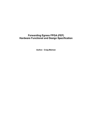
  • 7. CFC Egress FPGA HW Spec. Revision 1.0 02/18/16 Page 7 of 45 Frame Size (Bytes) SustainableBandwidth (%) 64 128 50 100 Buffer Size = 128 Bytes 256 384 512 640 768 896 60 70 80 90 Figure 1 - Frame Buffer Throughput Sawtooth 2.4.3 Scheduler Performance Analysis The scheduler is responsible for allocating 2Gbps of bandwidth amongst all the potential output ports. Since a minimum sized frame is 64 Bytes, this is the scheduler credit granularity. This means that the scheduler has a timeslot tick every 256 nS (64*(1/(2x10 9 /8)) where 64 is number of Bytes, 2x10 9 is 2Gbps and 8 is number of bits per Byte). To insure scheduler accuracy the clock cycle time must divide evenly into 256 nS. A frequency of 140.625 MHz which has a cycle time of 7.111 nS meets this criterion. In this case we have a scheduler timeslot of 36 cycles (36 x 7.111 = 256 nS). 3 Functional Specification 3.1 Functional Overview The FEF is a Xilinx Virtex II Pro FPGA that performs the Egress portion of the forwarding logic in the HOP chassis. This logic consists of the following major functional blocks: 1. Buffer Management: Handles the enqueing and dequeing of the frame data (for both Unicast and Multicast frames), maintains the required data structures (Pointer Table, Queue Table and Frame State Table) and maintains the free buffer pool. 2. Queue Management: Handles the Active Queue Management for the HOP making enqueue/drop decisions using the Random Early Detection (RED) algorithm. 3. Scheduler: Makes frame dequeue decisions using a rate-based scheduling algorithm, “Shaped Deficit Round Robin”. The following block diagram shows the major blocks of the FEF:
  • 8. CFC Egress FPGA HW Spec. Revision 1.0 02/18/16 Page 8 of 45 CFC Egress FPGA (FEF) Queue/Buffer Management (QBM) Scheduler (SCH) Frame Buffer I/F Frame Buffer DDR SDRAM 16M x 64 PIO I/F Pointer Table 2M x 36 Frame State Table 2M x 36 Queue Table 512k x 36 Egress Backpressure via Ingress FPGA Queue Manager (Congestion Control) Table I/F FLC Egress FPGA Block Diagram C Maiman 12/17/2004 16 + 2 8 To ILC's via FIF 16 + 2 66~25 10 Clocks & Resets ~4 Drop Stats (STAT) Pre-Processor (PREP) PMP MCast Lookup Decap Post-Processor (POSTP) Encap Port Translate 97 96 97 36 WD 36 RD 19 A 6 C Scheduler Table 512k x 36 97 Flow Scheduler Port Scheduler FES/FTS Maintenance QT(SVI)forIngressBPPort From Ingress FPGA (FIF) 36 WD 36 RD 18 A 6 C 36 WD 36 RD 19 A 6 C 36 WD 36 RD 18 A 6 C Buffer Manager Enqueue Dequeue Free Buffer ManagerDispatch Return Multicast Staging Block Return LLP HA Figure 2 - CFC Egress FPGA Block Diagram The flow starts with the Pre-Processor (PREP) module which contains the PMP (Point-to-Multipoint) Multicast lookup and the Decap logic which removes any parts of the Invento proprietary Switching Header (defined elsewhere) which are not needed further down the pipeline. The frames continue onto the Queue/Buffer Management (QBM) module which is responsible for enqueing the frame and updating the associated tables. The Scheduler (SCH) is informed of newly enqueued frames by the QBM and using a Shaped Deficit Round Robin scheduling algorithm decides on the next frame to dispatch. The QBM receives these dequeue commands from a command FIFO and reads out the frame from the Frame Buffer. From the QBM the frame enters the Post-Processor (POSTP) module which translates the Destination Port number to the egress slot number. It is then encapsulated with the Invento Interface Header for transmission. The frame is output over a 16 bit datapath (plus 2 bits of control) to the Ingress FPGA where it is steered to the appropriate ILC.
  • 9. CFC Egress FPGA HW Spec. Revision 1.0 02/18/16 Page 9 of 45 The FPGA internals and all interfaces will run synchronously at 140.625 MHz. 3.2 Decap & PMP Multicast Lookup (PREP Module) The Pre-Processing Module does the initial processing on the incoming frame. It examines the frames header and decides what actions to take, including lookups, drops and recognizing learning type frames. Frames arrive over a 16 bit data plus 2 bit control bus from the Ingress FPGA. The 2 bits of control will be encoded as follows (note grey coding): 00  Idle 01  Start of Frame (SOF) 11  Middle of Frame (MOF) 10  End of Frame (EOF) The format of the incoming Switching Header is as follows (note that the table also shows the Ethernet MAC Destination and Source Addresses which are not part of the Invento Header): Table 1 - Switching Header Format & Sequencing DATA CTL D15 D14 D13 D12 D11 D10 D9 D8 D7 D6 D5 D4 D3 D2 D1 D0 VER[1:0] TYPE[2:0] COLOR[1:0] VST PMPID[7:0] SOF VIT RSRVD LEN[10:0] MOF DVI[15:0] MOF SVI[15:0] MOF MAC DEST ADDR [47:40] MAC DEST ADDR [39:32] MOF MAC DEST ADDR [31:24] MAC DEST ADDR [23:16] MOF MAC DEST ADDR [15:8] MAC DEST ADDR [7:0] MOF MAC SOURCE ADDR [47:40] MAC SOURCE ADDR [39:32] MOF MAC SOURCE ADDR [31:24] MAC SOURCE ADDR [23:16] MOF MAC SOURCE ADDR [15:8] MAC SOURCE ADDR [7:0] MOF The fields are defined as follows:
  • 10. CFC Egress FPGA HW Spec. Revision 1.0 02/18/16 Page 10 of 45 Table 2 - Switching Header Field Definitions Field Definition VER Header Version (Initially 0) TYPE Value Definition Where Valid Comments 0 Interface Ingress ILC  CFC FEF should not rcv. 1 Interface Egress CFC  ILC FEF  FIF (Within CFC) FEF should not rcv. 2 Switching FIF  FEF (Within CFC) FEF  FIF (Within CFC) FEF sends if CPU dest. 3 BP Only Header ILC  CFC CFC  ILC FEF should not rcv. 4-7 Reserved COLOR Color (From ILC Policing) 0: Green 1: Yellow (Not currently used) 2: Red 3: Drop (Not currently used) VST Virtual Switch Type: 0: PTP 1: PMP PMPID Point-to-MultiPoint Identifier VIT Virtual Interface Type: 0: Type 0 (How’s that for generic? ;-) 1: Type 1 RSRVD This field used to be OUTMAP, defined as follows  Output Bitmap: Bit 3: CFC3 Bit 2: CFC2 Bit 1: CFC1 Bit 0: CFC0 LEN Frame Length in Bytes (Not including Invento Header) DVI Destination Virtual Interface SVI Source Virtual Interface The PREP Module handles the frame differently for different incoming frame types. The actions are captured in the following table: Table 3 - PREP Module Actions Type Field VST Field DVI Field Action Switching PMP Not all 1’s Normal Unicast Switching PMP All 1’s Normal Multicast, Lookup in EDT with PMP ID Switching PTP Not all 1’s Normal Unicast Switching PTP All 1’s Drop Interface X X Drop Flow Ctl X X Drop Reserved X X Drop If the frame is PMP type (Point-to-MultiPoint) as indicated by the Header VS Type field and the Header’s DVI field is all 1’s then a lookup is performed in the PMP EDT (Egress Destination Table). This is a 256 entry by 32 bit wide internal table. The table is addressed by the 8 bit PMP ID field from the Switching Header. The format of this table is as follows:
  • 11. CFC Egress FPGA HW Spec. Revision 1.0 02/18/16 Page 11 of 45 Table 4 - PMP Egress Destination Table Data Field Bits Mnemonic Description 31:24 RSRVD Reserved 23:8 DESTQ[15:0] Destination Queue – First Queue in chain to be enqueued 7 RSRVD Reserved 6:0 DEG[6:0] Degree – Number of Virtual Switch legs served by this CFC for this PMP ID The details on the use of these fields are discussed in the Enqueing section. The Decap module removes the fields of the Switching Header that are not required downstream within the FEF and constructs an updated header. The format of the updated frame header sent to the QBM is as follows: Table 5 - PREP to QBM Header Format & Sequencing DATA Arrival OrderD15 D14 D13 D12 D11 D10 D9 D8 D7 D6 D5 D4 D3 D2 D1 D0 RSRVD TYPE[2:0] COLOR[1:0] VST - DEGREE[6:0] (Set to 1 for Unicast case) 1 VIT RSRVD LEN[10:0] 2 DESTQ[15:0] (Is DVI for Unicast Case) 3 SVI[15:0] 4 3.3 Queue and Buffer Management (QBM Module) This module is responsible for the enqueing and dequeing of the frames. It has interfaces to 4 external memories:  Frame Buffer – 128MB of DDR SDRAM arranged as 16M x 64 bits (Logically 1M x 128 Bytes).  Pointer Table – 72Mb of SSRAM arranged as 2M x 36 bits (Logically 1M x 64 bits).  Frame State Table – 72Mb of SSRAM arranged as 2M x 36 bits (Logically 1M x 64 bits).  Queue Table – 9Mb of SSRAM arranged as 512k x 36 bits (Logically 64k x 128 bits). The QBM is subdivided into the following functional blocks:  Queue Manager – Responsible for drop decisions when enqueing  Enqueue – Handles the enqueue sequencing for both Unicast and the 1 st enqueing of a Multicast frame  Multicast Staging Block – Handles the enqueing of multicast frames after the 1 st  Dequeue – Handles the dequeue sequencing under the command of the Scheduler  Free Buffer Manager – Maintains the free buffer pool  Table Interface – Handles the interfaces to the Pointer Table, Frame State Table and the Egress Queue Table  DDR SDRAM Interface – Handles the Frame Buffer Interface 3.3.1 Queue Management (Congestion Control) The Queue Management logic determines whether a frame can be enqueued or should be dropped. It does this using an algorithm known as Dynamic Threshold which uses criteria such as
  • 12. CFC Egress FPGA HW Spec. Revision 1.0 02/18/16 Page 12 of 45 Frame Length, Frame Color, Q Length, Q Threshold, Free Buffer Length (FBS) and Free Threshold Size (FTS). FES or Free Excess Size is simply FBS – FTS. This module can generate flow control frames under certain circumstances. The following pseudo-code details the Dynamic Threshold algorithm (as defined in “QoS: Forwarding Architecture” by Santosh Krishnan) [Note: The BP Sets and Releases below are for Ingress Backpressure to the Ingress ILC) [NOTE: This will be changing…]: if (FBS >= Frame Length) { if (Queue Length + Frame Length <= Threshold) { if (FTS >= Frame Length) { Release Full BP for SVI // re-set Green Backpressure (FC-2) for source VI FST.indicator = Threshold // bit QMIND set to 0 in Frame State Table FBS -= Frame Length FTS -= Frame Length Enqueue frame } else { // Process as if the frame was Red RT = Threshold + Alpha[class]*FES if (Queue Length + Frame Length <= RT) { Release Full BP for SVI// re-set Red Backpressure (FC-2) for source VI FST.indicator = Excess // bit QMIND set to 1 in Frame State Table FBS -= Frame Length FES -= Frame Length Enqueue frame } else { Set Out-of-Profile BP for SVI // Set Red Backpressure (FC-2) for source VI Drop frame } } } else { // Queue exceeds threshold if ((Green Frame) && (FTS >= Frame Length)) { // Compliant frame Set Full BP for SVI // set Green Backpressure (FC-2) signal for source VI FST.indicator = Threshold FBS -= Frame Length FTS -= Frame Length Enqueue frame } else { // same as the Red processing above RT = Threshold + Alpha[class]*FES if (Queue Length + Frame Length <= RT) { Release Full BP for SVI // re-set Red Backpressure (FC-2) for source VI FST.indicator = Excess FBS -= Frame Length FES -= Frame Length Enqueue frame } else { Set Out-of-Profile BP for SVI // Set Red Backpressure (FC-2) for source VI Drop frame } } } } else { // Something really bad, like really bad suburban chinese food. China town is better. } The Free Buffer Size and Free Threshold Size Registers are initially set by software and are formatted as follows: Table 6 - Register: FEF_QBM_FBS Data Field Bits Mnemonic Description 31:24 RSRVD Reserved 23:0 FBS[23:0] Free Buffer Size – Set by software on boot to the free buffer size in pages (1M).
  • 13. CFC Egress FPGA HW Spec. Revision 1.0 02/18/16 Page 13 of 45 Table 7 – Register: FEF_QBM_FTS Data Field Bits Mnemonic Description 31:24 RSRVD Reserved 23:0 FTS[23:0] Free Threshold Size – Set by software on boot to the sum of the configured thresholds of the queues. Table 8 – Alpha Table Data Field Bits Mnemonic Description 31:x RSRVD Reserved x:0 ALPHA[x:0] Alpha – Per class dynamic threshold parameter. Higher alpha implies aggressive buffer sharing. Software must ensure that Alpha x FES never exceeds the maximum individual queue length that we can tolerate. If the congestion logic indicates that an Ingress Backpressure signal must be generated then the following sequence of events occurs in the FEF: 1. Lookup in QT using SVI to obtain associated port. 2. Send port and BP Type indication to POSTP module to lookup associated Slot using both Local Link Protect Table and High Availability Table. 3. Queue up Ingress Backpressure (IBP) signal to be sent to the offending Ingress ILC. 3.3.2 Data Structures & Buffer Management The data structures required to meet the needs of HOP’s shared memory architecture are as follows: Queue Table, Frame Buffer, Pointer Table, Frame State Table and the Free Buffer Queue. The frames as stored in pages of 128 Bytes each which can be located anywhere within the Frame Buffer. The location of these frame pages are pointed to by a linked list in the Pointer Table. The page locations are dispensed by the Free Buffer Manager. The list of Queues is maintained in the Queue Table and the Frame State Table contains miscellaneous information related to each frame page. The following diagram shows the relationships between the various tables for the simple Unicast case:
  • 14. CFC Egress FPGA HW Spec. Revision 1.0 02/18/16 Page 14 of 45 CFC Egress Data Structures Queue Table Pointer Table Frame State Table Frame Buffer H QLEN NXQ QTH ACT PRT MC FL FLT SVI T NXTCUR DVI (Q#) Frame/Page 1/1 1/2 3/1 2/1 Frame Payload Frame Payload Frame Payload Frame Payload Unicast Case FLC Egress Data Structures C Maiman 12/14/2004 101 112 210 341 101 210 4 101 112 112 341 210 341 210 101 112 210 341 101 112 210 341 Free Buffer Q Pointers H T Length Free Buffer Dispatch Free Buffer Return Null Dequeue from Head of Free Buffer Queue Enqueue to Tail of Free Buffer Queue H : Queue Head Pointer QLEN : Queue length in pages NXQ : Next Queue (For Multicast) QTH : Queue threshold (For drop ctl) ACT : Action... PRT : Port associated with this DVI (Q) T : Queue Tail Pointer (Last Page of last frame) NXT : Next Pointer CUR : Current Pointer MC : Multicast Count FL : Frame Length (Pages or Bytes) FLT : Frame Length Type SVI : Source Virtual Interface 11 1 1 1 1 2 n n n P B B B Figure 3 - CFC Egress Data Structures (Unicast Case) The following diagram shows a multicast case where the Source VI is handled by this CFC:
  • 15. CFC Egress FPGA HW Spec. Revision 1.0 02/18/16 Page 15 of 45 Note: In this case MC for 210 initially written with DEG = 3. Changed to 2 when it is discovered that SVI is handled by this FLC. Each Q (DVI) written is compared to SVI. Don't write the Q = SVI. CFC 2 CFC Egress Data Structures Queue Table Pointer Table Frame State Table Frame Buffer H QLEN NXQ QTH ACT PRT MC FL FLT SVI T NXTCUR DVI (Q#) Frame/Page 1/1 1/2 3/1 2/1 Frame Payload Frame Payload Multicast Frame Payload Frame Payload Multicast Case 1 FLC Egress Data Structures C Maiman 12/14/2004 101 112 210 341 101 210 4 101 112 112 341 210 341 210 101 112 210 341 101 112 210 341 Free Buffer Q Pointers H T Length Free Buffer Dispatch Free Buffer Return Null Dequeue from Head of Free Buffer Queue Enqueue to Tail of Free Buffer Queue H : Queue Head Pointer QLEN : Queue length in pages NXQ : Next Queue (For Multicast) QTH : Queue threshold (For drop ctl) ACT : Action... PRT : Port associated with this DVI (Q) T : Queue Tail Pointer (Last Page of last frame) NXT : Next Pointer CUR : Current Pointer MC : Multicast Count FL : Frame Length (Pages or Bytes) FLT : Frame Length Type SVI : Source Virtual Interface 422 422 1 42 42 422 210 Null 422 Empty 422 Null 2 n n n P B B B 11 1 1 2 1 VS 99 VI = 7 VI = 9 VI = 23 CFC 1 Case 1 Returned to free buffer pool when MC dec. to 0 Returned to free buffer pool when buffer consumed. Empty Figure 4 - CFC Egress Data Structures (Multicast Case 1) The following diagram shows a multicast case where the Source VI is handled by the other CFC (NOTE: This scenario cannot occur in Release 1 of the hardware since there can only be one active CFC in a system, so all frames are handled by the active CFC):
  • 16. CFC Egress FPGA HW Spec. Revision 1.0 02/18/16 Page 16 of 45 CFC 1 Note: In this case MC for 210 initially written with DEG = 2. CFC 2 CFC Egress Data Structures Queue Table Pointer Table Frame State Table Frame Buffer H QLEN NXQ QTH ACT PRT MC FL FLT SVI T NXTCUR DVI (Q#) Frame/Page 1/1 1/2 3/1 2/1 Frame Payload Frame Payload Multicast Frame Payload Frame Payload Multicast Case 2 FLC Egress Data Structures C Maiman 12/14/2004 101 112 210 341 101 210 4 101 112 112 341 210 341 210 101 112 341 101 112 210 341 Free Buffer Q Pointers H T Length Free Buffer Dispatch Free Buffer Return Null Dequeue from Head of Free Buffer Queue Enqueue to Tail of Free Buffer Queue H : Queue Head Pointer QLEN : Queue length in pages NXQ : Next Queue (For Multicast) QTH : Queue threshold (For drop ctl) ACT : Action... PRT : Port associated with this DVI (Q) T : Queue Tail Pointer (Last Page of last frame) NXT : Next Pointer CUR : Current Pointer MC : Multicast Count FL : Frame Length (Pages or Bytes) FLT : Frame Length Type SVI : Source Virtual Interface 422 422 1 42 42 422 210 Null 422 Empty 422 Null 2 n n n P B B B 11 1 1 2 1 VS 99 VI = 3 VI = 9 VI = 23 Case 2 210 Returned to free buffer pool when MC dec. to 0 Returned to free buffer pool when buffer consumed. Empty Figure 5 - CFC Egress Data Structures (Multicast Case 2) The Frame Buffer enqueing and dequeing algorithms are covered in the Enqueing and Dequeing sections below. 3.3.2.1 Frame Buffer The Frame Buffer is the shared memory for the queuing of frames in transit through the HOP chassis. The Frame Buffer is a 128MB DDR SDRAM physically organized as 16M x 64 bits. It is logically organized as 1 million entries of 128 Bytes each. The 128 Byte block is called a page and is the minimum memory allocation for a frame. Frames larger than 128 Bytes will use multiple pages which may be located anywhere within the Frame Buffer. The Pointer Table maintains the linked list of pages. All transactions with the Frame Buffer will be in bursts of 16 words. This is 8 FPGA cycles since the SDRAM is Double Data Rate.
  • 17. CFC Egress FPGA HW Spec. Revision 1.0 02/18/16 Page 17 of 45 The SDRAM will run at 140.625 MHz synchronously with the FPGA. 3.3.2.2 Pointer Table The Pointer Table maintains the linked list pointers to the pages in the Frame Buffer. This memory will be an external 72Mb Dual Port QDR SSRAM physically organized as 2M Words x 36 bits. Logically the memory will be 1 million entries of 64 bits each. This will give us many spare bits for increasing the buffer size. Each entry consists of two fields: Current Pointer (CUR) and Next Pointer (NXT). Each is 20 bits in order to address 1 Million Frame Buffer Pages. Normally a linked list would not require a current pointer, but as will be shown later it can be used effectively for multicast frames. In order to maintain a queue of free pages software must initialize the Pointer Table as follows (NOTE: Last entry should have the next field set to NULL: All 0’s):  PT[CUR](n)  n Note: Indicates Pointer Table CUR field at address n  PT[NXT](n+4)  n+8 The memory will run at 140.625 MHz synchronously with the FPGA. The format of the Pointer Table is as follows (data bits in parentheses are software view): Table 9 - Pointer Table Data Field Bits Mnemonic Description 63:52 (W1: 31:20) RSRVD Reserved 51:32 (W1: 19:0) NXT[19:0] Current Pointer – Points to the frame page in the Frame Buffer and Frame State Table 31:20 (W0: 31:20) RSRVD Reserved 19:0 (W0: 19:0) CUR[19:0] Next Pointer – Points to the next Pointer Table entry 3.3.2.3 Frame State Table The Frame State Table is an external 72Mb Dual Port QDR SSRAM physically organized as 2M Words x 36 bits and used for storing various data associated with each memory page in the Frame Buffer. It is logically organized as 1 Million entries of 64 bits each. The Frame State Table is organized as follows (data bits in parentheses are software view): Table 10 - Frame State Table Data Field Bits Mnemonic Description
  • 18. CFC Egress FPGA HW Spec. Revision 1.0 02/18/16 Page 18 of 45 Data Field Bits Mnemonic Description 63:43 (W1: 31:11) RSRVD Reserved 42:32 (W1: 10:0) FRAME_LEN[10:0] Frame Length in Bytes 31 (W0: 31) RSRVD Reserved 30:24 (W0: 30:24) MC[6:0] Multicast Count – Indicates the number of output queues this frame is queued on. Set to 1 for Unicast frames or loaded from Degree field of PMP Egress Destination Table for multicast (will be decremented by 1 if it is found that the Source is handled by this CFC). This field is decremented by 1 for each dequeue. When this reaches 0, this page is returned to the free buffer queue. 23:19 (W0: 23:19) RSRVD Reserved 18 (W0: 18) LAST If Set to 1 indicates that this is the last page of the frame, otherwise more to go. 17 (W0: 17) VIT Virtual Interface Type. 16 (W0: 16) QMIND Queue Manager Indicator – If set indicates that this was enqueued with Excess space otherwise indicates that the frame was within Threshold. 15:0 (W0: 15:0) SVI[15:0] Source Virtual Interface – Indicates the source of the queued frame. Set from the frame header. The Multicast Count Field is set to 1 for Unicast frames and initially set from the Degree field of the PMP Egress Destination Table for Multicast frames. Once the multicast frame is placed on all the destination queues this field may be decremented by one if the Source was found to be serviced by this CFC. This is discovered by comparing the queue number (Destination VI) of each queue it’s being placed on against the Source VI of the frame. If there is a match then the frame is not placed on that queue and the MC Field of the first queue it’s placed on will be decremented by one. Software need not initialize this memory. The memory will run at 140.625 MHz synchronously with the FPGA. 3.3.2.4 Queue Table The Queue Table is an external 18Mb Dual Port QDR SSRAM physically organized as 512k Words x 36 bits and used for maintaining the queue information. It is logically organized as 64k entries of 128 bits each. The Table is organized as follows (data bits in parentheses are software view): Table 11 - Queue Table Data Field Bits Mnemonic Description
  • 19. CFC Egress FPGA HW Spec. Revision 1.0 02/18/16 Page 19 of 45 Data Field Bits Mnemonic Description 127:123 (W3: 31:27) RSRVD Reserved 122:117 (W3: 26:21) BACKUPPORT[5:0] If “Use Backup VI” action bit is set then use this Port for header in outgoing dequeued frames. 116:101 (W3: 20:5) BACKUPVI[15:0] If “Use Backup VI” action bit is set then use this VI for header in outgoing dequeued frames. 100:96 (W3: 4:0) QTH[4:0] Queue Threshold – Used by the Queue Manager to determine whether a frame will actually get enqueued. Initialized by SW on boot (may also be changed by SW realtime). Indirection to a table of 32 different possible queue thresholds? 95 (W2: 31) RSRVD Reserved 94:75 (W2: 30:11) HEAD[19:0] Head Pointer – This points to the first frame in the queue. Points to the Pointer Table which points to the actual location in the Frame Buffer. Initialized to 0 by SW on boot. 74:55 (W2: 10:0) (W1: 31:23) TAIL[19:0] Tail Pointer – This points to the last page of the last frame in the queue. Points to the Pointer Table which points to the actual location of the last page of the last frame in the Frame Buffer. Initialized to 0 by SW on boot. 54:28 (W1: 22:0), (W0: 31:28) QLEN[26:0] Queue Length – The length in bytes of the queue. Initialized to 0 by SW on boot. 27:12 (W0: 27:12) NXQ[15:0] Next Queue – Points to the next queue in the chain of queues for multicast groups. Initialized by SW on boot (may also be changed by SW realtime). 11:10 (W0: 11:10) CLASS[1:0] Class of Service Level 9:6 (W0: 9:6) ACT[4:0] Action: [4] – Reserved [3] – Use Backup VI [2] – Check Type [1] – VI Type (0  Type 0, 1  Type 1) [0] – CC destined VI 5:0 (W0: 5:0) PORT[5:0] Port – Output Port associated with this queue. Initialized by SW on boot. The memory will run at 140.625 MHz synchronously with the FPGA. 3.3.3 Enqueing The following sections detail the procedures for the enqueing of frames into the Frame Buffer. 3.3.3.1 Unicast & Multicast 1st Queue The QBM receives a frame from the PREP module and precedes to enqueue it. It does this for both Unicast frames and the 1 st queue of a Multicast frame. For Multicast, once it has enqueued the frame into the first queue it pushes an information block into the Multicast Staging Queue (MSQ). The MSQ engine upon seeing an entry will start the process of enqueing the frame on all the other queues in the Multicast group. For all the following pseudo-code the following abbreviations apply: FB = Frame Buffer, PT = Pointer Table, FST = Frame State Table and QT = Queue Table. An example would be: QT[qlen](dvi)  This indicates the QLEN field of the Queue Table at address dvi. FHDR means Frame Header as passed from the PREP module. The following pseudo-code details the enqueing of a frame into the Frame Buffer:
  • 20. CFC Egress FPGA HW Spec. Revision 1.0 02/18/16 Page 20 of 45 Notes:  In the case of Multicast, if the first queue query to the queue manager gets a drop response, then the frame is dropped completely. Subsequent queues are not checked. This is done because the enqueuer could get backed up while it checks all the queues in the multicast chain (they could ALL receive drop responses).  The sequencer does not start to operate on a frame until at least 1 page is in the incoming FIFO (with the exception of a frame which is less than 1 page in size).  All arithmetic operations must be performed as atomic Read-Modify-Writes to avoid race conditions with other modifying processes. This may require a second read in order to reduce lock time (e.g. Queue Table queue length modification). This will be handled by issuing Read with Lock to the Interface Logic.  Some of the actions may be done in parallel. next_free  Pop FREE_Q_DISPATCH_FIFO // Get 1st free address frame_head  next_free // Use later to update old Q tail num_pagesx  FHDR[len[10:7]] // Shift for calc of # pages frame_len_bytes  FHDR[len] // Total frame length in Bytes qt_temp  QT(FHDR[destq]) // Read QT at address destq (dvi) destqx  FHDR[destq] // Modifiable copy degreex  FHDR[degree] // ditto cbuffer_idx  0 // Init for multicast cbuffer idx if (|FHDR[len[6:0]]) { // Spills to a next page frame_len_pages  num_pagesx + 1 } else { // Exactly on page boundary frame_len_pages  num_pagesx } num_pages  frame_len_pages // Need local copy to decrement // Source Equal Destination Check if ((destqx == FHDR[svi]) && degreex == 1) drop_uni  1 // Source eq Dest else if (destqx == FHDR[svi]) { // MC Case of skip 1st destqx  qt_temp[nxq] // What’s the Next Queue? qt_temp  QT(destqx) // Read QT @ Next Queue degreex  degreex – 1 // 1 less to do } // Split Horizon Type Check if ( degreex > 1 && qt_temp[act[chk_type]] && (act[vi_type] == FHDR[vit])) { drop_on_type_chk  1 // Broadcast, check type and type } else { // matches ok_to_q  QMAN(frame_len_bytes, qt_temp[qlen,qth,class], FHDR[color]) // Query Q Manager qmind  QMAN // Did Q Man use excess space? } if (ok_to_q && !drop_uni && !drop_on_type_chk) { // Good to go? done  0 // Init done while (!done) { // More? cur_entry  next_free if (num_pages == 1) { // Is the remaining frame <= 128B? last_bit  1 // FST’s LAST bit – Last page! PT(cur_entry)  cur_entry, NULL // Write PT(new entry): cur, nxt Done  1 // Done! } else { // It’s more than 1 page (> 128B) last_bit  0 // FST LAST bit – More pages! next_free  Pop FREE_Q_DISPATCH_FIFO // Get an address for the next page PT(cur_entry)  cur_entry, next_free // Write PT(last_entry): cur, nxt } FB(cur_entry)  F(block) // Write FB with block from FIFO // Write FST: mc,etc. FST(cur_entry)  degreex, FHDR[vit, svi],frame_len_bytes,last_bit,qmind num_pages  num_pages – 1 // Did a page // Write Circular Buffer with FB Pointers for multicast staging logic
  • 21. CFC Egress FPGA HW Spec. Revision 1.0 02/18/16 Page 21 of 45 if (degreex > 1) { // Multicast cbuffer(cbuffer_wr_ptr + cbuffer_idx)  cur_entry cbuffer_idx  cbuffer_idx + 1 } } // Append our new frame to the end of the queue pt_old_cur  PT[cur](qt_temp[tail]) // Read PT(old tail): cur PT(qt_temp[tail])  pt_old_cur,frame_head // Write PT(old tail): cur, nxt qt_temp  QT(destqx) // Read Lock QT new_q_len  qt_temp[qlen] + frame_len_bytes // Calculate new Q length QT(destqx)  qt_temp[head], cur_entry, new_q_len, qt_temp[nxq], qt_temp[qth], qt_temp[act], qt_temp[port] // Write QT(destqx) SCH  destqx, frame_len_bytes, qt_temp[port], qt_temp[class] // Post to Sched If (degreex > 1) { // Push Multicast Staging Queue MSQ  qt_temp[nxq], FHDR[svi], frame_len_bytes, FHDR[color], FHDR[vit] Move cbuffer_wr_ptr by frame_len_pages } } else { Drop whole frame // Drain whole frame from input FIFO FREE_Q_RETURN_FIFO  Push next_free // Return next_free to Free Buf } Manager If the frame to be written is less than or equal to 128 Bytes then the following minimum number of logical accesses will occur (note that some of these can occur in parallel):  Read QT Get Info _  Write PT Write Pointer to Block |  Write FST Write Block Info |--- Inner Loop  Write FB (16 words) Write Block to Frame Buffer _|  Read PT Read Old Tail  Write PT Write Old Tail with pointer to new frame’s first block  Read Lock QT Read with Lock  Write QT Write QT with new tail pointer to new frame’s last block and new Q length in pages In summary: QT: 3 accesses (R, R(Locked), W), FB: 16 write burst (8 cycles), PT: 3 accesses (W, R, W) and FST: 1 access (W). The Queue Table requires 2 accesses for each logical access so the 3 logical accesses equals 6 physical access cycles. For every block that is queued a free page must be dequeued from the free buffer queue. This takes one additional access to the PT to read the current free Q head’s nxt pointer (done by Free Buffer Manager). So the total cycle count for the enqueing of a single minimum size frame we have: Table 12 - Enqueue Physical Memory Cycle Counts Memory Access Cycles QT 6 FB 8 PT 4 FST 1 Once the frame is completely enqueued the Scheduler is sent a block of data about the frame. This data consists of the following information:  Queue Number From header DESTQ (DVI) field  Queue Length Length in pages. From Queue Table
  • 22. CFC Egress FPGA HW Spec. Revision 1.0 02/18/16 Page 22 of 45  Queue Threshold From Queue Table  Frame Length Length in Bytes from header Length field  Frame Color From header Color field 3.3.3.2 Multicast Staging Block When the QBM encounters a multicast frame the enqueing engine proceeds by enqueing the entire frame, as shown above, in the 1 st queue as indicated by the PMP Egress Destination Table (unless the SVI equals this Queue number). Information is then placed in the Multicast Staging Queue (MSQ) for subsequent enqueing onto the remaining queues. The Multicast Staging Block is responsible for this enqueing. It operates independently of the main enqueing engine. Each 45 bit MSQ entry is formatted as follows: DESTQ[15:0] SVI[15:0] FRAME_LEN[10:0] COLOR VIT The MSQ is 16 entries deep, which enables the staging of 16 multicast frames. The fields are defined as follows: Table 13 - Multicast Staging Queue Field Definitions Field Definition DESTQ This is the 2nd queue that the frame will be enqueued on. The 1st was already done. This field was extracted from the NXQ field from the Queue Table entry of the 1st queue. SVI Source Virtual Interface from the header of the frame. FRAME_LEN Indicates the length of the frame in Bytes. COLOR Indicates the color of the frame (1 = Green, 0 = Red) VIT Virtual Interface Type There is one entry for each frame to be queued. The following diagram helps explain the procedure for enqueing a multicast frame. Note that the views of the frames in the queues do not directly represent Frame Buffer memory, but a schematic view of the queues.
  • 23. CFC Egress FPGA HW Spec. Revision 1.0 02/18/16 Page 23 of 45 1st Queue Dest Queue Head Tail 1 2 3 4 5 6 7 8 12 9 13 10 14 11 15 Previous frame data in queue Pg. 1 of frame Pg. 2 of frame Pg. 3 of frame Frame completely written in 1st queue by main Enqueing Engine Numbers represent order of writing Next Q Next Q Next Q Next Q Remaining frames (pointers only, not data) enqueued by Multicast Staging Enqueing Engine. NULL Note that the frame data itself is only written to the Frame Buffer once, on the first queue by the main enqueing engine. All subsequent queues written only write the Pointer Table with pointers to the original data in the Frame Buffer. This can be seen in the earlier diagrams of the Data Structures. When the Multicast Staging Engine sees an entry in the MSQ it starts the process of enqueing the remaining frames. The logic is similar to the main enqueing engine: Reading the Queue Table, comparing the SVI and the DestQ to see if we should skip the frame, checking with the Queue Manager to see if we can enqueue this frame and then starting the enqueue process. A circular buffer is maintained (cbuffer) which has the list of Frame Buffer pointers to the original frame. This is a 128 entry buffer (by 20 bits) with a read pointer and write pointer. The main enqueing engine writes this (starting at the write pointer) with all of the Frame Buffer pointers (up to 16) for each frame loaded into the MSQ. The Multicast Staging Block reads this buffer using a read pointer that it maintains. Both pointers are reset to zero on boot. When this logic starts to process a newly staged frame it will read through all the Frame Buffer pointers for the frame for each queue it is enqueing upon. When it is done with all the enqueing, then it moves the read pointer to the next frame entry. See the following diagram:
  • 24. CFC Egress FPGA HW Spec. Revision 1.0 02/18/16 Page 24 of 45 Frame 1 Frame 2 Frame 3Frame 3 con't cbuffer_rd_ptrcbuffer_wr_ptr pg 1 ptr pg 2 ptr pg 3 ptr pg 1 ptr pg 2 ptr pg 3 ptr pg 1 ptr pg 2 ptr pg 3 ptr pg 4 ptr pg 4 ptr pg 5 ptr pg 6 ptr pg 7 ptr pg 8 ptr pg 9 ptr pg 10 ptr pg 11 ptr pg 12 ptr Empty Region Queue X Queue Y Queue Z cbuffer_idx Queue W Figure 6 - Multicast Staging Logic Circular Buffer The following pseudo-code details the Multicast Staging Enqueue Engine. Notes:  All arithmetic operations must be performed as atomic Read-Modify-Writes to avoid race conditions with other modifying processes. This may require a second read in order to reduce lock time (e.g. Queue Table queue length modification). This will be handled by issuing Read with Lock to the Interface Logic.  Some of the actions may be done in parallel.  cbuffer_rd_ptr is the pointer into the circular buffer containing the pointers to the original frame data in the Frame Buffer for the next frame to be processed. msqt  Pop MSQ // Get the info from the MSQ next_free  Pop FREE_Q_DISPATCH_FIFO // Get 1st free address frame_head  next_free // Use later to update old Q tail frame_len_bytes  msqt[frame_len] // Use later… num_pagesx  msqt[frame_len[10:7]] // Shift for calc of # pages destqx  msqt[destq] // Modifiable copy if (|msqt[frame_len[6:0]]) { // Spills to a next page frame_len_pages  num_pagesx + 1 } else { // Exactly on page boundary frame_len_pages  num_pagesx } num_pages  frame_len_pages // Local copy to decrement done_all_queues  0 // Init for new MSQ entry processng while (!done_all_queues) { qt_temp  QT(destqx) // Read QT at address destqx cbuffer_idx  0 // Init the index for the cbuffer cur_fb_ptr  cbuffer(cbuffer_rd_ptr + cbuffer_idx) // Get the 1st pointer to FB if (destqx == msqt[svi]) { // Do we skip? fstx  FST(cur_fb_ptr) // Read FST for mc field fstx[mcx]  fstx[mcx] – 1 // 1 less to do FST(cur_fb_ptr) fstx[mcx], fstx[…] // Write FST: mc, etc. destqx  qt_temp[nxq] // What’s the Next Queue? if (destqx == NULL) { // Done already?? done_all_queues  1 // Waaahhh.. done so soon… } else { qt_temp  QT(destqx) // Read QT @ Next Queue
  • 25. CFC Egress FPGA HW Spec. Revision 1.0 02/18/16 Page 25 of 45 } } // Split Horizon Type Check if ( degreex > 1 && qt_temp[act[chk_type]] && (act[vi_type] == FHDR[vit])) { drop_on_type_chk  1 // Broadcast, check type and type } else { // matches ok_to_q  QMAN(frame_len_bytes, qt_temp[qlen,qth,class], FHDR[color]) // Query Q Manager qmind  QMAN // Did Q Man use excess space? } if (!done_all_queues) { if (ok_to_q && !drop_on_type_chk) { // Good to go? done_all_pages  0 // Init done while (!done_all_pages) { // More pages? cur_entry  next_free if (num_pages == 1) { // Is the remaining frame <= 128B? last_bit  1 // FST’s LAST bit – Last page! PT(cur_entry)  cur_fb_ptr, NULL // Write PT(new entry): cur, nxt done_all_pages 1 // Done with all the pages! } else { // It’s more than 1 page (> 128B) last_bit  0 // FST’s LAST bit – More pages! next_free  Pop FREE_Q_DISPATCH_FIFO // Get an address for the nxt pg PT(cur_entry)  cur_fb_ptr, next_free // Write PT(last_entry): cur, nxt } num_pages  num_pages – 1 // Did a page cbuffer_idx  cbuffer_idx + 1 // Pointer to next entry in cbuffer cur_fb_ptr  cbuffer(cbuffer_rd_ptr + cbuffer_idx) // Get the next pointer to FB } // Append our new frame to the end of the queue pt_old_cur  PT[cur](qt_temp[tail]) // Read PT(old tail): cur PT(qt_temp[tail])  pt_old_cur,frame_head // Write PT(old tail): cur, nxt qt_temp  QT(destqx) // Read Lock QT new_q_len  qt_temp[qlen] + frame_len_bytes // Calculate new Q length QT(destqx)  qt_temp[head], cur_entry, new_q_len, qt_temp[nxq], qt_temp[qth], qt_temp[act], qt_temp[port] // Write QT(destqx) SCH  destqx, frame_len_bytes, qt_temp[port], qt_temp[class] // Post to Sched } } else { // DROP this one!!! fstx  FST(cur_fb_ptr) // Read FST for mc field fstx[mcx]  fstx[mcx] – 1 // 1 less to do FST(cur_fb_ptr) fstx[mcx], fstx[…] // Write FST: mc, etc. FREE_Q_RETURN_FIFO  Push next_free // Return next_free to Free Buf } Manager } if (qt_temp[nxq] == NULL) { // At the end of the chain of Q’s? done_all_queues  1 Move cbuffer_rd_ptr by frame_len_pages } else { destqx  qt_temp[nxq] // Get the next one!! } } The inner loop in the above code is the frame enqueuer which enqueues all the pages of a frame on one queue. The outer loop goes through all the queues that the frame is to be enqueued upon. If the multicast frame to be written is less than or equal to 128 Bytes then the following minimum number of logical accesses will occur (note that some of these can occur in parallel): ______  Read QT Get Info |  Read FST Get MC Field |
  • 26. CFC Egress FPGA HW Spec. Revision 1.0 02/18/16 Page 26 of 45  Write FST Write Back |  Read QT To get next in line Q __ |  Write PT Write Pointer to Block |--Inner Loop |-- Outer Loop  Write PT Write Pointer to Block __| (Frames) | (Queues)  Read PT Read Old Tail |  Write PT Write Old Tail with pointer to new frame’s first block  Read Lock QT Read with Lock |  Write QT Write QT _____| In summary: QT: 4 accesses (R, R, R(Locked), W), PT: 3 accesses (W, W, W) and FST: 1 access (R). The Queue Table requires 2 accesses for each logical access so the 4 logical accesses equals 8 physical access cycles. For every block that is queued a free page must be dequeued from the free buffer queue. This takes one additional access to the PT to read the current free Q head’s nxt pointer (done by Free Buffer Manager). So the total cycle count for the enqueing of a single minimum size frame we have: Table 14 - Multicast Enqueue Physical Memory Cycle Counts Memory Access Cycles QT 8 PT 4 FST 1 3.3.4 Dequeing The QBM receives dequeue commands from the Scheduler via a command FIFO. This command FIFO contains the Queue number from which we should dequeue a frame. Note that all arithmetic operations must be performed as atomic Read-Modify-Writes to avoid race conditions with other modifying processes. This will be handled by issuing Read with Lock to the Interface Logic. The following pseudo-code shows the dequeue procedure for a frame (q_num is the queue number (VI) sent by the Scheduler) (Note that some of the actions may be done in parallel): qt_temp  QT(q_num) // Read QT at q_num sent by SCH pt_ptr  qt_temp[head] pt_temp  PT(pt_ptr) // Read PT at the head of the q fst_temp  FST(pt_temp[cur]) // Read FST pointed to by PT cur FHDR  Construct… // Construct Interface Header. If // “Use Backup VI” action bit is // set, use BU VI & BU Port from // QT. If “CC Destined VI” => // construct Switching Header. done  0 // Init done while (!done) { done  (fst_temp[last] == LAST) // This is the last time around frame_out  FB(pt_temp[cur]) // Read FB page if (pt_ptr != pt_temp[cur]) { // Is this a MCast “helper” ptr? FBM  pt_ptr // Return MCast helper ptr to FBM } else if (fst_temp[mc] == 1) { // Last MC frame or Unicast FBM  pt_ptr } // Else it’s MCast and there are // more to do so don’t give the ptr
  • 27. CFC Egress FPGA HW Spec. Revision 1.0 02/18/16 Page 27 of 45 // back just yet! if (fst_temp[mc] > 1) { mcx  fst_temp[mc] – 1 // We’ve done a MCast so dec mc FST(pt_temp[cur])  mcx, fst_temp[…] // Write FST } pt_ptr  pt_temp[nxt] pt_temp  PT(pt_ptr) // Read Next PT entry fst_temp  FST(pt_temp[nxt]) // Read Next FST entry } qt_temp  QT(q_num) // Read Lock QT new_q_len  qt_temp[qlen] – fst_temp[frame_len] // Calculate new Q length in Bytes QT(q_num)  pt_temp[nxt], qt_temp[tail], new_q_len, qt_temp[nxq], qt_temp[qth], qt_temp[act], qt_temp[port]// Write QT: New Head (nxt) & Len QM  fst_temp[qmind], fst_temp[frame_len] // Tell Q Man whether to inc Free Threshold/Excess Size register if (new_q_len > 0) { length_next_frame  fst_temp[frame_len] // Length of the next frame in Q } else { // Empty Q length_next_frame  0 // We read garbage so force } SCH  q_num, length_next_frame // Tell SCH: Q, length of next frame If the frame to be read is less than or equal to 128 Bytes then the following minimum number of logical accesses will occur (note that some of these can occur in parallel):  Read QT Get Info  Read PT Read Pointer to Block at head of Queue  Read FST Read Block Info  Read Lock QT Read with Lock  Write QT Write QT with new head pointer and new Q length in pages  Read FB Read Frame Buffer In summary: QT: 3 accesses (R, R(Locked), W), FB: 16 read burst, PT: 1 access (R) and FST: 1 access (R). The Queue Table requires 2 physical accesses for each logical access so the 3 logical accesses equals 6 physical access cycles. For every block that is dequeued a free page must be enqueued to the free buffer queue. This entails 2 additional accesses to the PT by the Free Buffer Manager. This is documented in the Free Buffer Manager section. So the total cycle count for the dequeing of a single minimum size frame we have: Table 15 - Dequeue Physical Memory Cycle Counts Memory Access Cycles QT 6 FB 8 PT 3 FST 1 3.3.5 Free Buffer Manager The Free Buffer Manager maintains a linked list of available Frame Buffer pages. The linked list itself resides within the Pointer Table (PT) used by the Frame Buffer. Essentially all the free space
  • 28. CFC Egress FPGA HW Spec. Revision 1.0 02/18/16 Page 28 of 45 in the PT is linked together. The Head, Tail and Queue Length information is maintained as an internal register. See the section on the Pointer Table for initialization information. The format of the Free Buffer Queue Registers is as follows: Table 16 - Register: FEF_QBM_FREEQ_HEAD Data Field Bits Mnemonic Description 31:20 RSRVD Reserved 19:0 HEAD[19:0] Head of Free Buffer Queue in Pointer Table Table 17 - Register: FEF_QBM_FREEQ_TAIL Data Field Bits Mnemonic Description 31:20 RSRVD Reserved 19:0 TAIL[19:0] Tail of Free Buffer Queue in Pointer Table Table 18 - Register: FEF_QBM_FREEQ_LEN Data Field Bits Mnemonic Description 31:20 RSRVD Reserved 19:0 LEN[19:0] Length in pages of Free Buffer Queue in Pointer Table The Free Buffer Manager has an output Dispatch FIFO and an input Return FIFO. The FBM will prefetch free page pointers and push them into the Dispatch FIFO for use by the Buffer Manager. The Dispatch FIFO is 16 words deep by 20 bits wide. The Return FIFO is 16 words deep by 20 bits wide. The hardware will attempt to keep the Dispatch FIFO as full as possible so the Buffer Manager always has a supply. To dequeue a free page from the Free Buffer Queue and place it in the Dispatch FIFO requires the following steps: 1. Read PT(head) to retrieve nxt field (head is from Q Head Register) 2. Push head into Dispatch FIFO 3. Write Q Head Register with nxt To enqueue a free page onto the Free Buffer Queue when one has been returned in the Return FIFO, the following steps are required: 1. Pop New Free Address (NFA) from Return FIFO 2. Write PT(NFA) with cur = NFA and nxt = NULL 3. Write PT(tail) with cur = tail and nxt = NFA (tail is from Q Tail Register) 4. Write Q Tail Register with NFA 3.3.6 Table Interface Block The table interface block handles the interfaces for the following tables: Pointer Table, Queue Table and Frame State Table. All of these are QDR II SSRAM’s.
  • 29. CFC Egress FPGA HW Spec. Revision 1.0 02/18/16 Page 29 of 45 The interfaces are handled separately and each can get requests for access from 5 sources (handled in this priority order): 1. Enqueue Logic 2. Dequeue Logic 3. Multicast Staging Process 4. Queue Manager (Ingress Backpressure SVI lookup to QT only – to get Port #) 5. Free Buffer Manager (only accesses Pointer Table) 6. Software PIO The interface logic must be able to handle Read-Modify-Write situations with some of the tables. This will be handled by the requestor issuing a Read-Lock instead of a simple Read command. This will lock out (hold off) any other requestors to that location until the Read-Lock issuer has issued a write to the same location. This will insure consistent state for fields such as Queue Length (Queue Table) and the Multicast Count (Frame State Table). All the tables are byte parity protected with generation on writes and check on reads. 3.3.7 SDRAM Interface Block The SDRAM interface block handles the interface for the Frame Buffer which is a DDR SDRAM operating synchronously at 140.625 MHz (281.25 MHz effective rate). The interface can get requests from the following 3 sources (handled in this priority order): 1. Enqueue Logic 2. Dequeue Logic 3. Software PIO More more more…. 3.4 Scheduler (SCH Module) The Scheduler gets enqueing information from the Queue/Buffer Manager and makes decisions about what frames to dequeue for transmission. When it makes this decision it pushes a dequeue command into the dequeue command FIFO. The scheduler (and QoS) architecture is discussed in detail in the Internal Memo “QoS: Forwarding Architecture” by Santosh Krishnan. What follows is an architectural summary and details concerning the implementation. The scheduler is divided into two sections: Port Scheduler and Flow Scheduler. The Port Scheduler picks ports according to how bandwidth has been allocated to it. The Flow Scheduler then apportions that ports bandwidth to the VI’s serviced by that port. It first tries to give out guaranteed bandwidth using a “Shaped Deficit Round Robin” scheme else it gives out excess bandwidth using a simple round robin. The following block diagram shows the overall partitioning of the scheduler tables and logic:
  • 30. CFC Egress FPGA HW Spec. Revision 1.0 02/18/16 Page 30 of 45 Flow SchedulerPort Scheduler Fields Current (16) Fields Reserved (xx) Q Length (16) Head Frame Length (11) Credits (16) Offset (?) VI Back Pressure (1) Ready Bit (1) Ready Next Ptr (16) Excess Eligible Next Ptr (16) Excess Eligible Previous Ptr (16) Dispatcher Dequeue Update Controller Port Template Table (double buffered) 2000 x 7b VI Template Region Table (double buffered) 64 x 54b Excess Eligible List Current Pointer Table 64 x 16b Port Backpressure Table 64 x 2b VI Template Table (double buffered) 250,000 x 16b Scheduler Table 64k x 128b 6 18 CurrentPort 16 VI Scheduler Enqueue Update Controller Port Table Traverser Tick VI (16) Frame Length (11) Port (6) VI (16) VI (16) Next Frame Length (11) Port (6) Queue/Buffer Manager Tick TDM Access to Sch Table Apportions 2Gbps of bandwidth in 1Mbps increments amongst 64 ports 2Gbps/1Mbps = 2000 Apportions 2Gbps of bandwidth in 8kbps increments amongst 64k Virtual Interfaces 2Gbps/8kbps = 250,000 Egress Backpressure Flow_Info (7) Flow_Info_Ctl (2) From FLC Ingress FPGA To Scheduler 1 Valid FLC Egress FPGA Scheduler Block Diagram C Maiman 12/23/2004 256nS To Enqueue Update Controller, Dequeue Update Controller & Scheduler Table B Table A Fields VI All 1's => Invalid Table B Table A Fields Port (6) Valid (1) Table B Table A Fields Start (18) Current (18) End (18) Figure 7 - Scheduler Block Diagram 3.4.1 Port Scheduler The whole scheduler operates on a 64 Byte time clock. This is the time it takes to transfer 64 Bytes (this is the granularity of the scheduler) over two GigE lines 2Gbps). This time is 256 nS or 36 cycles using a 140.625 MHz clock. The port scheduler is the source of the timeslot “Tick” for the entire scheduler. The Port Scheduler contains a Port Template Table which apportions 2Gbps of bandwidth amongst the (potentially) 64 ports. The granularity of bandwidth allocation is 1Mbps, so therefore the table has 2000 entries (2B/1M = 2000). The Port Table Traverser starts by pointing to the top entry of the table which contains a port number [5:0] (and a valid bit [6]). If there is a valid port number this indicates that that port gets 1Mbps of bandwidth. After 256 nS the pointer moves to the next entry which contains another (or the same) port number. If it’s the same port number this means that this port has (at least) 2Mbps of bandwidth allocated to it. Note that if this Egress CFC is servicing one GigE port all the entries will have the same port number. The Traverser scans through all the table’s entries and then restarts at the top. The Port Number and Valid bits are sent to the Flow Scheduler.
  • 31. CFC Egress FPGA HW Spec. Revision 1.0 02/18/16 Page 31 of 45 In order for software to update the Port Template Table in a coherent manner the table is double buffered. This means there are two complete copies of the table, one of which is active and the other software can update. When software is done updating the inactive table, it would write the FEF_PORT_VIT_SELECT register to switch the active table. See the Flow Scheduler section for the format of this register. The Port Template Table will be implemented as internal FPGA Block RAM and is formatted as follows: Table 19 - Port Template Table Data Field Bits Mnemonic Description 31:7 RSRVD Reserved 6 VALID Entry is Valid 5:0 PORT[5:0] Port 3.4.2 Flow Scheduler The Flow Scheduler takes the port that has been allocated bandwidth from the Port Scheduler and distributes that to its Virtual Interfaces. It does this with a combination of guaranteed bandwidth allocation with a Shaped Deficit Round Robin scheduler and excess bandwidth allocation with a simple Round Robin scheduler. The VI Template is the table used to allocate the guaranteed port bandwidth to virtual interfaces. Once again there is 2Gbps of bandwidth available, but this time the granularity is 8kbps (there are a lot more VI’s than ports, up to 64k, so the granularity is much finer), so we have 250,000 entries (2B/8000 = 250,000). For each port we have a defined region of the VI Template Table. This information is in the VI Template Region table which contains a Start Pointer, End Pointer and Current Pointer. The Current Pointer is for cycling from Start through to the End and then over again. Essentially it distributes the port’s bandwidth amongst all the VI’s serviced by that port. Each time a port is serviced (indicated by the Port Scheduler) the current pointer is moved to the next entry in the range. The pointer is not moved though if that port is being backpressured and the current pointer is pointing to a valid entry in the VI Template Table. If the entry is invalid the pointer can be incremented independently of port backpressure. Addressed by the VI emerging from the VI Template Table is the Scheduler Table (ST). This table keeps track of the credits accumulated by each VI, maintains two linked lists, keeps track of queue length and whether a VI has been backpressured. How these various attributes are used is discussed in the sections that follow. There are several logic modules within the Flow Scheduler to handle the required tasks. These are as follows: 1. Enqueue Update Controller – Receives new enqueue info from QBM. 2. Scheduler – Distributes credits according to SDRR & RR algorithms. 3. Dispatcher – Issues dispatch (dequeue) commands to QBM. 4. Dequeue Update Controller – Receives dequeue acknowledges from QBM and updates tables. 5. Egress Backpressure – Receives backpressure signals and updates tables accordingly. Access to the Flow Scheduler tables by the various modules is handled in a TDM fashion that starts with the arrival of the timeslot Tick. Since we have many cycles to complete our operations this simplifies the cases of multiple accesses to the same memory location (coherence). The order of access into the tables is the same order as listed above in the module list.
  • 32. CFC Egress FPGA HW Spec. Revision 1.0 02/18/16 Page 32 of 45 The VI Template Region Tables will be implemented as internal FPGA Block RAM’s and are formatted as follows: Table 20 - VI Template Region Tables Data Field Bits Mnemonic Description 31:18 RSRVD Reserved 17:0 START[17:0] Region Start Pointer Data Field Bits Mnemonic Description 31:18 RSRVD Reserved 17:0 CURRENT[17:0] Region Current Pointer Data Field Bits Mnemonic Description 31:18 RSRVD Reserved 17:0 START[17:0] Region Start Pointer In order for software to update the VI Template Region Table in a coherent manner the table is double buffered. This means there are two complete copies of the table, one of which is active and the other software can update. When software is done updating the inactive table, it would write the FEF_PORT_VIT_SELECT register to switch the active table. See the Flow Scheduler section for the format of this register. The VI Template will be implemented as external SRAM and will share the SRAM with the Scheduler Table. It is formatted as follows: Table 21 - VI Template Table Data Field Bits Mnemonic Description 31:16 VI[15:0] VI (CURRENT[0] = 1) 15:0 VI[15:0] VI (CURRENT[0] = 0) In order for software to update the VI Template Table in a coherent manner the table is double buffered. This means there are two complete copies of the table, one of which is active and the other software can update. When software is done updating the inactive table, it would write the FEF_PORT_VIT_SELECT register to switch the active table. This register is formatted as follows: Table 22 - Register: FEF_PORT_VIT_SELECT Data Field Bits Mnemonic Description 31:3 RSRVD Reserved 2 PORTSEL Select Port Template Table: 0  Table A, 1  Table B 1 VIRTSEL Select VI Template Region Table: 0  Table A, 1  Table B 0 VITSEL Select VI Template Table: 0  Table A, 1  Table B If an entire port is backpressured (as set by a Flow Control signal) then no action is taken by the scheduler. The Port Backpressure Table will be internal FPGA Block RAM and is formatted as follows:
  • 33. CFC Egress FPGA HW Spec. Revision 1.0 02/18/16 Page 33 of 45 Table 23 - Port Backpressure Table Data Field Bits Mnemonic Description 31:1 RSRVD Reserved 1 EB_BP Port is backpressure for Excess Bandwidth only 0 BP Port is backpressured 3.4.2.1 Excess Eligible List The Excess Eligible List is a doubly-linked list of VI’s used by the Round Robin Excess bandwidth scheduler. There is one list per port. The Previous and Next pointers are maintained in the Scheduler Table and Current pointers are maintained in a separate, internal, table: Excess Eligible Current Pointer Table which is 64 (ports) x 16 bits. The list is doubly-linked to allow for simple deletion of an entry from the middle of the list. The format of the Current Pointer Table is as follows: Table 24 - Excess Eligible List Current Pointer Table Data Field Bits Mnemonic Description 31:16 RSRVD Reserved 15:0 CURRENT[15:0] Current Pointer The Enqueue Update Controller, when it sees a new frame enqueue from the QBM (Queue/Buffer Manager), adds the VI Scheduler Table entry to the list for the appropriate port (also sent by QBM). It inserts it into the list before the entry pointed to by the Current Pointer (the “end” of the list). Both the Scheduler and Dequeue Update Controller can remove an entry from the lists. These actions are explained in the appropriate sections. An Insert operation for the Excess Eligible List is performed as follows (With New VI): 1. Get Current Pointer(port) 2. Read ST(Current Pointer) [spp  Previous Pointer] 3. Read ST(spp) 4. Write ST(New VI) [Next Pointer  Current Pointer] [Previous Pointer  spp] 5. Write ST(Current Pointer) [Previous Pointer  New VI] 6. Write ST(spp) [Next Pointer  New VI] A Delete operation on the List is performed as follows: 1. Read ST(VI) [N  Next Pointer] [P  Previous Pointer] 2. Read ST(P) 3. Write ST(P) [Next Pointer  N] 4. Read ST(N) 5. Write ST(N) [Previous Pointer  P] 3.4.2.2 Ready List The Ready List is a singly-linked list of VI’s that are ready to be dequeued. The Next Pointers are maintained in the Scheduler Table. The Head, Tail, Length and Current are separate registers. The Scheduler adds to the tail of the list, the Dispatcher traverses it (with the Current Pointer) and the Dequeue Update Controller removes entries from the head. The Ready List Pointer Registers are formatted as follows:
  • 34. CFC Egress FPGA HW Spec. Revision 1.0 02/18/16 Page 34 of 45 Table 25 - Register: FEF_SCH_RDY_HEAD Data Field Bits Mnemonic Description 31:16 RSRVD Reserved 15:0 HEAD[15:0] Ready List Head Pointer Table 26 - Register: FEF_SCH_RDY_TAIL Data Field Bits Mnemonic Description 31:16 RSRVD Reserved 15:0 TAIL[15:0] Ready List Tail Pointer Table 27 - Register: FEF_SCH_RDY_LEN Data Field Bits Mnemonic Description 31:16 RSRVD Reserved 15:0 LEN[15:0] Ready List Length 3.4.2.3 Enqueue Update Controller The Enqueue Update Controller is responsible for tracking newly enqueued frames as informed by the QBM. The QBM sends the following information: VI, Port and Frame Length. The following pseudo-code details the operations: st_temp  ST(vi) // Read the Sch Table (ST) if (st_temp[qlen] == 0) { insert VI in Excess Eligible List (port) // Read ST 2x, Write ST 3x head_frame_len  frame_length } qlen  st_temp[qlen] + frame_length ST(vi)  qlen… As can be seen above an enqueue update entails 3 reads of the Scheduler Table and 3 writes. 3.4.2.4 Scheduler The basic function of the Scheduler is to hand out credits and determine if a queue has enough credits to let the frame at its head be added to the Ready list (it gives out credit where credit is due… ;-). The Scheduler operation is triggered by the timeslot Tick. The Scheduler has two sections, the guaranteed bandwidth section and, if that falls through then the excess bandwidth section is applied. The guaranteed bandwidth credits are given out using the templates while the excess available credits are apportioned simply by traversing the Excess Eligible linked list. The following pseudo-code shows the Scheduler operation (need to add Excess BW Backpressure control to logic below): vitrt_temp  VITRT(port) // Read VI Template Region Table vi  VIT(vitrt_temp[current]) // Lookup VI to be serviced (allocated BW) in VI Template st_temp  ST(vi) // Read ST to get the lowdown on this VI invalid_vi  all 1’s // All 1’s indicates an invalid VI port_bp  PBPT(port) // Port Back Pressure?
  • 35. CFC Egress FPGA HW Spec. Revision 1.0 02/18/16 Page 35 of 45 if (!port_bp) { // Do nothing if the Port is backpressured! if (!invalid_vi) { ////////////////////////// Guaranteed Bandwidth Section /////////////////////// if ((st_temp[credits] < st_temp[qlen]) && (!st_temp[vi_bp])){ credits  st_temp[credits] + 64 // 64 Bytes! ST(vi)  credits, etc. // Write ST if ((credits >= st_temp[hframe_len]) && (!st_temp[ready])){ ready  1 Insert VI into the ready list // Write ST } if (credits >= st_temp[qlen]) { Delete VI from Excess Eligible List [port] // Read ST 3x, Write ST 2x } /////////////////////////////////////////////////////////////////////////////// ////////////////////////// Excess Bandwidth Section /////////////////////////// } else { st_temp  ST(EEL[current]) // Read ST: Get the next in EE List EEL(port)  st_temp[eel_next_ptr] // Move the curr ptr for next time if ((st_temp[credits] < st_temp[qlen]) && (!st_temp[vi_bp])){ credits  st_temp[credits] + 64 // 64 Bytes! ST(vi)  credits, etc. // Write ST if ((credits >= st_temp[hframe_len]) && (!st_temp[ready])){ ready  1 Insert VI into the ready list // Write ST } if (credits >= st_temp[qlen]) { Delete VI from Excess Eligible List [port] // Read ST 3x, Write ST 2x } } } } else { st_temp  ST(EEL[current]) // Read ST: Get the next in EE List EEL(port)  st_temp[eel_nxt_ptr] // Move the curr ptr for next time if ((st_temp[credits] < st_temp[qlen]) && (!st_temp[vi_bp])){ credits  st_temp[credits] + 64 // 64 Bytes! ST(vi)  credits, etc. // Write ST if ((credits >= st_temp[hframe_len]) && (!st_temp[ready])){ ready  1 Insert VI into the ready list // Write ST } if (credits >= st_temp[qlen]) { Delete VI from Excess Eligible List [port] // Read ST 3x, Write ST 2x } } } /////////////////////////////////////////////////////////////////////////////// } In the worst case the Scheduler Task reads the Scheduler Table 5 times and writes it 4 times in one timeslot. The Scheduler Table will be implemented as external SRAM and will share the SRAM with the VI Template Table. It is formatted as follows (data bits in parentheses are software view): Table 28 - Scheduler Table Data Field Bits Mnemonic Description
  • 36. CFC Egress FPGA HW Spec. Revision 1.0 02/18/16 Page 36 of 45 (W3: ) RSRVD Reserved (W3: ) QLEN[15:0] Queue Length in Bytes for this VI (W2: ) HFRAME_LEN[10:0] Length in Bytes of the frame at the head of the queue (When QLEN is zero, this is initialized from first enqueue update, subsequently it is received via dequeue update) (W2: ) CREDITS[15:0] Credits in Bytes this queue has available (W1: x:0) OFFSET[X:0] ?? 49 (W1: 17) VI_BP If set, this VI is backpressured 48 (W1: 16) READY Indicates that the frame at the head of this queue is available to be dispatched 47:32 (W1: 15:0) RDY_NXT_PTR[15:0] Ready List Next Pointer 31:16 (W0: 31:16) EEL_NXT_PTR[15:0] Excess Eligible List Next Pointer 15:0 (W0: 15:0) EEL_PRE_PTR[15:0] Excess Eligible List Previous Pointer 3.4.2.5 Dispatcher The Dispatcher pops VI’s off from the Head of the Ready List (if Ready List Length > 0) and pushes them into a command FIFO to the QBM (Queue/Buffer Manager). This FIFO is x commands deep and if the FIFO is full the Dispatcher pauses. When the QBM is able to, it pops the command FIFO and proceeds to dequeue the frame. When the frame is finished being dequeued the QBM informs the Dequeue Update Controller which then adjusts the credits, queue length, etc. The Dispatcher is decoupled from the Dequeue Update Controller so that dequeue commands can be issued before the previous frame is done dequeing. The lists cannot be updated until the frames are completely dequeued, so we want to be able to issue the next dequeue command before we get the info back from the QBM that the dequeue is done. 3.4.2.6 Dequeue Update Controller As discussed previously, the Dequeue Update Controller updates the various lists when informed by the QBM that a dequeue has completed. Its operation is triggered by the arrival of this acknowledge. st_temp  ST(vi) // Read Sch Table with VI sent by QBM qlen  st_temp(qlen) – st_temp(hframe_len) // The Q got shorter! Oy! credits  st_temp(credits) – st_temp(hframe_len) // Taketh away… if (qlen == 0) { credits  0 Delete VI from Excess Eligible List // Read ST 3x, Write ST 2x [Nothing on the Q, so…] Delete VI from Ready List ready  0 } else { hframe_len  Next Frame Length // From QBM if (credits >= hframe_len) { // Hey, we’re still good!! ;-) Delete VI from Ready List Insert VI into Ready List // Write ST } else { // Ok, we’re not so good… Delete VI from Ready List ready  0 } } ST(vi)  qlen, ready, hframe_len, etc… // Write Sch Table with updates!! The Dequeue Update Controller can read the Scheduler Table 4 times and write it 4 times for one dequeue update from the QBM.
  • 37. CFC Egress FPGA HW Spec. Revision 1.0 02/18/16 Page 37 of 45 3.4.2.7 Egress Backpressure The Egress CFC can be backpressured by the Egress ILC on either a port or VI basis. It receives these backpressure signals from the CFC Ingress FPGA which extracted them from the headers of incoming frames (on-the-fly). For port based backpressure the logic updates the Port Backpressure Table, setting an entry for Set BP commands and resetting an entry for a Reset BP command. VI based backpressure writes the Scheduler Table’s vi_bp bit. The bus for sending flow control information from the FIF (CFC Ingress FPGA) to the FEF will be an 8 bit data bus plus 2 bits of control. The 2 bits control will be encoded as follows (note grey coding): 00  Idle 01  Start of Block (SOB) 11  Middle of Block (MOB) 10  End of Block (EOB) The format of the transfer will be as follows (2 cases: VI and Port): Table 29 - Flow Control Bus Format & Sequencing (VI BP Case) EGRESS_BP_DATA[7:0] EGRESS_BP_CTL[1:0] RSRVD[7:3], TYPE[2:0] SOB VI[7:0] MOB VI[15:8] EOB Table 30 - Flow Control Bus Format & Sequencing (Port BP Case) EGRESS_BP_DATA [7:0] EGRESS_BP_CTL [1:0] RSRVD[7:3], TYPE[2:0] SOB RSRVD[7:6], PORT[5:0] EOB Table 31 - Flow Control Type Definition TYPE[2:0] Description 000 Unused 001 VI – Set BP 010 VI – Release BP 011 Port – Set BP 100 Port – Release BP 101 Port – Set EB BP 110 Port – Release EB BP 111 Unused It is possible that there would be no idle cycles between block transfers (though unlikely). There will never be idle cycles within a block transfer. Transfers will always consist of the above sequence exactly as shown.
  • 38. CFC Egress FPGA HW Spec. Revision 1.0 02/18/16 Page 38 of 45 3.5 Port Translate (POSTP Module) The Port Translate block takes the Port field in the frame header coming from the QBM Module and does two successive lookups: Local Link Protect Table (LLP) and High Availability Table (HA). These tables enable rapid failover capability should the chassis need to redirect traffic to redundant ports. The LLP table is 64 words x 7 bits wide and is implemented internally in the FPGA. It is formatted as follows: Table 32 - Local Link Protect Table Data Field Bits Mnemonic Description 31:7 RSRVD Reserved 6 VALID VALID – Indicates entry is valid. 5:0 PORT[5:0] PORT – Indicates Port that traffic should be directed to. Software may change this table on the fly if a port has gone down (correct?). This table must be initialized by software on boot. After reading the LLP the PORT field output is used to address the High Availability table to determine the output slot that the frame is destined for. The HA Table is 64 words x 4 bits wide and is implemented internally in the FPGA. It is formatted as follows: Table 33 - High Availability Table Data Field Bits Mnemonic Description 31:4 RSRVD Reserved 3:0 SLOT[3:0] SLOT – Indicates slot that traffic should be directed to. Software may change this table on the fly if a slot has gone down (correct?). This table must be initialized by software on boot. 3.6 Encap (POSTP Module) The Encap block forms the Invento proprietary Interface Header for forwarding to the Egress ILC. This is the header used for all traffic between ILC’s and CFC’s (Egress and Ingress). There are two formats as follows: Table 34 - Interface Header Format & Sequencing (Frame Case) DATA CTL D15 D14 D13 D12 D11 D10 D9 D8 D7 D6 D5 D4 D3 D2 D1 D0 VER[1:0] TYPE[2:0] COLOR[1:0] RSRVD SLOT[3:0] SOF VIT RSRVD LEN[10:0] MOF VI[15:0] MOF
  • 39. CFC Egress FPGA HW Spec. Revision 1.0 02/18/16 Page 39 of 45 Table 35 - Interface Header Format & Sequencing (BP Only Case – Carries 2 Signals) DATA CTL D15 D14 D13 D12 D11 D10 D9 D8 D7 D6 D5 D4 D3 D2 D1 D0 VER[1:0] TYPE[2:0] RSRVD BP2_TYPE BP1_TYPE SOF BP1_SVI_PORT[15:0] MOF BP2_SVI_PORT[15:0] EOF Table 36 - Interface Header Field Definitions Field Definition VER Header Version (Initially 0) TYPE Value Definition Where Valid Comments 0 Interface Ingress ILC  CFC FEF will never generate 1 Interface Egress CFC  ILC FEF  FIF (Within CFC) 2 Switching FIF  FEF (Within CFC) FEF  FIF (Within CFC) FEF sends if CPU dest. 3 BP Only Header ILC  CFC CFC  ILC 4-7 Reserved FEF will never generate COLOR Color (From ILC Policing) 0: Green 1: Yellow (Not currently used) 2: Red 3: Drop (Not currently used) SLOT Indicates to FIF slot destination for this frame. Only valid for Type 1 above. BPx_TYPE Backpressure Type: 0: No BP Signal 1: Egress VI - Set BP 2: Egress VI - Release BP 3: Egress Port - Set BP 4: Egress Port - Release BP 5: Egress Port - Set Excess Bandwidth BP 6: Egress Port - Release Excess Bandwidth BP 7: Ingress VI - Set Full BP 8: Ingress VI - Release Full BP 9: Ingress VI - Set Out-of-Profile BP (allows in-profile only) A - F: Reserved VIT Virtual Interface Type: 0: Type 0 (How’s that for generic? ;-) 1: Type 1 LEN Frame Length in Bytes (Not including Invento Header) VI Virtual Interface BPx_SVI_PORT Backpressure SVI[15:0] or Port[5:0] The FEF can generate Ingress BP from its congestion management logic. So the FEF would never generate any Egress BP types. The Ingress FPGA (FIF) can receive any type of Egress BP signals and would forward the information to the FEF over the dedicated Flow Control bus. The POSTP module sends the frame stream back to the FIF over a dedicated 16 bit data (plus 2 bit control) bus. The control format is the same as described in the PREP module section. 3.7 Statistics
  • 40. CFC Egress FPGA HW Spec. Revision 1.0 02/18/16 Page 40 of 45 Statistics are maintained for frames dropped by the Queue Manager (Congestion control). These are kept on a per PMP ID basis (right?). 3.8 Programmed I/O The FEF will use either a PCI interface or a simple 8 bit interface. The 8 bit version would simply connect to the FIF which would contain the PCI interface. The protocol of that interface would be as follows for a write operation: Table 37 - PIO Write Format DATA Cycle D7 D6 D5 D4 D3 D2 D1 D0 RSRVD 0 1 1 Address[7:0] 2 Address[15:8] 3 Address[23:16] 4 Address[31:24] 5 Write Data[7:0] 6 Write Data[15:8] 7 Write Data[23:16] 8 Write Data[31:24] 9 A Read would be as follows: Table 38 - PIO Read Format DATA Cycle D7 D6 D5 D4 D3 D2 D1 D0 RSRVD 1 1 1 Address[7:0] 2 Address[15:8] 3 Address[23:16] 4 Address[31:24] 5 The FIF would then float the bus in the next cycle and the FEF would respond a number of cycles (variable) later with the read data as follows:
  • 41. CFC Egress FPGA HW Spec. Revision 1.0 02/18/16 Page 41 of 45 Table 39 - PIO Read Response Format DATA Cycle D7 D6 D5 D4 D3 D2 D1 D0 RSRVD 1 1 1 Read Data[7:0] 2 Read Data [15:8] 3 Read Data [23:16] 4 Read Data [31:24] 5 The FEF would release the bus in the following cycle. 4 Power, Control, Faults & Clocking 4.1 Power Lots… 4.2 Control Register The FEF contains a set of control and status registers for software use. The FEF can be held in Soft Reset by software. When this is asserted normal frame processing is stopped (on a clean frame boundary) and software can then do any PIO access of the FEF. No registers are cleared by Soft Reset. Soft Reset is set and cleared via the FEF_CONTROL Register which is the following 1 bit R/W register. It is SET by hard reset, so it must be cleared by software after the FEF has been initialized. This allows the board to be initialized properly before allowing frame flow. This register is formatted as follows: Table 40 - Register: FEF_CONTROL Data Field Bits Mnemonic Description 31:1 RSRVD Reserved 0 SOFT_RESET Disables frame flow, but allows all PIO. SET on hard reset. 4.3 Faults The FEF can detect several different faults including external memory parity errors and frame sequence faults. The following are the detected faults: 1. Queue Table Byte Parity Error (4 bytes/4 parity bits per word) 2. Pointer Table Byte Parity Error (4 bytes/4 parity bits per word) 3. Frame State Table Byte Parity Error (4 bytes/4 parity bits per word) 4. Scheduler Table Byte Parity Error (4 bytes/4 parity bits per word) 5. Incoming Frame Sequence Fault (Checks for SOF, MOF, EOF sequence) 6. Free Buffer Pool empty 7. FIFO Overflow
  • 42. CFC Egress FPGA HW Spec. Revision 1.0 02/18/16 Page 42 of 45 When any of the above faults occurs the “Fault” signal is asserted and the appropriate status bit is set to indicate which fault occurred. The “Fault” signal is de-asserted and the status bits are cleared when the Status Register is read by software. The format of the Status Register is as follows: Table 41 - Register: FEF_STATUS Data Field Bits Mnemonic Description 31:27 RSRVD Reserved 26 FIFO_OVFL Indicates that one of the datapath FIFO’s has overflowed (full). 25 FREE_EMPTY Indicates that the Free Buffer Pool is empty (so don’t dive in…) 24 INCOMING_FAULT Indicates that the Pre-Processor module detected an incoming sequence fault 23:16 RSRVD Reserved 15:12 ST_PERR[3:0] Indicates which byte had a parity error: 31:24, 23:16, 15:8, 7:0 11:8 FST_PERR[3:0] Indicates which byte had a parity error: 31:24, 23:16, 15:8, 7:0 7:4 PT_PERR[3:0] Indicates which byte had a parity error: 31:24, 23:16, 15:8, 7:0 3:0 QT_PERR[3:0] Indicates which byte had a parity error: 31:24, 23:16, 15:8, 7:0 4.4 Clocks The clock rate will be 140.625 MHz. This is chosen based on the rate shaping requirements in the scheduler. 5 Hardware Interfaces 5.1 FPGA I/O Signals
  • 43. CFC Egress FPGA HW Spec. Revision 1.0 02/18/16 Page 43 of 45 Signal Width I/O Type Signal Width I/O Type reset_i 1 input LVTTL pt_q 36 input HSTL 1.8V fpga_clk_i 1 input LVTTL fb0_clk_n 1 output SSTL 2.5V dll_lock 1 output LVTTL fb0_clk_p 1 output SSTL 2.5V fault 1 output LVTTL fb1_clk_n 1 output SSTL 2.5V frame_enqueue_data 16 input LVTTL fb1_clk_p 1 output SSTL 2.5V frame_enqueue_ctl 2 input LVTTL fb2_clk_n 1 output SSTL 2.5V fst_cqclk 1 input HSTL 1.8V fb2_clk_p 1 output SSTL 2.5V fst_cqclk_l 1 input HSTL 1.8V fb3_clk_n 1 output SSTL 2.5V fst_kclk 1 output HSTL 1.8V fb3_clk_p 1 output SSTL 2.5V fst_kclk_l 1 output HSTL 1.8V fb_ad 13 output SSTL 2.5V fst_c_l 1 output HSTL 1.8V fb_ba 2 output SSTL 2.5V fst_w_l 1 output HSTL 1.8V fb_cas_l 1 output SSTL 2.5V fst_doff_l 1 output HSTL 1.8V fb_cke 1 output SSTL 2.5V fst_ad 19 output HSTL 1.8V fb_cs_l 1 output SSTL 2.5V fst_d 36 output HSTL 1.8V fb_dq 64 inout SSTL 2.5V fst_q 36 input HSTL 1.8V fb_dqs 8 inout SSTL 2.5V qt_cqclk 1 input HSTL 1.8V fb_ras_l 1 output SSTL 2.5V qt_cqclk_l 1 input HSTL 1.8V fb_we_l 1 output SSTL 2.5V qt_kclk 1 output HSTL 1.8V st_cqclk 1 input HSTL 1.8V qt_kclk_l 1 output HSTL 1.8V st_cqclk_l 1 input HSTL 1.8V qt_c_l 1 output HSTL 1.8V st_kclk 1 output HSTL 1.8V qt_w_l 1 output HSTL 1.8V st_kclk_l 1 output HSTL 1.8V qt_doff_l 1 output HSTL 1.8V st_c_l 1 output HSTL 1.8V qt_ad 18 output HSTL 1.8V st_w_l 1 output HSTL 1.8V qt_d 36 output HSTL 1.8V st_doff_l 1 output HSTL 1.8V qt_q 36 input HSTL 1.8V st_ad 18 output HSTL 1.8V pt_cqclk 1 input HSTL 1.8V st_d 36 output HSTL 1.8V pt_cqclk_l 1 input HSTL 1.8V st_q 36 input HSTL 1.8V pt_kclk 1 output HSTL 1.8V frame_dequeue_data 16 input LVTTL pt_kclk_l 1 output HSTL 1.8V frame_dequeue_ctl 2 input LVTTL pt_c_l 1 output HSTL 1.8V egress_bp_data 8 input LVTTL pt_w_l 1 output HSTL 1.8V egress_bp_ctl 2 input LVTTL pt_doff_l 1 output HSTL 1.8V pio_data 8 input LVTTL pt_ad 19 output HSTL 1.8V pt_d 36 output HSTL 1.8V Total User I/O 548 6 Firmware Interfaces 6.1 Initialization The following registers and tables must be initialized by software for the FEF to pass frames properly (order is not important, except writing the Control register at the end to enable frame flow): 1. PMP Egress Destination Table a. For Multicast Only b. Contains Degree (Number of legs in Virtual Switch’s Multicast group) and 1 st Queue # of group 2. FEF_QBM_FBS Register a. 3. FEF_QBM_FTS Register a. 4. Alpha Table
  • 44. CFC Egress FPGA HW Spec. Revision 1.0 02/18/16 Page 44 of 45 5. Pointer Table a. Must link entire table together (CURR: PT(n) = n, NXT: PT(n+4) = n+8) with the last entry’s Next pointer all zeros 6. Queue Table a. Must fill entries for active queues as follows: o HEAD, TAIL, QLEN: All zero’s o NXQ, CLASS, ACT, PORT: As appropriate b. All unused entries should be set to all zero’s 7. Frame State Table a. All zero’s 8. Port Template Table A a. Valid entries have Valid bit set and active Port number b. Invalid entries have Valid bit reset c. Table B set to all zero’s 9. VI Template Region Table a. Set up Start’s and End’s for each active port to point to appropriate sections in VI Template Table A. Set Current’s equal to Start for each active port. 10. VI Template Table A a. Valid entries have active VI # b. Invalid entries set to All 1’s c. Table B set to all 1’s 11. Scheduler Table a. Set Credits field to max value. b. All other fields set to all zero’s. 12. FEF_PORT_VIT_SELECT Register a. Set to all zero’s (select Table A’s above) 13. Local Link Protect Table a. Initialize for all valid ports b. Invalid entries should be set to zero’s 14. High Availability Table a. Initialize for all valid ports b. Invalid entries should be set to zero’s 15. Turn on traffic flow by releasing Soft Reset with the FEF_CONTROL register 6.2 Memory Map Addresses need to be converted to a more PCI friendly offset… Table 42 - FEF Memory Map Address Module Register/Memory Name Type Physical Memory Logical Org. Reset Value 00000000 TOP FEF_REVISION Register 0 00000004 TOP FEF_CONTROL Register 1 00000008 TOP FEF_STATUS Register 0 10000000 PREP FEF_PREP_CFC_ID Register 0 11000000 : 110003FC PREP PMP Egress Destination Table Internal Memory 256 x 32 256 x 32 - 20000000 QBM FEF_QBM_FBS Register 0 20000004 QBM FEF_QBM_FTS Register 0 20000008 QBM FEF_QBM_FREEQ_HEAD Register 0 2000000C QBM FEF_QBM_FREEQ_TAIL Register Last entry 20000010 QBM FEF_QBM_FREEQ_LEN Register 1M 20000014 : 20000020 QBM Alpha Table Internal Memory 4 x zz 4 x zz - 21000000 : 21003FFC QBM EBP Last Table (Not currently used) Internal Memory 4k x 32 64k x 2 -
  • 45. CFC Egress FPGA HW Spec. Revision 1.0 02/18/16 Page 45 of 45 Address Module Register/Memory Name Type Physical Memory Logical Org. Reset Value 22000000 : 227FFFFC QBM Pointer Table External Memory 2M x 36 QDR II B2 1M x 64 - 23000000 : 232FFFFC QBM Frame State Table External Memory 2M x 36 QDR II B2 1M x 64 - 24000000 : 2403DFFC QBM Queue Table External Memory 512k x 36 QDR II B2 64k x 128 - 25000000 : 2CFFFFFC QBM Frame Buffer External Memory 16M x 64 DDR SDRM 1M x 1024 - 30000000 SCH FEF_SCH_RDY_HEAD Register 0 30000004 SCH FEF_SCH_RDY_TAIL Register 0 30000008 SCH FEF_SCH_RDY_LEN Register 0 3000000C SCH FEF_PORT_VIT_SELECT Register 0 31000000 : 31001FFC SCH Port Template Table (A) Internal Memory 2k x 8 2k x 8 - 31002000 : 31003FFC SCH Port Template Table (B) Internal Memory 2k x 8 2k x 8 - 32000000 : 320000FC SCH VI Template Region Table (A) (End) Internal Memory 64 x 18 64 x 18 - 32000100 : 320001FC SCH VI Template Region Table (B) (End) Internal Memory 64 x 18 64 x 18 - 32001000 : 320010FC SCH VI Template Region Table (A) (Current) Internal Memory 64 x 18 64 x 18 - 32001100 : 320011FC SCH VI Template Region Table (B) (Current) Internal Memory 64 x 18 64 x 18 - 32002000 : 320020FC SCH VI Template Region Table (A) (Start) Internal Memory 64 x 18 64 x 18 - 32002100 : 320021FC SCH VI Template Region Table (B) (Start) Internal Memory 64 x 18 64 x 18 - 33000000 : 3303FFFC SCH VI Template Table (A) External Memory 512k x 36 QDR II B2 256k x 16 - 33040000 : 3307FFFC SCH VI Template Table (B) External Memory Shared with VITT A 256k x 16 - 34000000 : 3403FFFC SCH Scheduler Table External Memory Shared with VITT’s 64k x 128 - 35000000 : 350000FC SCH Excess Eligible List Current Pointer Table Internal Memory 64 x 16 64 x 16 - 36000000 : 360000FC SCH Port Backpressure Table Internal Memory 64 x 2 64 x 2 - 40000000 : 400000FC POSTP Local Link Protect Table Internal Memory 64 x 8 64 x 8 - 41000000 : 410000FC POSTP High Availability Table Internal Memory 64 x 8 64 x 8 - 50000000 : 5XXXXXXX STAT Egress Drop Statistics Table ??? - 7 Debug and Test Features 7.1 Diagnostic support 7.1.1 Loopbacks