
Recommended
Recommended
More Related Content
Similar to invited talk silicon symposium nov09-1 [Autosaved].ppt
Similar to invited talk silicon symposium nov09-1 [Autosaved].ppt (20)
Recently uploaded
Recently uploaded (20)
invited talk silicon symposium nov09-1 [Autosaved].ppt
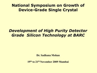
- 1. National Symposium on Growth of Device-Grade Single Crystal Development of High Purity Detector Grade Silicon Technology at BARC Dr. Sadhana Mohan 19th to 21th November 2009 Mumbai
- 2. 2 Outline of the presentation 1. Role of silicon in advanced technologies 2. Detector Grade Silicon 3. BARC Roadmap of silicon technology development 4. Detector Grade Silicon Production routes 5. Process Selection Criteria 6. Product characterization 7. Status of Detector Grade Silicon Production at BARC 8. Conclusion 20th Nov, 09 Dr. Sadhana Mohan, BARC, Mumbai
- 3. 3 We have entered the age of super computing , multimedia and instant communication. In today’ s scenario, life is unimaginable without these gadgets Silicon is the foundation of these sophisticated and advanced technologies . Over 80% of semiconductor industry base is crystalline silicon, out of which 5% is the share of detector grade As on today ,photovoltaic grade silicon production technology is commercially available while detector grade technology is still closely guarded 20th Nov, 09 Dr. Sadhana Mohan, BARC, Mumbai Role of silicon in advanced technologies
- 4. 4 Why silicon in general has major share ? 20th Nov, 09 Dr. Sadhana Mohan, BARC, Mumbai Silicon is most fascinating semiconductor material due to its favorable energy gap, insulating properties and the ease with which its electronic properties can be altered. It is the second largest element after oxygen in the earth crust It has better thermo physical properties which determine how heat and mass transport can be managed at the time of crystal growth silicon has reasonably high thermal conductivity, stacking fault energy and critical resolved shear stress conforming its ability to make large size dislocation free single crystal.
- 5. 5 Silicon MEMS IC ULSI/VLSI Solar Cell Silicon Mirror Porous silicon Radiation Detector High Power Devices IR Reflectors & Windows Overall spectrum of silicon applications 19th Nov, 09 NSRC, Mumbai
- 6. Applications of High Purity Silicon Purity of Silicon as determined by concentration of defects determines its suitability for applications. High Purity Silicon is used in microelectronics industry and in manufacturing of radiation detectors. Solar Grade (Cd≈10-6, 5 Ω-cm, 10 µsec) Microelectronic Grade (Cd≈10-6, 1KΩ-cm, 100 µsec) Detector Grade (Cd≈10-6, 30 KΩ-cm, 1000 µsec)
- 7. 7 Why do we need Detector grade silicon ? 20th Nov, 09 Dr. Sadhana Mohan, BARC, Mumbai To improve Large size integrated circuits (VLSI/ULSI) efficiency high resistivity defect free single crystal is the parent material To improve sensitivity of radiation detectors for detecting small quantities of high energy neutrons and charged particles needs negligible leakage current and large sensitive volume . Economic production of high power devices and high sensitivity radiation detectors demands large diameter detector grade single crystal ingot production facility .
- 8. 8 PREPARATION OF HR SINGLE CRYSTAL SILICON INGOT Metallurgical grade silicon CO Si C SiO 2 2 2 TCS Production 2 3 3 H SiHCl HCl Si TCS Purification TCS purification by distillation Si: 98% Polysilicon Production in a CVD reactor HCl Si H SiHCl 3 2 3 Si: 99.999999999% HR Single crystal silicon ingot production in a FZ crystal puller
- 9. 9 Front End facility development Backend Facility development Poly silicon production BARC Parallel approach to technology development UHP grade TCS purification TCS production Float Zone Crystal pulling Wafer production Wafer Characterization Detector Fabrication Central Crystal Pulling Facility 20th Nov, 09 Dr. Sadhana Mohan, BARC, Mumbai Neutron Transmutation Single Crystal Pulling Facility Detector Testing
- 10. 10 Major Commercially viable Technology options 20th Nov, 09 • Siemens process • Trichlorosilane as volatile precursor • Most preferred process as 80% of commercial market is captured by Siemens process • Major :Wacker chemie, Hemlock, • Union carbide process • Silane as volatile precursor • ASIMI taken over union carbide and komatsu Front End Facility Development
- 11. 11 Union carbide process 20th Nov, 09 Dr. Sadhana Mohan, BARC, Mumbai • Distinct advantages • Better purification due to large separation factors for major impurities • Non corrosive system • Less recycled product handling at poly step • Major issues • Difficult to manufacture with low yield and large recycle • Handling of Non target deposition at poly step • Gas at room temperature high pressure storage • Pyrophoric in nature Front End Facility Development Mg-Si Intermediate SiH4 HR Silicon UNION CARBIDE PROECSS
- 12. 12 Siemens process 20th Nov, 09 Dr. Sadhana Mohan, BARC, Mumbai Distinct advantages • Less number of process steps • Better overall production yield • Liquid at room temperature • Non pyrophoric Major issues: • Highly corrosive in presence of moisture • Hardens most of the sealing materials • Clogs small sample tubes if left open after use • Needs proper ventilated secondary containment Front End Facility Development Mg-Si Intermediate SiHCl3 HR Silicon SIEMENS PROECSS
- 13. 13 TCS production 20th Nov, 09 Dr. Sadhana Mohan, BARC, Mumbai Properties of TCS: Boiling Point: 32 oC Flammability Range: 7 to 86% DOT Class: 4.3 (dangerous when wet) TLV: 5 ppm STEL: 100 ppm Heat of Combustion: 494 kJ/mol Flash Point: -17 oC Auto Ignition Point: 170 oC Front End Facility Development Mg-Si HCl (g) TCS (g) + STC(g) + H2 (g) +HCl (g) Condenser H2 (g) +HCl (g) TCS (l) + STC(l) FBR
- 14. 14 TCS purification 20th Nov, 09 Dr. Sadhana Mohan, BARC, Mumbai Design intent High integrity helium leak tested joints highly electropolished SS surface, ppt level purification in five stage squared off distillation cascade, enough redundancy Key issues ppt level analysis Sustained operation of Boiling TCS handling pump Arresting TCS leak in case of abnormalities Handling clogging in case of improper purging Front End Facility Development
- 15. 15 Polysilicon production 20th Nov, 09 Dr. Sadhana Mohan, BARC, Mumbai Cold wall CVD reactor Specific advantages :No scale up issues ,No joining issues to base plate and reactor wall, No operating pressure limit Preferred in Photovoltaic grade silicon production Quartz CVD reactors Specific advantage Better purity of poly produced preferred for detector grade Front End Facility Development
- 16. 16 Influence of operating parameters 20th Nov, 09 Dr. Sadhana Mohan, BARC, Mumbai Simulation Results : Increasing pressure decreases Equillibrium yield but increases rate of production Increasing TCS to Hydrogen ration decreses equillibrium yield but increases production Yield increases substantially upto 1100c At low scale low pressure low TCS is better while at large scale it is higher pressure higher TCS concentration is preferred one Specific issues: Temperature contol of growing surface Deposition control with time acrobolite formation of quartz making it opaque Preheating of near insulating slim rod at room temperatureCore meltdown in case of improper heat transfer Front End Facility Development
- 17. 17 Large size Single crystal pulling 20th Nov, 09 Dr. Sadhana Mohan, BARC, Mumbai Cz process photo its distinct advantages Gravity stablised molten zone Less operators control less steep temperature gradient Central crystal pulling facility
- 18. 18 Large size Single crystal pulling 20th Nov, 09 Dr. Sadhana Mohan, BARC, Mumbai Cz process photo its distinct advantages Gravity stablised molten zone Less operators control less steep temperature gradient Crystal seed Molten polysilic on Heat shield Water jacket Single crystal silicon Quartz crucible Carbon heating element Crystal puller and rotation mechanism
- 19. 19 Float zone crystal pulling 20th Nov, 09 Dr. Sadhana Mohan, BARC, Mumbai Distinct advantages No containment impurity pickup by molten silicon Less power requirement due to small molten zone Less silicon inventory loss No problem of crucible cracking due to volume expansion after solidification Most Suited for Large size defect free crystal detector grade silicon Key issues Floating molten zone instability Vibration control Arching control Argon purity control Class 10 environment control Proper Engagement of support system for large weight support system less steep temperature gradient Our observations: Central crystal pulling facility
- 20. 20 Float zone crystal pulling 20th Nov, 09 Dr. Sadhana Mohan, BARC, Mumbai Distinct advantages • No containment impurity pickup by molten silicon • Less power requirement due to small molten zone • Less silicon inventory loss • No problem of crucible cracking due to volume expansion after solidification • Most Suited for Large size defect free crystal detector grade silicon Central crystal pulling facility
- 21. 21 Float zone crystal pulling 20th Nov, 09 Dr. Sadhana Mohan, BARC, Mumbai Key issues • Floating molten zone instability • Vibration control • Arching control • Argon purity control • Class 10 environment control • Proper Engagement of support system for large weight support system • less steep temperature gradient Our observations: Central crystal pulling facility
- 22. 22 FZ machine for single crystal silicon production
- 23. 23 Complexities involved in Silicon crystal pulling 20th Nov, 09 Dr. Sadhana Mohan, BARC, Mumbai Maintenance of Steady & Uninterrupted Power Supply to the Reactor for Very Long Time (continuously 15 days) Very Fine & Vibration free Control of Moving and Rotating parts Arching Problem during Crystal Pulling Very Fine Control of Power Input is Required because of Solidification or Spillage problem Minimization of Crystal Structural Defects Making Long Single Crystal (1000 mm) Mechanical Fabrication (Turning, Grinding etc.) Difficulties of 1000 mm long and 100 mm dia. Rods Providing Cooling to Coil and other Structural parts Central crystal pulling facility
- 24. 24 Wafer preparation: Slicing 20th Nov, 09 Dr. Sadhana Mohan, BARC, Mumbai Central crystal pulling facility Single Crystal silicon ingot End Cutting OD Grinding Flat Grinding Wafer Slicing Wafer Polishing Wafer Lapping Edge Rounding PRIME GRADE Si WAFER
- 25. Cropping is the first step for preparing the crystal for wafering. In this step end conical portions of ingot is sliced off. Purpose: – to cut the crystal to a suitable length to fit the saw capacity. – to obtain samples for oxygen and carbon measurements. – to select portions of the crystal which meet desired resistivity specification. Wafer preparation: Cropping Important Aspects – Commercial cropping equipment ranges from simple hand-operated cut-off machines to those which hydraulically clamp the crystal and move the blade through the crystal – The blade diameter must be sufficiently large to cut completely through the crystal in one pass in order to obtain a smooth and straight cut. – ID saw machine is mostly preferred to minimize kerf loss and material damage and for smooth cutting.
- 26. OD Grinding: Crystal outer diameter is ground to the required diameter using a fixed abrasive grinding wheel. Purpose: • to obtain wafers of precise diameter. Issues • Improper grinding may create problem of exit chipping in wafering and lattice slip in thermal processing. Wafer preparation: OD Grinding Center less Grinding Grinding on Centers
- 27. Wafer preparation: Flat Grinding Flat Grinding: Silicon crystals are grown with either the crystallographic <loo> or <111> direction parallel to the cylindrical axis of the crystal. The identification flats (there may be one or two on a crystal) are ground lengthwise along the crystal according the to the crystal orientation and the dopant type. The largest flat is called the primary flat, and is used for positioning the wafer for front end processing such as patterning or dicing. A secondary flat may also be ground on the crystal. The specific arrangements of flats make it easy to identify the orientation (111 or 100) and the material (n- or p-type). SEMI locations for orientation/identification flats
- 28. Wafer preparation: Wafer slicing 28 Inner Diameter Sawing Imbedded diamond particles 350-400 μm (kerf loss) wafer ID saw blade (rotating) Material properties: Silicon is a very hard and brittle material (Mohs’ hardness scale: 7-8 ) Diamond coated blades used for wafer slicing Specification of the final prepared wafers: Wafer thickness: 300-1000 µm TTV: <10 µm Kerf loss: < 0.4 mm Bow: < 30 µm Surface damage: <2 µm Preparation of work piece for mounting ingot Work piece guide (graphite) Adhesive
- 29. 29 Wafer preparation: Slicing 20th Nov, 09 Dr. Sadhana Mohan, BARC, Mumbai Central crystal pulling facility Wafer Slicing: Wafer slicing from silicon block are mainly performed by ID saw machine
- 30. 30 Associated Semiconductor Industry 20th Nov, 09 Dr. Sadhana Mohan, BARC, Mumbai Central crystal pulling facility
- 31. 31 Associated Semiconductor Industry 20th Nov, 09 Dr. Sadhana Mohan, BARC, Mumbai Central crystal pulling facility
- 32. 32 Wafer Characterisation 20th Nov, 09 Dr. Sadhana Mohan, BARC, Mumbai Front End Facility Development
- 33. 33 Wafer Characterisation 20th Nov, 09 Dr. Sadhana Mohan, BARC, Mumbai Front End Facility Development
- 34. 34 Neutron transmutation 20th Nov, 09 Dr. Sadhana Mohan, BARC, Mumbai Back End Facility Development
- 35. 35 Neutron transmutation 20th Nov, 09 Dr. Sadhana Mohan, BARC, Mumbai Back End Facility Development
- 36. 36 2002 2004 2006 2008 2010 2012 2014 2016 TCS Production Demonstration Process Selection Cleanroom Facility Demonstration Silicon mono Crystal Ingot Demonstration Poly Silicon Ingot Production 2009 BARC Silicon Wafer Production Technology Road-map Major Milestone TCS Purification Integrated Technology Demonstration Wafer Production 20th Nov, 09 Dr. Sadhana Mohan, BARC, Mumbai