Download to read offline
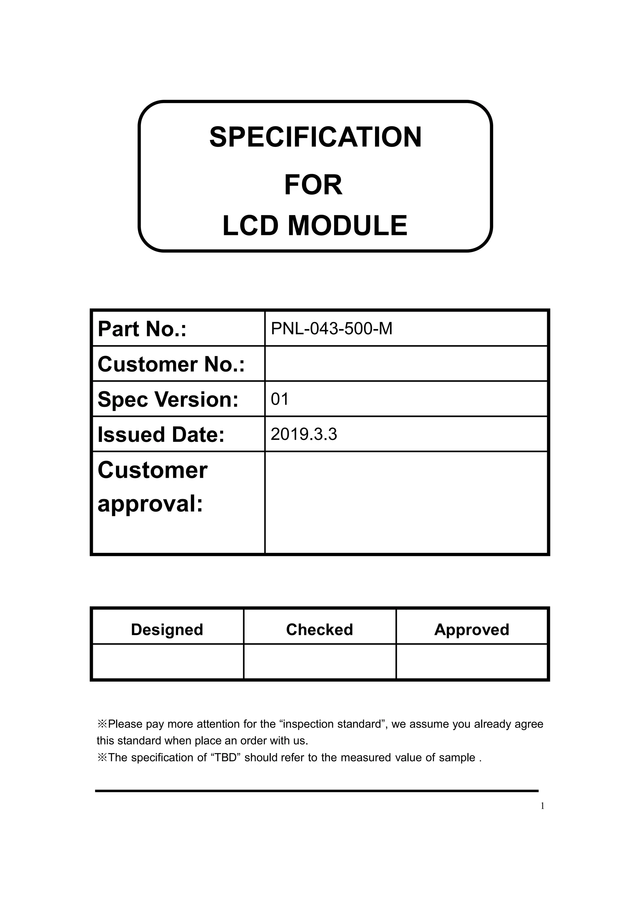


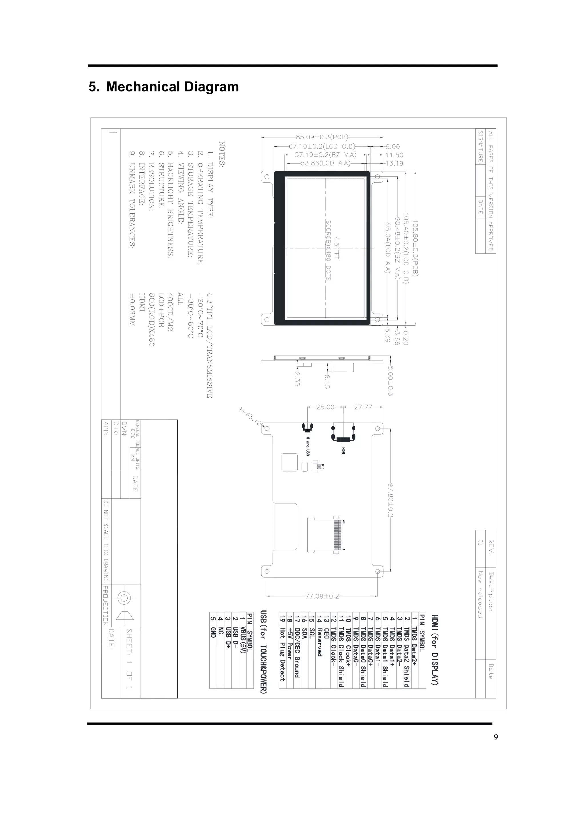


The document provides specifications for the PNL-043-500-M, a 4.3" IPS TFT LCD module with HDMI interface and a resolution of 800x480 pixels. It details mechanical, electrical, optical characteristics, inspection standards, and handling precautions for the display module. Additionally, it outlines customer approval requirements and emphasizes the importance of adhering to specified operating conditions to ensure optimal performance.


![Vibe Coding vs. Spec-Driven Development [Free Meetup]](https://cdn.slidesharecdn.com/ss_thumbnails/vibecodingvsspecdrivendevelopment-251209105622-43f455e7-thumbnail.jpg?width=640&height=640&fit=bounds)


