1. 1
Benzocyclobutene-Based Intracortical Neural Recording Probes
Charles Carter1, Haixin Zhu2, Jiping He1
1 Arizona State University, Department of Bioengineering, Tempe, AZ 85287
2 Arizona State University, Department of Electrical Engineering, Tempe, AZ 85287
For years, scientists have been using electrodes to
record electrical signals from the central and
peripheral nervous systems of living organisms.
(Schmidt, Bak and McIntosh, 1976) In more recent
times, this type of neuronal recording has found
application in medical therapies designed to restore
limited mobility or a means of communication to
tetrapalegics.(Kennedy et al., 2000) While this type
of brain-machine interface holds promise for a
variety of additional medical applications, the
recording electrodes utilized in this neural interface
design inevitably lose their functionality after long
periods of time in vivo. Two reasons for this include
the harshness of the biological environment as well
as implant isolation due to the organism’s foreign
body response.(Edell et al., 1992) In recent times,
researchers have applied microfabrication techniques
to the development of sophisticated recording arrays
designed to overcome the biocompatibility challenges
associated with their precursors. These arrays can be
designed to enhance biocompatability by being
flexible as well as by incorporating wells to be
seeded with bioactive agents.(Rousche et al., 2001)
In addition, these new arrays may obtain better signal
integrity by incorporating on-chip signal processing
elements. Such features may allow this new
generation of electrodes to obtain higher quality
neuronal recordings for long periods of time. Our
research focuses on the development of one such
next-generation flexible neuronal recording device
utilizing 3022-63 Benzocyclobutene (BCB) as the
insulating material.
We are currently in the stages of refining the
fabrication process for our neuronal recording probe
in order to make it more robust. The process begins
with a standard silicon wafer coated with 5000Å
thermal oxide. The wafer is spin coated with 20µm
3022 BCB resin which is then partially cured in an
inert atmosphere at 210°C for 40 minutes. A metal
evaporator is then used to sequentially deposit 200 Å
Cr, 2000 Å Au, and 200 Å Cr. Photolithography is
then used to pattern electrical traces on the polymer.
A second layer of BCB resin is then deposited 10µm
thick and partially cured at 210°C for 40 minutes.
3000 Å of Al is then electron beam evaporated onto
the surface, patterned and etched as a protective mask
for reactive ion etch. The sample is then exposed to
reactive ion etch (5sccm CF4, 20sccm O2) for 25
minutes. The aluminum mask is then patterned and
etched again to expose the BCB covering the 20 µm
by 20 µm neural recording sites as well as the
connectors of the device. The sample is then etched
for another 15 minutes in reactive ion etch. The
aluminum hard mask is then removed and the sample
is fully cured at 250°C for 60 minutes. The device is
then removed from the substrate with a 49%
hydrofluoric acid solution.
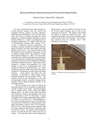
Figure 1: BCB-based neural recording array on the face of
a penny.