
Recommended
More Related Content
Similar to pic16f877.pdf
Similar to pic16f877.pdf (20)
More from Aarthi Venkatesh N
Recently uploaded
Recently uploaded (20)
pic16f877.pdf
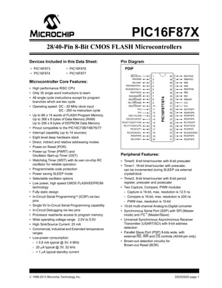
- 1. 1998-2013 Microchip Technology Inc. DS30292D-page 1 PIC16F87X Devices Included in this Data Sheet: Microcontroller Core Features: • High performance RISC CPU • Only 35 single word instructions to learn • All single cycle instructions except for program branches which are two cycle • Operating speed: DC - 20 MHz clock input DC - 200 ns instruction cycle • Up to 8K x 14 words of FLASH Program Memory, Up to 368 x 8 bytes of Data Memory (RAM) Up to 256 x 8 bytes of EEPROM Data Memory • Pinout compatible to the PIC16C73B/74B/76/77 • Interrupt capability (up to 14 sources) • Eight level deep hardware stack • Direct, indirect and relative addressing modes • Power-on Reset (POR) • Power-up Timer (PWRT) and Oscillator Start-up Timer (OST) • Watchdog Timer (WDT) with its own on-chip RC oscillator for reliable operation • Programmable code protection • Power saving SLEEP mode • Selectable oscillator options • Low power, high speed CMOS FLASH/EEPROM technology • Fully static design • In-Circuit Serial Programming(ICSP)via two pins • Single 5V In-Circuit Serial Programming capability • In-Circuit Debugging via two pins • Processor read/write access to program memory • Wide operating voltage range: 2.0V to 5.5V • High Sink/Source Current: 25 mA • Commercial, Industrial and Extended temperature ranges • Low-power consumption: - < 0.6 mA typical @ 3V, 4 MHz - 20 A typical @ 3V, 32 kHz - < 1 A typical standby current Pin Diagram Peripheral Features: • Timer0: 8-bit timer/counter with 8-bit prescaler • Timer1: 16-bit timer/counter with prescaler, can be incremented during SLEEP via external crystal/clock • Timer2: 8-bit timer/counter with 8-bit period register, prescaler and postscaler • Two Capture, Compare, PWM modules - Capture is 16-bit, max. resolution is 12.5 ns - Compare is 16-bit, max. resolution is 200 ns - PWM max. resolution is 10-bit • 10-bit multi-channel Analog-to-Digital converter • Synchronous Serial Port (SSP) with SPI (Master mode) and I2 C (Master/Slave) • Universal Synchronous Asynchronous Receiver Transmitter (USART/SCI) with 9-bit address detection • Parallel Slave Port (PSP) 8-bits wide, with external RD, WR and CS controls (40/44-pin only) • Brown-out detection circuitry for Brown-out Reset (BOR) • PIC16F873 • PIC16F874 • PIC16F876 • PIC16F877 RB7/PGD RB6/PGC RB5 RB4 RB3/PGM RB2 RB1 RB0/INT VDD VSS RD7/PSP7 RD6/PSP6 RD5/PSP5 RD4/PSP4 RC7/RX/DT RC6/TX/CK RC5/SDO RC4/SDI/SDA RD3/PSP3 RD2/PSP2 MCLR/VPP RA0/AN0 RA1/AN1 RA2/AN2/VREF- RA3/AN3/VREF+ RA4/T0CKI RA5/AN4/SS RE0/RD/AN5 RE1/WR/AN6 RE2/CS/AN7 VDD VSS OSC1/CLKIN OSC2/CLKOUT RC0/T1OSO/T1CKI RC1/T1OSI/CCP2 RC2/CCP1 RC3/SCK/SCL RD0/PSP0 RD1/PSP1 1 2 3 4 5 6 7 8 9 10 11 12 13 14 15 16 17 18 19 20 40 39 38 37 36 35 34 33 32 31 30 29 28 27 26 25 24 23 22 21 PIC16F877/874 PDIP 28/40-Pin 8-Bit CMOS FLASH Microcontrollers
- 2. PIC16F87X DS30292D-page 2 1998-2013 Microchip Technology Inc. Pin Diagrams PIC16F876/873 10 11 2 3 4 5 6 1 8 7 9 12 13 14 15 16 17 18 19 20 23 24 25 26 27 28 22 21 MCLR/VPP RA0/AN0 RA1/AN1 RA2/AN2/VREF- RA3/AN3/VREF+ RA4/T0CKI RA5/AN4/SS VSS OSC1/CLKIN OSC2/CLKOUT RC0/T1OSO/T1CKI RC1/T1OSI/CCP2 RC2/CCP1 RC3/SCK/SCL RB7/PGD RB6/PGC RB5 RB4 RB3/PGM RB2 RB1 RB0/INT VDD VSS RC7/RX/DT RC6/TX/CK RC5/SDO RC4/SDI/SDA 10 11 12 13 14 15 16 17 18 19 20 21 22 23 24 25 26 44 8 7 6 5 4 3 2 1 27 282 9 30 31 32 33 34 35 36 37 38 39 40 41 42 43 9 PIC16F877 RA4/T0CKI RA5/AN4/SS RE0/RD/AN5 OSC1/CLKIN OSC2/CLKOUT RC0/T1OSO/T1CK1 NC RE1/WR/AN6 RE2/CS/AN7 VDD VSS RB3/PGM RB2 RB1 RB0/INT VDD VSS RD7/PSP7 RD6/PSP6 RD5/PSP5 RD4/PSP4 RC7/RX/DT RA3/AN3/V REF + RA2/AN2/V REF - RA1/AN1 RA0/AN0 MCLR/V PP NC RB7/PGD RB6/PGC RB5 RB4 NC NC RC6/TX/CK RC5/SDO RC4/SDI/SDA RD3/PSP3 RD2/PSP2 RD1/PSP1 RD0/PSP0 RC3/SCK/SCL RC2/CCP1 RC1/T1OSI/CCP2 10 11 2 3 4 5 6 1 18 19 20 21 22 12 13 14 15 38 8 7 44 43 42 41 40 39 16 17 29 30 31 32 33 23 24 25 26 27 28 36 34 35 9 PIC16F877 37 RA3/AN3/V REF + RA2/AN2/V REF - RA1/AN1 RA0/AN0 MCLR/V PP NC RB7/PGD RB6/PGC RB5 RB4 NC RC6/TX/CK RC5/SDO RC4/SDI/SDA RD3/PSP3 RD2/PSP2 RD1/PSP1 RD0/PSP0 RC3/SCK/SCL RC2/CCP1 RC1/T1OSI/CCP2 NC NC RC0/T1OSO/T1CKI OSC2/CLKOUT OSC1/CLKIN VSS VDD RE2/AN7/CS RE1/AN6/WR RE0/AN5/RD RA5/AN4/SS RA4/T0CKI RC7/RX/DT RD4/PSP4 RD5/PSP5 RD6/PSP6 RD7/PSP7 VSS VDD RB0/INT RB1 RB2 RB3/PGM PLCC QFP PDIP, SOIC PIC16F874 PIC16F874
- 3. 1998-2013 Microchip Technology Inc. DS30292D-page 3 PIC16F87X Key Features PIC® MCU Mid-Range Reference Manual (DS33023) PIC16F873 PIC16F874 PIC16F876 PIC16F877 Operating Frequency DC - 20 MHz DC - 20 MHz DC - 20 MHz DC - 20 MHz RESETS (and Delays) POR, BOR (PWRT, OST) POR, BOR (PWRT, OST) POR, BOR (PWRT, OST) POR, BOR (PWRT, OST) FLASH Program Memory (14-bit words) 4K 4K 8K 8K Data Memory (bytes) 192 192 368 368 EEPROM Data Memory 128 128 256 256 Interrupts 13 14 13 14 I/O Ports Ports A,B,C Ports A,B,C,D,E Ports A,B,C Ports A,B,C,D,E Timers 3 3 3 3 Capture/Compare/PWM Modules 2 2 2 2 Serial Communications MSSP, USART MSSP, USART MSSP, USART MSSP, USART Parallel Communications — PSP — PSP 10-bit Analog-to-Digital Module 5 input channels 8 input channels 5 input channels 8 input channels Instruction Set 35 instructions 35 instructions 35 instructions 35 instructions
- 4. PIC16F87X DS30292D-page 4 1998-2013 Microchip Technology Inc. Table of Contents 1.0 Device Overview ................................................................................................................................................... 5 2.0 Memory Organization.......................................................................................................................................... 11 3.0 I/O Ports.............................................................................................................................................................. 29 4.0 Data EEPROM and FLASH Program Memory.................................................................................................... 41 5.0 Timer0 Module .................................................................................................................................................... 47 6.0 Timer1 Module .................................................................................................................................................... 51 7.0 Timer2 Module .................................................................................................................................................... 55 8.0 Capture/Compare/PWM Modules ....................................................................................................................... 57 9.0 Master Synchronous Serial Port (MSSP) Module............................................................................................... 65 10.0 Addressable Universal Synchronous Asynchronous Receiver Transmitter (USART) ........................................ 95 11.0 Analog-to-Digital Converter (A/D) Module......................................................................................................... 111 12.0 Special Features of the CPU............................................................................................................................. 119 13.0 Instruction Set Summary................................................................................................................................... 135 14.0 Development Support ....................................................................................................................................... 143 15.0 Electrical Characteristics................................................................................................................................... 149 16.0 DC and AC Characteristics Graphs and Tables................................................................................................ 177 17.0 Packaging Information ...................................................................................................................................... 189 Appendix A: Revision History .................................................................................................................................... 197 Appendix B: Device Differences ................................................................................................................................ 197 Appendix C: Conversion Considerations ................................................................................................................... 198 Index .......................................................................................................................................................................... 199 On-Line Support......................................................................................................................................................... 207 Reader Response ...................................................................................................................................................... 208 PIC16F87X Product Identification System ................................................................................................................. 209 TO OUR VALUED CUSTOMERS It is our intention to provide our valued customers with the best documentation possible to ensure successful use of your Microchip products. To this end, we will continue to improve our publications to better suit your needs. Our publications will be refined and enhanced as new volumes and updates are introduced. If you have any questions or comments regarding this publication, please contact the Marketing Communications Department via E-mail at docerrors@mail.microchip.com or fax the Reader Response Form in the back of this data sheet to (480) 792-4150. We welcome your feedback. Most Current Data Sheet To obtain the most up-to-date version of this data sheet, please register at our Worldwide Web site at: http://www.microchip.com You can determine the version of a data sheet by examining its literature number found on the bottom outside corner of any page. The last character of the literature number is the version number, (e.g., DS30000A is version A of document DS30000). Errata An errata sheet, describing minor operational differences from the data sheet and recommended workarounds, may exist for current devices. As device/documentation issues become known to us, we will publish an errata sheet. The errata will specify the revision of silicon and revision of document to which it applies. To determine if an errata sheet exists for a particular device, please check with one of the following: • Microchip’s Worldwide Web site; http://www.microchip.com • Your local Microchip sales office (see last page) • The Microchip Corporate Literature Center; U.S. FAX: (480) 792-7277 When contacting a sales office or the literature center, please specify which device, revision of silicon and data sheet (include liter- ature number) you are using. Customer Notification System Register on our web site at www.microchip.com/cn to receive the most current information on all of our products.
- 5. 1998-2013 Microchip Technology Inc. DS30292D-page 5 PIC16F87X 1.0 DEVICE OVERVIEW This document contains device specific information. Additional information may be found in the PIC® MCU Mid-Range Reference Manual (DS33023), which may be obtained from your local Microchip Sales Represen- tative or downloaded from the Microchip website. The Reference Manual should be considered a complemen- tary document to this data sheet, and is highly recom- mended reading for a better understanding of the device architecture and operation of the peripheral modules. There are four devices (PIC16F873, PIC16F874, PIC16F876 and PIC16F877) covered by this data sheet. The PIC16F876/873 devices come in 28-pin packages and the PIC16F877/874 devices come in 40-pin packages. The Parallel Slave Port is not implemented on the 28-pin devices. The following device block diagrams are sorted by pin number; 28-pin for Figure 1-1 and 40-pin for Figure 1-2. The 28-pin and 40-pin pinouts are listed in Table 1-1 and Table 1-2, respectively. FIGURE 1-1: PIC16F873 AND PIC16F876 BLOCK DIAGRAM FLASH Program Memory 13 Data Bus 8 14 Program Bus Instruction reg Program Counter 8 Level Stack (13-bit) RAM File Registers Direct Addr 7 RAM Addr(1) 9 Addr MUX Indirect Addr FSR reg STATUS reg MUX ALU W reg Power-up Timer Oscillator Start-up Timer Power-on Reset Watchdog Timer Instruction Decode & Control Timing Generation OSC1/CLKIN OSC2/CLKOUT MCLR VDD, VSS PORTA PORTB PORTC RA4/T0CKI RA5/AN4/SS RB0/INT RC0/T1OSO/T1CKI RC1/T1OSI/CCP2 RC2/CCP1 RC3/SCK/SCL RC4/SDI/SDA RC5/SDO RC6/TX/CK RC7/RX/DT 8 8 Brown-out Reset Note 1: Higher order bits are from the STATUS register. USART CCP1,2 Synchronous 10-bit A/D Timer0 Timer1 Timer2 Serial Port RA3/AN3/VREF+ RA2/AN2/VREF- RA1/AN1 RA0/AN0 8 3 Data EEPROM RB1 RB2 RB3/PGM RB4 RB5 RB6/PGC RB7/PGD Device Program FLASH Data Memory Data EEPROM PIC16F873 4K 192 Bytes 128 Bytes PIC16F876 8K 368 Bytes 256 Bytes In-Circuit Debugger Low Voltage Programming
- 6. PIC16F87X DS30292D-page 6 1998-2013 Microchip Technology Inc. FIGURE 1-2: PIC16F874 AND PIC16F877 BLOCK DIAGRAM FLASH Program Memory 13 Data Bus 8 14 Program Bus Instruction reg Program Counter 8 Level Stack (13-bit) RAM File Registers Direct Addr 7 RAM Addr(1) 9 Addr MUX Indirect Addr FSR reg STATUS reg MUX ALU W reg Power-up Timer Oscillator Start-up Timer Power-on Reset Watchdog Timer Instruction Decode & Control Timing Generation OSC1/CLKIN OSC2/CLKOUT MCLR VDD, VSS PORTA PORTB PORTC PORTD PORTE RA4/T0CKI RA5/AN4/SS RC0/T1OSO/T1CKI RC1/T1OSI/CCP2 RC2/CCP1 RC3/SCK/SCL RC4/SDI/SDA RC5/SDO RC6/TX/CK RC7/RX/DT RE0/AN5/RD RE1/AN6/WR RE2/AN7/CS 8 8 Brown-out Reset Note 1: Higher order bits are from the STATUS register. USART CCP1,2 Synchronous 10-bit A/D Timer0 Timer1 Timer2 Serial Port RA3/AN3/VREF+ RA2/AN2/VREF- RA1/AN1 RA0/AN0 Parallel Slave Port 8 3 Data EEPROM RB0/INT RB1 RB2 RB3/PGM RB4 RB5 RB6/PGC RB7/PGD Device Program FLASH Data Memory Data EEPROM PIC16F874 4K 192 Bytes 128 Bytes PIC16F877 8K 368 Bytes 256 Bytes In-Circuit Debugger Low-Voltage Programming RD0/PSP0 RD1/PSP1 RD2/PSP2 RD3/PSP3 RD4/PSP4 RD5/PSP5 RD6/PSP6 RD7/PSP7
- 7. 1998-2013 Microchip Technology Inc. DS30292D-page 7 PIC16F87X TABLE 1-1: PIC16F873 AND PIC16F876 PINOUT DESCRIPTION Pin Name DIP Pin# SOIC Pin# I/O/P Type Buffer Type Description OSC1/CLKIN 9 9 I ST/CMOS(3) Oscillator crystal input/external clock source input. OSC2/CLKOUT 10 10 O — Oscillator crystal output. Connects to crystal or resonator in crystal oscillator mode. In RC mode, the OSC2 pin outputs CLKOUT which has 1/4 the frequency of OSC1, and denotes the instruction cycle rate. MCLR/VPP 1 1 I/P ST Master Clear (Reset) input or programming voltage input. This pin is an active low RESET to the device. PORTA is a bi-directional I/O port. RA0/AN0 2 2 I/O TTL RA0 can also be analog input0. RA1/AN1 3 3 I/O TTL RA1 can also be analog input1. RA2/AN2/VREF- 4 4 I/O TTL RA2 can also be analog input2 or negative analog reference voltage. RA3/AN3/VREF+ 5 5 I/O TTL RA3 can also be analog input3 or positive analog reference voltage. RA4/T0CKI 6 6 I/O ST RA4 can also be the clock input to the Timer0 module. Output is open drain type. RA5/SS/AN4 7 7 I/O TTL RA5 can also be analog input4 or the slave select for the synchronous serial port. PORTB is a bi-directional I/O port. PORTB can be software programmed for internal weak pull-up on all inputs. RB0/INT 21 21 I/O TTL/ST(1) RB0 can also be the external interrupt pin. RB1 22 22 I/O TTL RB2 23 23 I/O TTL RB3/PGM 24 24 I/O TTL RB3 can also be the low voltage programming input. RB4 25 25 I/O TTL Interrupt-on-change pin. RB5 26 26 I/O TTL Interrupt-on-change pin. RB6/PGC 27 27 I/O TTL/ST(2) Interrupt-on-change pin or In-Circuit Debugger pin. Serial programming clock. RB7/PGD 28 28 I/O TTL/ST(2) Interrupt-on-change pin or In-Circuit Debugger pin. Serial programming data. PORTC is a bi-directional I/O port. RC0/T1OSO/T1CKI 11 11 I/O ST RC0 can also be the Timer1 oscillator output or Timer1 clock input. RC1/T1OSI/CCP2 12 12 I/O ST RC1 can also be the Timer1 oscillator input or Capture2 input/Compare2 output/PWM2 output. RC2/CCP1 13 13 I/O ST RC2 can also be the Capture1 input/Compare1 output/ PWM1 output. RC3/SCK/SCL 14 14 I/O ST RC3 can also be the synchronous serial clock input/output for both SPI and I2 C modes. RC4/SDI/SDA 15 15 I/O ST RC4 can also be the SPI Data In (SPI mode) or data I/O (I2C mode). RC5/SDO 16 16 I/O ST RC5 can also be the SPI Data Out (SPI mode). RC6/TX/CK 17 17 I/O ST RC6 can also be the USART Asynchronous Transmit or Synchronous Clock. RC7/RX/DT 18 18 I/O ST RC7 can also be the USART Asynchronous Receive or Synchronous Data. VSS 8, 19 8, 19 P — Ground reference for logic and I/O pins. VDD 20 20 P — Positive supply for logic and I/O pins. Legend: I = input O = output I/O = input/output P = power — = Not used TTL = TTL input ST = Schmitt Trigger input Note 1: This buffer is a Schmitt Trigger input when configured as the external interrupt. 2: This buffer is a Schmitt Trigger input when used in Serial Programming mode. 3: This buffer is a Schmitt Trigger input when configured in RC oscillator mode and a CMOS input otherwise.
- 8. PIC16F87X DS30292D-page 8 1998-2013 Microchip Technology Inc. TABLE 1-2: PIC16F874 AND PIC16F877 PINOUT DESCRIPTION Pin Name DIP Pin# PLCC Pin# QFP Pin# I/O/P Type Buffer Type Description OSC1/CLKIN 13 14 30 I ST/CMOS(4) Oscillator crystal input/external clock source input. OSC2/CLKOUT 14 15 31 O — Oscillator crystal output. Connects to crystal or resonator in crystal oscillator mode. In RC mode, OSC2 pin outputs CLKOUT which has 1/4 the frequency of OSC1, and denotes the instruction cycle rate. MCLR/VPP 1 2 18 I/P ST Master Clear (Reset) input or programming voltage input. This pin is an active low RESET to the device. PORTA is a bi-directional I/O port. RA0/AN0 2 3 19 I/O TTL RA0 can also be analog input0. RA1/AN1 3 4 20 I/O TTL RA1 can also be analog input1. RA2/AN2/VREF- 4 5 21 I/O TTL RA2 can also be analog input2 or negative analog reference voltage. RA3/AN3/VREF+ 5 6 22 I/O TTL RA3 can also be analog input3 or positive analog reference voltage. RA4/T0CKI 6 7 23 I/O ST RA4 can also be the clock input to the Timer0 timer/ counter. Output is open drain type. RA5/SS/AN4 7 8 24 I/O TTL RA5 can also be analog input4 or the slave select for the synchronous serial port. PORTB is a bi-directional I/O port. PORTB can be soft- ware programmed for internal weak pull-up on all inputs. RB0/INT 33 36 8 I/O TTL/ST(1) RB0 can also be the external interrupt pin. RB1 34 37 9 I/O TTL RB2 35 38 10 I/O TTL RB3/PGM 36 39 11 I/O TTL RB3 can also be the low voltage programming input. RB4 37 41 14 I/O TTL Interrupt-on-change pin. RB5 38 42 15 I/O TTL Interrupt-on-change pin. RB6/PGC 39 43 16 I/O TTL/ST(2) Interrupt-on-change pin or In-Circuit Debugger pin. Serial programming clock. RB7/PGD 40 44 17 I/O TTL/ST(2) Interrupt-on-change pin or In-Circuit Debugger pin. Serial programming data. Legend: I = input O = output I/O = input/output P = power — = Not used TTL = TTL input ST = Schmitt Trigger input Note 1: This buffer is a Schmitt Trigger input when configured as an external interrupt. 2: This buffer is a Schmitt Trigger input when used in Serial Programming mode. 3: This buffer is a Schmitt Trigger input when configured as general purpose I/O and a TTL input when used in the Parallel Slave Port mode (for interfacing to a microprocessor bus). 4: This buffer is a Schmitt Trigger input when configured in RC oscillator mode and a CMOS input otherwise.
- 9. 1998-2013 Microchip Technology Inc. DS30292D-page 9 PIC16F87X PORTC is a bi-directional I/O port. RC0/T1OSO/T1CKI 15 16 32 I/O ST RC0 can also be the Timer1 oscillator output or a Timer1 clock input. RC1/T1OSI/CCP2 16 18 35 I/O ST RC1 can also be the Timer1 oscillator input or Capture2 input/Compare2 output/PWM2 output. RC2/CCP1 17 19 36 I/O ST RC2 can also be the Capture1 input/Compare1 output/PWM1 output. RC3/SCK/SCL 18 20 37 I/O ST RC3 can also be the synchronous serial clock input/ output for both SPI and I2 C modes. RC4/SDI/SDA 23 25 42 I/O ST RC4 can also be the SPI Data In (SPI mode) or data I/O (I2 C mode). RC5/SDO 24 26 43 I/O ST RC5 can also be the SPI Data Out (SPI mode). RC6/TX/CK 25 27 44 I/O ST RC6 can also be the USART Asynchronous Transmit or Synchronous Clock. RC7/RX/DT 26 29 1 I/O ST RC7 can also be the USART Asynchronous Receive or Synchronous Data. PORTD is a bi-directional I/O port or parallel slave port when interfacing to a microprocessor bus. RD0/PSP0 19 21 38 I/O ST/TTL(3) RD1/PSP1 20 22 39 I/O ST/TTL(3) RD2/PSP2 21 23 40 I/O ST/TTL(3) RD3/PSP3 22 24 41 I/O ST/TTL(3) RD4/PSP4 27 30 2 I/O ST/TTL(3) RD5/PSP5 28 31 3 I/O ST/TTL(3) RD6/PSP6 29 32 4 I/O ST/TTL(3) RD7/PSP7 30 33 5 I/O ST/TTL(3) PORTE is a bi-directional I/O port. RE0/RD/AN5 8 9 25 I/O ST/TTL(3) RE0 can also be read control for the parallel slave port, or analog input5. RE1/WR/AN6 9 10 26 I/O ST/TTL(3) RE1 can also be write control for the parallel slave port, or analog input6. RE2/CS/AN7 10 11 27 I/O ST/TTL(3) RE2 can also be select control for the parallel slave port, or analog input7. VSS 12,31 13,34 6,29 P — Ground reference for logic and I/O pins. VDD 11,32 12,35 7,28 P — Positive supply for logic and I/O pins. NC — 1,17,28, 40 12,13, 33,34 — These pins are not internally connected. These pins should be left unconnected. TABLE 1-2: PIC16F874 AND PIC16F877 PINOUT DESCRIPTION (CONTINUED) Pin Name DIP Pin# PLCC Pin# QFP Pin# I/O/P Type Buffer Type Description Legend: I = input O = output I/O = input/output P = power — = Not used TTL = TTL input ST = Schmitt Trigger input Note 1: This buffer is a Schmitt Trigger input when configured as an external interrupt. 2: This buffer is a Schmitt Trigger input when used in Serial Programming mode. 3: This buffer is a Schmitt Trigger input when configured as general purpose I/O and a TTL input when used in the Parallel Slave Port mode (for interfacing to a microprocessor bus). 4: This buffer is a Schmitt Trigger input when configured in RC oscillator mode and a CMOS input otherwise.
- 10. PIC16F87X DS30292D-page 10 1998-2013 Microchip Technology Inc. NOTES:
- 11. 1998-2013 Microchip Technology Inc. DS30292D-page 11 PIC16F87X 2.0 MEMORY ORGANIZATION There are three memory blocks in each of the PIC16F87X MCUs. The Program Memory and Data Memory have separate buses so that concurrent access can occur and is detailed in this section. The EEPROM data memory block is detailed in Section 4.0. Additional information on device memory may be found in the PIC® MCU Mid-Range Reference Manual, (DS33023). FIGURE 2-1: PIC16F877/876 PROGRAM MEMORY MAP AND STACK 2.1 Program Memory Organization The PIC16F87X devices have a 13-bit program counter capable of addressing an 8K x 14 program memory space. The PIC16F877/876 devices have 8K x 14 words of FLASH program memory, and the PIC16F873/874 devices have 4K x 14. Accessing a location above the physically implemented address will cause a wraparound. The RESET vector is at 0000h and the interrupt vector is at 0004h. FIGURE 2-2: PIC16F874/873 PROGRAM MEMORY MAP AND STACK PC<12:0> 13 0000h 0004h 0005h Stack Level 1 Stack Level 8 RESET Vector Interrupt Vector On-Chip CALL, RETURN RETFIE, RETLW 1FFFh Stack Level 2 Program Memory Page 0 Page 1 Page 2 Page 3 07FFh 0800h 0FFFh 1000h 17FFh 1800h PC<12:0> 13 0000h 0004h 0005h Stack Level 1 Stack Level 8 RESET Vector Interrupt Vector On-Chip CALL, RETURN RETFIE, RETLW 1FFFh Stack Level 2 Program Memory Page 0 Page 1 07FFh 0800h 0FFFh 1000h
- 12. PIC16F87X DS30292D-page 12 1998-2013 Microchip Technology Inc. 2.2 Data Memory Organization The data memory is partitioned into multiple banks which contain the General Purpose Registers and the Special Function Registers. Bits RP1 (STATUS<6>) and RP0 (STATUS<5>) are the bank select bits. Each bank extends up to 7Fh (128 bytes). The lower locations of each bank are reserved for the Special Function Registers. Above the Special Function Regis- ters are General Purpose Registers, implemented as static RAM. All implemented banks contain Special Function Registers. Some frequently used Special Function Registers from one bank may be mirrored in another bank for code reduction and quicker access. 2.2.1 GENERAL PURPOSE REGISTER FILE The register file can be accessed either directly, or indi- rectly through the File Select Register (FSR). RP1:RP0 Bank 00 0 01 1 10 2 11 3 Note: EEPROM Data Memory description can be found in Section 4.0 of this data sheet.
- 13. 1998-2013 Microchip Technology Inc. DS30292D-page 13 PIC16F87X FIGURE 2-3: PIC16F877/876 REGISTER FILE MAP Indirect addr.(*) TMR0 PCL STATUS FSR PORTA PORTB PORTC PCLATH INTCON PIR1 TMR1L TMR1H T1CON TMR2 T2CON SSPBUF SSPCON CCPR1L CCPR1H CCP1CON OPTION_REG PCL STATUS FSR TRISA TRISB TRISC PCLATH INTCON PIE1 PCON PR2 SSPADD SSPSTAT 00h 01h 02h 03h 04h 05h 06h 07h 08h 09h 0Ah 0Bh 0Ch 0Dh 0Eh 0Fh 10h 11h 12h 13h 14h 15h 16h 17h 18h 19h 1Ah 1Bh 1Ch 1Dh 1Eh 1Fh 80h 81h 82h 83h 84h 85h 86h 87h 88h 89h 8Ah 8Bh 8Ch 8Dh 8Eh 8Fh 90h 91h 92h 93h 94h 95h 96h 97h 98h 99h 9Ah 9Bh 9Ch 9Dh 9Eh 9Fh 20h A0h 7Fh FFh Bank 0 Bank 1 Unimplemented data memory locations, read as '0'. * Not a physical register. Note 1: These registers are not implemented on the PIC16F876. 2: These registers are reserved, maintain these registers clear. File Address Indirect addr.(*) Indirect addr.(*) PCL STATUS FSR PCLATH INTCON PCL STATUS FSR PCLATH INTCON 100h 101h 102h 103h 104h 105h 106h 107h 108h 109h 10Ah 10Bh 10Ch 10Dh 10Eh 10Fh 110h 111h 112h 113h 114h 115h 116h 117h 118h 119h 11Ah 11Bh 11Ch 11Dh 11Eh 11Fh 180h 181h 182h 183h 184h 185h 186h 187h 188h 189h 18Ah 18Bh 18Ch 18Dh 18Eh 18Fh 190h 191h 192h 193h 194h 195h 196h 197h 198h 199h 19Ah 19Bh 19Ch 19Dh 19Eh 19Fh 120h 1A0h 17Fh 1FFh Bank 2 Bank 3 Indirect addr.(*) PORTD(1) PORTE(1) TRISD(1) ADRESL TRISE(1) TMR0 OPTION_REG PIR2 PIE2 RCSTA TXREG RCREG CCPR2L CCPR2H CCP2CON ADRESH ADCON0 TXSTA SPBRG ADCON1 General Purpose Register General Purpose Register General Purpose Register General Purpose Register 1EFh 1F0h accesses 70h - 7Fh EFh F0h accesses 70h-7Fh 16Fh 170h accesses 70h-7Fh General Purpose Register General Purpose Register TRISB PORTB 96 Bytes 80 Bytes 80 Bytes 80 Bytes 16 Bytes 16 Bytes SSPCON2 EEDATA EEADR EECON1 EECON2 EEDATH EEADRH Reserved(2) Reserved(2) File Address File Address File Address File Address
- 14. PIC16F87X DS30292D-page 14 1998-2013 Microchip Technology Inc. FIGURE 2-4: PIC16F874/873 REGISTER FILE MAP Indirect addr.(*) TMR0 PCL STATUS FSR PORTA PORTB PORTC PCLATH INTCON PIR1 TMR1L TMR1H T1CON TMR2 T2CON SSPBUF SSPCON CCPR1L CCPR1H CCP1CON OPTION_REG PCL STATUS FSR TRISA TRISB TRISC PCLATH INTCON PIE1 PCON PR2 SSPADD SSPSTAT 00h 01h 02h 03h 04h 05h 06h 07h 08h 09h 0Ah 0Bh 0Ch 0Dh 0Eh 0Fh 10h 11h 12h 13h 14h 15h 16h 17h 18h 19h 1Ah 1Bh 1Ch 1Dh 1Eh 1Fh 80h 81h 82h 83h 84h 85h 86h 87h 88h 89h 8Ah 8Bh 8Ch 8Dh 8Eh 8Fh 90h 91h 92h 93h 94h 95h 96h 97h 98h 99h 9Ah 9Bh 9Ch 9Dh 9Eh 9Fh 20h A0h 7Fh FFh Bank 0 Bank 1 Indirect addr.(*) Indirect addr.(*) PCL STATUS FSR PCLATH INTCON PCL STATUS FSR PCLATH INTCON 100h 101h 102h 103h 104h 105h 106h 107h 108h 109h 10Ah 10Bh 180h 181h 182h 183h 184h 185h 186h 187h 188h 189h 18Ah 18Bh 17Fh 1FFh Bank 2 Bank 3 Indirect addr.(*) PORTD(1) PORTE(1) TRISD(1) ADRESL TRISE(1) TMR0 OPTION_REG PIR2 PIE2 RCSTA TXREG RCREG CCPR2L CCPR2H CCP2CON ADRESH ADCON0 TXSTA SPBRG ADCON1 General Purpose Register General Purpose Register 1EFh 1F0h accesses A0h - FFh 16Fh 170h accesses 20h-7Fh TRISB PORTB 96 Bytes 96 Bytes SSPCON2 10Ch 10Dh 10Eh 10Fh 110h 18Ch 18Dh 18Eh 18Fh 190h EEDATA EEADR EECON1 EECON2 EEDATH EEADRH Reserved(2) Reserved(2) Unimplemented data memory locations, read as '0'. * Not a physical register. Note 1: These registers are not implemented on the PIC16F873. 2: These registers are reserved, maintain these registers clear. 120h 1A0h File Address File Address File Address File Address
- 15. 1998-2013 Microchip Technology Inc. DS30292D-page 15 PIC16F87X 2.2.2 SPECIAL FUNCTION REGISTERS The Special Function Registers are registers used by the CPU and peripheral modules for controlling the desired operation of the device. These registers are implemented as static RAM. A list of these registers is given in Table 2-1. The Special Function Registers can be classified into two sets: core (CPU) and peripheral. Those registers associated with the core functions are described in detail in this section. Those related to the operation of the peripheral features are described in detail in the peripheral features section. TABLE 2-1: SPECIAL FUNCTION REGISTER SUMMARY Address Name Bit 7 Bit 6 Bit 5 Bit 4 Bit 3 Bit 2 Bit 1 Bit 0 Value on: POR, BOR Details on page: Bank 0 00h(3) INDF Addressing this location uses contents of FSR to address data memory (not a physical register) 0000 0000 27 01h TMR0 Timer0 Module Register xxxx xxxx 47 02h(3) PCL Program Counter (PC) Least Significant Byte 0000 0000 26 03h(3) STATUS IRP RP1 RP0 TO PD Z DC C 0001 1xxx 18 04h(3) FSR Indirect Data Memory Address Pointer xxxx xxxx 27 05h PORTA — — PORTA Data Latch when written: PORTA pins when read --0x 0000 29 06h PORTB PORTB Data Latch when written: PORTB pins when read xxxx xxxx 31 07h PORTC PORTC Data Latch when written: PORTC pins when read xxxx xxxx 33 08h(4) PORTD PORTD Data Latch when written: PORTD pins when read xxxx xxxx 35 09h(4) PORTE — — — — — RE2 RE1 RE0 ---- -xxx 36 0Ah(1,3) PCLATH — — — Write Buffer for the upper 5 bits of the Program Counter ---0 0000 26 0Bh(3) INTCON GIE PEIE T0IE INTE RBIE T0IF INTF RBIF 0000 000x 20 0Ch PIR1 PSPIF(3) ADIF RCIF TXIF SSPIF CCP1IF TMR2IF TMR1IF 0000 0000 22 0Dh PIR2 — (5) — EEIF BCLIF — — CCP2IF -r-0 0--0 24 0Eh TMR1L Holding register for the Least Significant Byte of the 16-bit TMR1 Register xxxx xxxx 52 0Fh TMR1H Holding register for the Most Significant Byte of the 16-bit TMR1 Register xxxx xxxx 52 10h T1CON — — T1CKPS1 T1CKPS0 T1OSCEN T1SYNC TMR1CS TMR1ON --00 0000 51 11h TMR2 Timer2 Module Register 0000 0000 55 12h T2CON — TOUTPS3 TOUTPS2 TOUTPS1 TOUTPS0 TMR2ON T2CKPS1 T2CKPS0 -000 0000 55 13h SSPBUF Synchronous Serial Port Receive Buffer/Transmit Register xxxx xxxx 70, 73 14h SSPCON WCOL SSPOV SSPEN CKP SSPM3 SSPM2 SSPM1 SSPM0 0000 0000 67 15h CCPR1L Capture/Compare/PWM Register1 (LSB) xxxx xxxx 57 16h CCPR1H Capture/Compare/PWM Register1 (MSB) xxxx xxxx 57 17h CCP1CON — — CCP1X CCP1Y CCP1M3 CCP1M2 CCP1M1 CCP1M0 --00 0000 58 18h RCSTA SPEN RX9 SREN CREN ADDEN FERR OERR RX9D 0000 000x 96 19h TXREG USART Transmit Data Register 0000 0000 99 1Ah RCREG USART Receive Data Register 0000 0000 101 1Bh CCPR2L Capture/Compare/PWM Register2 (LSB) xxxx xxxx 57 1Ch CCPR2H Capture/Compare/PWM Register2 (MSB) xxxx xxxx 57 1Dh CCP2CON — — CCP2X CCP2Y CCP2M3 CCP2M2 CCP2M1 CCP2M0 --00 0000 58 1Eh ADRESH A/D Result Register High Byte xxxx xxxx 116 1Fh ADCON0 ADCS1 ADCS0 CHS2 CHS1 CHS0 GO/DONE — ADON 0000 00-0 111 Legend: x = unknown, u = unchanged, q = value depends on condition, - = unimplemented, read as '0', r = reserved. Shaded locations are unimplemented, read as ‘0’. Note 1: The upper byte of the program counter is not directly accessible. PCLATH is a holding register for the PC<12:8> whose contents are transferred to the upper byte of the program counter. 2: Bits PSPIE and PSPIF are reserved on PIC16F873/876 devices; always maintain these bits clear. 3: These registers can be addressed from any bank. 4: PORTD, PORTE, TRISD, and TRISE are not physically implemented on PIC16F873/876 devices; read as ‘0’. 5: PIR2<6> and PIE2<6> are reserved on these devices; always maintain these bits clear.
- 16. PIC16F87X DS30292D-page 16 1998-2013 Microchip Technology Inc. Bank 1 80h(3) INDF Addressing this location uses contents of FSR to address data memory (not a physical register) 0000 0000 27 81h OPTION_REG RBPU INTEDG T0CS T0SE PSA PS2 PS1 PS0 1111 1111 19 82h(3) PCL Program Counter (PC) Least Significant Byte 0000 0000 26 83h(3) STATUS IRP RP1 RP0 TO PD Z DC C 0001 1xxx 18 84h(3) FSR Indirect Data Memory Address Pointer xxxx xxxx 27 85h TRISA — — PORTA Data Direction Register --11 1111 29 86h TRISB PORTB Data Direction Register 1111 1111 31 87h TRISC PORTC Data Direction Register 1111 1111 33 88h(4) TRISD PORTD Data Direction Register 1111 1111 35 89h(4) TRISE IBF OBF IBOV PSPMODE — PORTE Data Direction Bits 0000 -111 37 8Ah(1,3) PCLATH — — — Write Buffer for the upper 5 bits of the Program Counter ---0 0000 26 8Bh(3) INTCON GIE PEIE T0IE INTE RBIE T0IF INTF RBIF 0000 000x 20 8Ch PIE1 PSPIE(2) ADIE RCIE TXIE SSPIE CCP1IE TMR2IE TMR1IE 0000 0000 21 8Dh PIE2 — (5) — EEIE BCLIE — — CCP2IE -r-0 0--0 23 8Eh PCON — — — — — — POR BOR ---- --qq 25 8Fh — Unimplemented — — 90h — Unimplemented — — 91h SSPCON2 GCEN ACKSTAT ACKDT ACKEN RCEN PEN RSEN SEN 0000 0000 68 92h PR2 Timer2 Period Register 1111 1111 55 93h SSPADD Synchronous Serial Port (I2C mode) Address Register 0000 0000 73, 74 94h SSPSTAT SMP CKE D/A P S R/W UA BF 0000 0000 66 95h — Unimplemented — — 96h — Unimplemented — — 97h — Unimplemented — — 98h TXSTA CSRC TX9 TXEN SYNC — BRGH TRMT TX9D 0000 -010 95 99h SPBRG Baud Rate Generator Register 0000 0000 97 9Ah — Unimplemented — — 9Bh — Unimplemented — — 9Ch — Unimplemented — — 9Dh — Unimplemented — — 9Eh ADRESL A/D Result Register Low Byte xxxx xxxx 116 9Fh ADCON1 ADFM — — — PCFG3 PCFG2 PCFG1 PCFG0 0--- 0000 112 TABLE 2-1: SPECIAL FUNCTION REGISTER SUMMARY (CONTINUED) Address Name Bit 7 Bit 6 Bit 5 Bit 4 Bit 3 Bit 2 Bit 1 Bit 0 Value on: POR, BOR Details on page: Legend: x = unknown, u = unchanged, q = value depends on condition, - = unimplemented, read as '0', r = reserved. Shaded locations are unimplemented, read as ‘0’. Note 1: The upper byte of the program counter is not directly accessible. PCLATH is a holding register for the PC<12:8> whose contents are transferred to the upper byte of the program counter. 2: Bits PSPIE and PSPIF are reserved on PIC16F873/876 devices; always maintain these bits clear. 3: These registers can be addressed from any bank. 4: PORTD, PORTE, TRISD, and TRISE are not physically implemented on PIC16F873/876 devices; read as ‘0’. 5: PIR2<6> and PIE2<6> are reserved on these devices; always maintain these bits clear.
- 17. 1998-2013 Microchip Technology Inc. DS30292D-page 17 PIC16F87X Bank 2 100h(3) INDF Addressing this location uses contents of FSR to address data memory (not a physical register) 0000 0000 27 101h TMR0 Timer0 Module Register xxxx xxxx 47 102h(3) PCL Program Counter's (PC) Least Significant Byte 0000 0000 26 103h(3) STATUS IRP RP1 RP0 TO PD Z DC C 0001 1xxx 18 104h(3) FSR Indirect Data Memory Address Pointer xxxx xxxx 27 105h — Unimplemented — — 106h PORTB PORTB Data Latch when written: PORTB pins when read xxxx xxxx 31 107h — Unimplemented — — 108h — Unimplemented — — 109h — Unimplemented — — 10Ah(1,3) PCLATH — — — Write Buffer for the upper 5 bits of the Program Counter ---0 0000 26 10Bh(3) INTCON GIE PEIE T0IE INTE RBIE T0IF INTF RBIF 0000 000x 20 10Ch EEDATA EEPROM Data Register Low Byte xxxx xxxx 41 10Dh EEADR EEPROM Address Register Low Byte xxxx xxxx 41 10Eh EEDATH — — EEPROM Data Register High Byte xxxx xxxx 41 10Fh EEADRH — — — EEPROM Address Register High Byte xxxx xxxx 41 Bank 3 180h(3) INDF Addressing this location uses contents of FSR to address data memory (not a physical register) 0000 0000 27 181h OPTION_REG RBPU INTEDG T0CS T0SE PSA PS2 PS1 PS0 1111 1111 19 182h(3) PCL Program Counter (PC) Least Significant Byte 0000 0000 26 183h(3) STATUS IRP RP1 RP0 TO PD Z DC C 0001 1xxx 18 184h(3) FSR Indirect Data Memory Address Pointer xxxx xxxx 27 185h — Unimplemented — — 186h TRISB PORTB Data Direction Register 1111 1111 31 187h — Unimplemented — — 188h — Unimplemented — — 189h — Unimplemented — — 18Ah(1,3) PCLATH — — — Write Buffer for the upper 5 bits of the Program Counter ---0 0000 26 18Bh(3) INTCON GIE PEIE T0IE INTE RBIE T0IF INTF RBIF 0000 000x 20 18Ch EECON1 EEPGD — — — WRERR WREN WR RD x--- x000 41, 42 18Dh EECON2 EEPROM Control Register2 (not a physical register) ---- ---- 41 18Eh — Reserved maintain clear 0000 0000 — 18Fh — Reserved maintain clear 0000 0000 — TABLE 2-1: SPECIAL FUNCTION REGISTER SUMMARY (CONTINUED) Address Name Bit 7 Bit 6 Bit 5 Bit 4 Bit 3 Bit 2 Bit 1 Bit 0 Value on: POR, BOR Details on page: Legend: x = unknown, u = unchanged, q = value depends on condition, - = unimplemented, read as '0', r = reserved. Shaded locations are unimplemented, read as ‘0’. Note 1: The upper byte of the program counter is not directly accessible. PCLATH is a holding register for the PC<12:8> whose contents are transferred to the upper byte of the program counter. 2: Bits PSPIE and PSPIF are reserved on PIC16F873/876 devices; always maintain these bits clear. 3: These registers can be addressed from any bank. 4: PORTD, PORTE, TRISD, and TRISE are not physically implemented on PIC16F873/876 devices; read as ‘0’. 5: PIR2<6> and PIE2<6> are reserved on these devices; always maintain these bits clear.
- 18. PIC16F87X DS30292D-page 18 1998-2013 Microchip Technology Inc. 2.2.2.1 STATUS Register The STATUS register contains the arithmetic status of the ALU, the RESET status and the bank select bits for data memory. The STATUS register can be the destination for any instruction, as with any other register. If the STATUS register is the destination for an instruction that affects the Z, DC or C bits, then the write to these three bits is disabled. These bits are set or cleared according to the device logic. Furthermore, the TO and PD bits are not writable, therefore, the result of an instruction with the STATUS register as destination may be different than intended. For example, CLRF STATUS will clear the upper three bits and set the Z bit. This leaves the STATUS register as 000u u1uu (where u = unchanged). It is recommended, therefore, that only BCF, BSF, SWAPF and MOVWF instructions are used to alter the STATUS register, because these instructions do not affect the Z, C or DC bits from the STATUS register. For other instructions not affecting any status bits, see the “Instruction Set Summary." REGISTER 2-1: STATUS REGISTER (ADDRESS 03h, 83h, 103h, 183h) Note: The C and DC bits operate as a borrow and digit borrow bit, respectively, in sub- traction. See the SUBLW and SUBWF instructions for examples. R/W-0 R/W-0 R/W-0 R-1 R-1 R/W-x R/W-x R/W-x IRP RP1 RP0 TO PD Z DC C bit 7 bit 0 bit 7 IRP: Register Bank Select bit (used for indirect addressing) 1 = Bank 2, 3 (100h - 1FFh) 0 = Bank 0, 1 (00h - FFh) bit 6-5 RP1:RP0: Register Bank Select bits (used for direct addressing) 11 = Bank 3 (180h - 1FFh) 10 = Bank 2 (100h - 17Fh) 01 = Bank 1 (80h - FFh) 00 = Bank 0 (00h - 7Fh) Each bank is 128 bytes bit 4 TO: Time-out bit 1 = After power-up, CLRWDT instruction, or SLEEP instruction 0 = A WDT time-out occurred bit 3 PD: Power-down bit 1 = After power-up or by the CLRWDT instruction 0 = By execution of the SLEEP instruction bit 2 Z: Zero bit 1 = The result of an arithmetic or logic operation is zero 0 = The result of an arithmetic or logic operation is not zero bit 1 DC: Digit carry/borrow bit (ADDWF, ADDLW,SUBLW,SUBWF instructions) (for borrow, the polarity is reversed) 1 = A carry-out from the 4th low order bit of the result occurred 0 = No carry-out from the 4th low order bit of the result bit 0 C: Carry/borrow bit (ADDWF, ADDLW,SUBLW,SUBWF instructions) 1 = A carry-out from the Most Significant bit of the result occurred 0 = No carry-out from the Most Significant bit of the result occurred Note: For borrow, the polarity is reversed. A subtraction is executed by adding the two’s complement of the second operand. For rotate (RRF, RLF) instructions, this bit is loaded with either the high, or low order bit of the source register. Legend: R = Readable bit W = Writable bit U = Unimplemented bit, read as ‘0’ - n = Value at POR ’1’ = Bit is set ’0’ = Bit is cleared x = Bit is unknown
- 19. 1998-2013 Microchip Technology Inc. DS30292D-page 19 PIC16F87X 2.2.2.2 OPTION_REG Register The OPTION_REG Register is a readable and writable register, which contains various control bits to configure the TMR0 prescaler/WDT postscaler (single assign- able register known also as the prescaler), the External INT Interrupt, TMR0 and the weak pull-ups on PORTB. REGISTER 2-2: OPTION_REG REGISTER (ADDRESS 81h, 181h) Note: To achieve a 1:1 prescaler assignment for the TMR0 register, assign the prescaler to the Watchdog Timer. R/W-1 R/W-1 R/W-1 R/W-1 R/W-1 R/W-1 R/W-1 R/W-1 RBPU INTEDG T0CS T0SE PSA PS2 PS1 PS0 bit 7 bit 0 bit 7 RBPU: PORTB Pull-up Enable bit 1 = PORTB pull-ups are disabled 0 = PORTB pull-ups are enabled by individual port latch values bit 6 INTEDG: Interrupt Edge Select bit 1 = Interrupt on rising edge of RB0/INT pin 0 = Interrupt on falling edge of RB0/INT pin bit 5 T0CS: TMR0 Clock Source Select bit 1 = Transition on RA4/T0CKI pin 0 = Internal instruction cycle clock (CLKOUT) bit 4 T0SE: TMR0 Source Edge Select bit 1 = Increment on high-to-low transition on RA4/T0CKI pin 0 = Increment on low-to-high transition on RA4/T0CKI pin bit 3 PSA: Prescaler Assignment bit 1 = Prescaler is assigned to the WDT 0 = Prescaler is assigned to the Timer0 module bit 2-0 PS2:PS0: Prescaler Rate Select bits Legend: R = Readable bit W = Writable bit U = Unimplemented bit, read as ‘0’ - n = Value at POR ’1’ = Bit is set ’0’ = Bit is cleared x = Bit is unknown Note: When using low voltage ICSP programming (LVP) and the pull-ups on PORTB are enabled, bit 3 in the TRISB register must be cleared to disable the pull-up on RB3 and ensure the proper oper- ation of the device 000 001 010 011 100 101 110 111 1 : 2 1 : 4 1 : 8 1 : 16 1 : 32 1 : 64 1 : 128 1 : 256 1 : 1 1 : 2 1 : 4 1 : 8 1 : 16 1 : 32 1 : 64 1 : 128 Bit Value TMR0 Rate WDT Rate
- 20. PIC16F87X DS30292D-page 20 1998-2013 Microchip Technology Inc. 2.2.2.3 INTCON Register The INTCON Register is a readable and writable regis- ter, which contains various enable and flag bits for the TMR0 register overflow, RB Port change and External RB0/INT pin interrupts. REGISTER 2-3: INTCON REGISTER (ADDRESS 0Bh, 8Bh, 10Bh, 18Bh) Note: Interrupt flag bits are set when an interrupt condition occurs, regardless of the state of its corresponding enable bit or the global enable bit, GIE (INTCON<7>). User soft- ware should ensure the appropriate inter- rupt flag bits are clear prior to enabling an interrupt. R/W-0 R/W-0 R/W-0 R/W-0 R/W-0 R/W-0 R/W-0 R/W-x GIE PEIE T0IE INTE RBIE T0IF INTF RBIF bit 7 bit 0 bit 7 GIE: Global Interrupt Enable bit 1 = Enables all unmasked interrupts 0 = Disables all interrupts bit 6 PEIE: Peripheral Interrupt Enable bit 1 = Enables all unmasked peripheral interrupts 0 = Disables all peripheral interrupts bit 5 T0IE: TMR0 Overflow Interrupt Enable bit 1 = Enables the TMR0 interrupt 0 = Disables the TMR0 interrupt bit 4 INTE: RB0/INT External Interrupt Enable bit 1 = Enables the RB0/INT external interrupt 0 = Disables the RB0/INT external interrupt bit 3 RBIE: RB Port Change Interrupt Enable bit 1 = Enables the RB port change interrupt 0 = Disables the RB port change interrupt bit 2 T0IF: TMR0 Overflow Interrupt Flag bit 1 = TMR0 register has overflowed (must be cleared in software) 0 = TMR0 register did not overflow bit 1 INTF: RB0/INT External Interrupt Flag bit 1 = The RB0/INT external interrupt occurred (must be cleared in software) 0 = The RB0/INT external interrupt did not occur bit 0 RBIF: RB Port Change Interrupt Flag bit 1 = At least one of the RB7:RB4 pins changed state; a mismatch condition will continue to set the bit. Reading PORTB will end the mismatch condition and allow the bit to be cleared (must be cleared in software). 0 = None of the RB7:RB4 pins have changed state Legend: R = Readable bit W = Writable bit U = Unimplemented bit, read as ‘0’ - n = Value at POR ’1’ = Bit is set ’0’ = Bit is cleared x = Bit is unknown
- 21. 1998-2013 Microchip Technology Inc. DS30292D-page 21 PIC16F87X 2.2.2.4 PIE1 Register The PIE1 register contains the individual enable bits for the peripheral interrupts. REGISTER 2-4: PIE1 REGISTER (ADDRESS 8Ch) Note: Bit PEIE (INTCON<6>) must be set to enable any peripheral interrupt. R/W-0 R/W-0 R/W-0 R/W-0 R/W-0 R/W-0 R/W-0 R/W-0 PSPIE(1) ADIE RCIE TXIE SSPIE CCP1IE TMR2IE TMR1IE bit 7 bit 0 bit 7 PSPIE(1): Parallel Slave Port Read/Write Interrupt Enable bit 1 = Enables the PSP read/write interrupt 0 = Disables the PSP read/write interrupt bit 6 ADIE: A/D Converter Interrupt Enable bit 1 = Enables the A/D converter interrupt 0 = Disables the A/D converter interrupt bit 5 RCIE: USART Receive Interrupt Enable bit 1 = Enables the USART receive interrupt 0 = Disables the USART receive interrupt bit 4 TXIE: USART Transmit Interrupt Enable bit 1 = Enables the USART transmit interrupt 0 = Disables the USART transmit interrupt bit 3 SSPIE: Synchronous Serial Port Interrupt Enable bit 1 = Enables the SSP interrupt 0 = Disables the SSP interrupt bit 2 CCP1IE: CCP1 Interrupt Enable bit 1 = Enables the CCP1 interrupt 0 = Disables the CCP1 interrupt bit 1 TMR2IE: TMR2 to PR2 Match Interrupt Enable bit 1 = Enables the TMR2 to PR2 match interrupt 0 = Disables the TMR2 to PR2 match interrupt bit 0 TMR1IE: TMR1 Overflow Interrupt Enable bit 1 = Enables the TMR1 overflow interrupt 0 = Disables the TMR1 overflow interrupt Note 1: PSPIE is reserved on PIC16F873/876 devices; always maintain this bit clear. Legend: R = Readable bit W = Writable bit U = Unimplemented bit, read as ‘0’ - n = Value at POR ’1’ = Bit is set ’0’ = Bit is cleared x = Bit is unknown
- 22. PIC16F87X DS30292D-page 22 1998-2013 Microchip Technology Inc. 2.2.2.5 PIR1 Register The PIR1 register contains the individual flag bits for the peripheral interrupts. Note: Interrupt flag bits are set when an interrupt condition occurs, regardless of the state of its corresponding enable bit or the global enable bit, GIE (INTCON<7>). User soft- ware should ensure the appropriate interrupt bits are clear prior to enabling an interrupt. REGISTER 2-5: PIR1 REGISTER (ADDRESS 0Ch) R/W-0 R/W-0 R-0 R-0 R/W-0 R/W-0 R/W-0 R/W-0 PSPIF(1) ADIF RCIF TXIF SSPIF CCP1IF TMR2IF TMR1IF bit 7 bit 0 bit 7 PSPIF(1) : Parallel Slave Port Read/Write Interrupt Flag bit 1 = A read or a write operation has taken place (must be cleared in software) 0 = No read or write has occurred bit 6 ADIF: A/D Converter Interrupt Flag bit 1 = An A/D conversion completed 0 = The A/D conversion is not complete bit 5 RCIF: USART Receive Interrupt Flag bit 1 = The USART receive buffer is full 0 = The USART receive buffer is empty bit 4 TXIF: USART Transmit Interrupt Flag bit 1 = The USART transmit buffer is empty 0 = The USART transmit buffer is full bit 3 SSPIF: Synchronous Serial Port (SSP) Interrupt Flag 1 = The SSP interrupt condition has occurred, and must be cleared in software before returning from the Interrupt Service Routine. The conditions that will set this bit are: • SPI - A transmission/reception has taken place. • I2 C Slave - A transmission/reception has taken place. • I2 C Master - A transmission/reception has taken place. - The initiated START condition was completed by the SSP module. - The initiated STOP condition was completed by the SSP module. - The initiated Restart condition was completed by the SSP module. - The initiated Acknowledge condition was completed by the SSP module. - A START condition occurred while the SSP module was idle (Multi-Master system). - A STOP condition occurred while the SSP module was idle (Multi-Master system). 0 = No SSP interrupt condition has occurred. bit 2 CCP1IF: CCP1 Interrupt Flag bit Capture mode: 1 = A TMR1 register capture occurred (must be cleared in software) 0 = No TMR1 register capture occurred Compare mode: 1 = A TMR1 register compare match occurred (must be cleared in software) 0 = No TMR1 register compare match occurred PWM mode: Unused in this mode bit 1 TMR2IF: TMR2 to PR2 Match Interrupt Flag bit 1 = TMR2 to PR2 match occurred (must be cleared in software) 0 = No TMR2 to PR2 match occurred bit 0 TMR1IF: TMR1 Overflow Interrupt Flag bit 1 = TMR1 register overflowed (must be cleared in software) 0 = TMR1 register did not overflow Note 1: PSPIF is reserved on PIC16F873/876 devices; always maintain this bit clear. Legend: R = Readable bit W = Writable bit U = Unimplemented bit, read as ‘0’ - n = Value at POR ’1’ = Bit is set ’0’ = Bit is cleared x = Bit is unknown
- 23. 1998-2013 Microchip Technology Inc. DS30292D-page 23 PIC16F87X 2.2.2.6 PIE2 Register The PIE2 register contains the individual enable bits for the CCP2 peripheral interrupt, the SSP bus collision interrupt, and the EEPROM write operation interrupt. REGISTER 2-6: PIE2 REGISTER (ADDRESS 8Dh) U-0 R/W-0 U-0 R/W-0 R/W-0 U-0 U-0 R/W-0 — Reserved — EEIE BCLIE — — CCP2IE bit 7 bit 0 bit 7 Unimplemented: Read as '0' bit 6 Reserved: Always maintain this bit clear bit 5 Unimplemented: Read as '0' bit 4 EEIE: EEPROM Write Operation Interrupt Enable 1 = Enable EE Write Interrupt 0 = Disable EE Write Interrupt bit 3 BCLIE: Bus Collision Interrupt Enable 1 = Enable Bus Collision Interrupt 0 = Disable Bus Collision Interrupt bit 2-1 Unimplemented: Read as '0' bit 0 CCP2IE: CCP2 Interrupt Enable bit 1 = Enables the CCP2 interrupt 0 = Disables the CCP2 interrupt Legend: R = Readable bit W = Writable bit U = Unimplemented bit, read as ‘0’ - n = Value at POR ’1’ = Bit is set ’0’ = Bit is cleared x = Bit is unknown
- 24. PIC16F87X DS30292D-page 24 1998-2013 Microchip Technology Inc. 2.2.2.7 PIR2 Register The PIR2 register contains the flag bits for the CCP2 interrupt, the SSP bus collision interrupt and the EEPROM write operation interrupt. . REGISTER 2-7: PIR2 REGISTER (ADDRESS 0Dh) Note: Interrupt flag bits are set when an interrupt condition occurs, regardless of the state of its corresponding enable bit or the global enable bit, GIE (INTCON<7>). User soft- ware should ensure the appropriate inter- rupt flag bits are clear prior to enabling an interrupt. U-0 R/W-0 U-0 R/W-0 R/W-0 U-0 U-0 R/W-0 — Reserved — EEIF BCLIF — — CCP2IF bit 7 bit 0 bit 7 Unimplemented: Read as '0' bit 6 Reserved: Always maintain this bit clear bit 5 Unimplemented: Read as '0' bit 4 EEIF: EEPROM Write Operation Interrupt Flag bit 1 = The write operation completed (must be cleared in software) 0 = The write operation is not complete or has not been started bit 3 BCLIF: Bus Collision Interrupt Flag bit 1 = A bus collision has occurred in the SSP, when configured for I2C Master mode 0 = No bus collision has occurred bit 2-1 Unimplemented: Read as '0' bit 0 CCP2IF: CCP2 Interrupt Flag bit Capture mode: 1 = A TMR1 register capture occurred (must be cleared in software) 0 = No TMR1 register capture occurred Compare mode: 1 = A TMR1 register compare match occurred (must be cleared in software) 0 = No TMR1 register compare match occurred PWM mode: Unused Legend: R = Readable bit W = Writable bit U = Unimplemented bit, read as ‘0’ - n = Value at POR ’1’ = Bit is set ’0’ = Bit is cleared x = Bit is unknown
- 25. 1998-2013 Microchip Technology Inc. DS30292D-page 25 PIC16F87X 2.2.2.8 PCON Register The Power Control (PCON) Register contains flag bits to allow differentiation between a Power-on Reset (POR), a Brown-out Reset (BOR), a Watchdog Reset (WDT), and an external MCLR Reset. REGISTER 2-8: PCON REGISTER (ADDRESS 8Eh) Note: BOR is unknown on POR. It must be set by the user and checked on subsequent RESETS to see if BOR is clear, indicating a brown-out has occurred. The BOR status bit is a “don’t care” and is not predictable if the brown-out circuit is disabled (by clear- ing the BODEN bit in the configuration word). U-0 U-0 U-0 U-0 U-0 U-0 R/W-0 R/W-1 — — — — — — POR BOR bit 7 bit 0 bit 7-2 Unimplemented: Read as '0' bit 1 POR: Power-on Reset Status bit 1 = No Power-on Reset occurred 0 = A Power-on Reset occurred (must be set in software after a Power-on Reset occurs) bit 0 BOR: Brown-out Reset Status bit 1 = No Brown-out Reset occurred 0 = A Brown-out Reset occurred (must be set in software after a Brown-out Reset occurs) Legend: R = Readable bit W = Writable bit U = Unimplemented bit, read as ‘0’ - n = Value at POR ’1’ = Bit is set ’0’ = Bit is cleared x = Bit is unknown
- 26. PIC16F87X DS30292D-page 26 1998-2013 Microchip Technology Inc. 2.3 PCL and PCLATH The program counter (PC) is 13-bits wide. The low byte comes from the PCL register, which is a readable and writable register. The upper bits (PC<12:8>) are not readable, but are indirectly writable through the PCLATH register. On any RESET, the upper bits of the PC will be cleared. Figure 2-5 shows the two situations for the loading of the PC. The upper example in the fig- ure shows how the PC is loaded on a write to PCL (PCLATH<4:0> PCH). The lower example in the fig- ure shows how the PC is loaded during a CALL or GOTO instruction (PCLATH<4:3> PCH). FIGURE 2-5: LOADING OF PC IN DIFFERENT SITUATIONS 2.3.1 COMPUTED GOTO A computed GOTO is accomplished by adding an offset to the program counter (ADDWF PCL). When doing a table read using a computed GOTO method, care should be exercised if the table location crosses a PCL memory boundary (each 256 byte block). Refer to the application note, “Implementing a Table Read" (AN556). 2.3.2 STACK The PIC16F87X family has an 8-level deep x 13-bit wide hardware stack. The stack space is not part of either pro- gram or data space and the stack pointer is not readable or writable. The PC is PUSHed onto the stack when a CALL instruction is executed, or an interrupt causes a branch. The stack is POPed in the event of a RETURN,RETLW or a RETFIE instruction execution. PCLATH is not affected by a PUSH or POP operation. The stack operates as a circular buffer. This means that after the stack has been PUSHed eight times, the ninth push overwrites the value that was stored from the first push. The tenth push overwrites the second push (and so on). 2.4 Program Memory Paging All PIC16F87X devices are capable of addressing a continuous 8K word block of program memory. The CALL and GOTO instructions provide only 11 bits of address to allow branching within any 2K program memory page. When doing a CALL or GOTO instruction, the upper 2 bits of the address are provided by PCLATH<4:3>. When doing a CALL or GOTO instruc- tion, the user must ensure that the page select bits are programmed so that the desired program memory page is addressed. If a return from a CALL instruction (or interrupt) is executed, the entire 13-bit PC is popped off the stack. Therefore, manipulation of the PCLATH<4:3> bits is not required for the return instruc- tions (which POPs the address from the stack). Example 2-1 shows the calling of a subroutine in page 1 of the program memory. This example assumes that PCLATH is saved and restored by the Interrupt Service Routine (if interrupts are used). EXAMPLE 2-1: CALL OF A SUBROUTINE IN PAGE 1 FROM PAGE 0 PC 12 8 7 0 5 PCLATH<4:0> PCLATH Instruction with ALU GOTO,CALL Opcode <10:0> 8 PC 12 11 10 0 11 PCLATH<4:3> PCH PCL 8 7 2 PCLATH PCH PCL PCL as Destination Note 1: There are no status bits to indicate stack overflow or stack underflow conditions. 2: There are no instructions/mnemonics called PUSH or POP. These are actions that occur from the execution of the CALL, RETURN, RETLW and RETFIE instructions, or the vectoring to an inter- rupt address. Note: The contents of the PCLATH register are unchanged after a RETURN or RETFIE instruction is executed. The user must rewrite the contents of the PCLATH regis- ter for any subsequent subroutine calls or GOTO instructions. ORG 0x500 BCF PCLATH,4 BSF PCLATH,3 ;Select page 1 ;(800h-FFFh) CALL SUB1_P1 ;Call subroutine in : ;page 1 (800h-FFFh) : ORG 0x900 ;page 1 (800h-FFFh) SUB1_P1 : ;called subroutine ;page 1 (800h-FFFh) : RETURN ;return to ;Call subroutine ;in page 0 ;(000h-7FFh)
- 27. 1998-2013 Microchip Technology Inc. DS30292D-page 27 PIC16F87X 2.5 Indirect Addressing, INDF and FSR Registers The INDF register is not a physical register. Addressing the INDF register will cause indirect addressing. Indirect addressing is possible by using the INDF reg- ister. Any instruction using the INDF register actually accesses the register pointed to by the File Select Reg- ister, FSR. Reading the INDF register itself, indirectly (FSR = '0') will read 00h. Writing to the INDF register indirectly results in a no operation (although status bits may be affected). An effective 9-bit address is obtained by concatenating the 8-bit FSR register and the IRP bit (STATUS<7>), as shown in Figure 2-6. A simple program to clear RAM locations 20h-2Fh using indirect addressing is shown in Example 2-2. EXAMPLE 2-2: INDIRECT ADDRESSING FIGURE 2-6: DIRECT/INDIRECT ADDRESSING MOVLW 0x20 ;initialize pointer MOVWF FSR ;to RAM NEXT CLRF INDF ;clear INDF register INCF FSR,F ;inc pointer BTFSS FSR,4 ;all done? GOTO NEXT ;no clear next CONTINUE : ;yes continue Note 1: For register file map detail, see Figure 2-3. Data Memory(1) Indirect Addressing Direct Addressing Bank Select Location Select RP1:RP0 6 0 From Opcode IRP FSR register 7 0 Bank Select Location Select 00 01 10 11 Bank 0 Bank 1 Bank 2 Bank 3 FFh 80h 7Fh 00h 17Fh 100h 1FFh 180h
- 28. PIC16F87X DS30292D-page 28 1998-2013 Microchip Technology Inc. NOTES:
- 29. 1998-2013 Microchip Technology Inc. DS30292D-page 29 PIC16F87X 3.0 I/O PORTS Some pins for these I/O ports are multiplexed with an alternate function for the peripheral features on the device. In general, when a peripheral is enabled, that pin may not be used as a general purpose I/O pin. Additional information on I/O ports may be found in the PIC® MCU Mid-Range Reference Manual, (DS33023). 3.1 PORTA and the TRISA Register PORTA is a 6-bit wide, bi-directional port. The corre- sponding data direction register is TRISA. Setting a TRISA bit (= 1) will make the corresponding PORTA pin an input (i.e., put the corresponding output driver in a Hi-Impedance mode). Clearing a TRISA bit (= 0) will make the corresponding PORTA pin an output (i.e., put the contents of the output latch on the selected pin). Reading the PORTA register reads the status of the pins, whereas writing to it will write to the port latch. All write operations are read-modify-write operations. Therefore, a write to a port implies that the port pins are read, the value is modified and then written to the port data latch. Pin RA4 is multiplexed with the Timer0 module clock input to become the RA4/T0CKI pin. The RA4/T0CKI pin is a Schmitt Trigger input and an open drain output. All other PORTA pins have TTL input levels and full CMOS output drivers. Other PORTA pins are multiplexed with analog inputs and analog VREF input. The operation of each pin is selected by clearing/setting the control bits in the ADCON1 register (A/D Control Register1). The TRISA register controls the direction of the RA pins, even when they are being used as analog inputs. The user must ensure the bits in the TRISA register are maintained set when using them as analog inputs. EXAMPLE 3-1: INITIALIZING PORTA FIGURE 3-1: BLOCK DIAGRAM OF RA3:RA0 AND RA5 PINS FIGURE 3-2: BLOCK DIAGRAM OF RA4/T0CKI PIN Note: On a Power-on Reset, these pins are con- figured as analog inputs and read as '0'. BCF STATUS, RP0 ; BCF STATUS, RP1 ; Bank0 CLRF PORTA ; Initialize PORTA by ; clearing output ; data latches BSF STATUS, RP0 ; Select Bank 1 MOVLW 0x06 ; Configure all pins MOVWF ADCON1 ; as digital inputs MOVLW 0xCF ; Value used to ; initialize data ; direction MOVWF TRISA ; Set RA<3:0> as inputs ; RA<5:4> as outputs ; TRISA<7:6>are always ; read as '0'. Data Bus Q D Q CK Q D Q CK Q D EN P N WR Port WR TRIS Data Latch TRIS Latch RD RD Port VSS VDD I/O pin(1) Note 1: I/O pins have protection diodes to VDD and VSS. Analog Input Mode TTL Input Buffer To A/D Converter TRIS Data Bus WR Port WR TRIS RD Port Data Latch TRIS Latch RD Schmitt Trigger Input Buffer N VSS I/O pin(1) TMR0 Clock Input Q D Q CK Q D Q CK EN Q D EN Note 1: I/O pin has protection diodes to VSS only. TRIS
- 30. PIC16F87X DS30292D-page 30 1998-2013 Microchip Technology Inc. TABLE 3-1: PORTA FUNCTIONS TABLE 3-2: SUMMARY OF REGISTERS ASSOCIATED WITH PORTA Name Bit# Buffer Function RA0/AN0 bit0 TTL Input/output or analog input. RA1/AN1 bit1 TTL Input/output or analog input. RA2/AN2 bit2 TTL Input/output or analog input. RA3/AN3/VREF bit3 TTL Input/output or analog input or VREF. RA4/T0CKI bit4 ST Input/output or external clock input for Timer0. Output is open drain type. RA5/SS/AN4 bit5 TTL Input/output or slave select input for synchronous serial port or analog input. Legend: TTL = TTL input, ST = Schmitt Trigger input Address Name Bit 7 Bit 6 Bit 5 Bit 4 Bit 3 Bit 2 Bit 1 Bit 0 Value on: POR, BOR Value on all other RESETS 05h PORTA — — RA5 RA4 RA3 RA2 RA1 RA0 --0x 0000 --0u 0000 85h TRISA — — PORTA Data Direction Register --11 1111 --11 1111 9Fh ADCON1 ADFM — — — PCFG3 PCFG2 PCFG1 PCFG0 --0- 0000 --0- 0000 Legend: x = unknown, u = unchanged, - = unimplemented locations read as '0'. Shaded cells are not used by PORTA. Note: When using the SSP module in SPI Slave mode and SS enabled, the A/D converter must be set to one of the following modes, where PCFG3:PCFG0 = 0100,0101, 011x, 1101, 1110, 1111.
- 31. 1998-2013 Microchip Technology Inc. DS30292D-page 31 PIC16F87X 3.2 PORTB and the TRISB Register PORTB is an 8-bit wide, bi-directional port. The corre- sponding data direction register is TRISB. Setting a TRISB bit (= 1) will make the corresponding PORTB pin an input (i.e., put the corresponding output driver in a Hi-Impedance mode). Clearing a TRISB bit (= 0) will make the corresponding PORTB pin an output (i.e., put the contents of the output latch on the selected pin). Three pins of PORTB are multiplexed with the Low Voltage Programming function: RB3/PGM, RB6/PGC and RB7/PGD. The alternate functions of these pins are described in the Special Features Section. Each of the PORTB pins has a weak internal pull-up. A single control bit can turn on all the pull-ups. This is per- formed by clearing bit RBPU (OPTION_REG<7>). The weak pull-up is automatically turned off when the port pin is configured as an output. The pull-ups are dis- abled on a Power-on Reset. FIGURE 3-3: BLOCK DIAGRAM OF RB3:RB0 PINS Four of the PORTB pins, RB7:RB4, have an interrupt- on-change feature. Only pins configured as inputs can cause this interrupt to occur (i.e., any RB7:RB4 pin configured as an output is excluded from the interrupt- on-change comparison). The input pins (of RB7:RB4) are compared with the old value latched on the last read of PORTB. The “mismatch” outputs of RB7:RB4 are OR’ed together to generate the RB Port Change Interrupt with flag bit RBIF (INTCON<0>). This interrupt can wake the device from SLEEP. The user, in the Interrupt Service Routine, can clear the interrupt in the following manner: a) Any read or write of PORTB. This will end the mismatch condition. b) Clear flag bit RBIF. A mismatch condition will continue to set flag bit RBIF. Reading PORTB will end the mismatch condition and allow flag bit RBIF to be cleared. The interrupt-on-change feature is recommended for wake-up on key depression operation and operations where PORTB is only used for the interrupt-on-change feature. Polling of PORTB is not recommended while using the interrupt-on-change feature. This interrupt-on-mismatch feature, together with soft- ware configureable pull-ups on these four pins, allow easy interface to a keypad and make it possible for wake-up on key depression. Refer to the Embedded Control Handbook, “Implementing Wake-up on Key Strokes” (AN552). RB0/INT is an external interrupt input pin and is config- ured using the INTEDG bit (OPTION_REG<6>). RB0/INT is discussed in detail in Section 12.10.1. FIGURE 3-4: BLOCK DIAGRAM OF RB7:RB4 PINS Data Latch RBPU(2) P VDD Q D CK Q D CK Q D EN Data Bus WR Port WR TRIS RD TRIS RD Port Weak Pull-up RD Port RB0/INT I/O pin(1) TTL Input Buffer Schmitt Trigger Buffer TRIS Latch Note 1: I/O pins have diode protection to VDD and VSS. 2: To enable weak pull-ups, set the appropriate TRIS bit(s) and clear the RBPU bit (OPTION_REG<7>). RB3/PGM Data Latch From other RBPU(2) P VDD I/O Q D CK Q D CK Q D EN Q D EN Data Bus WR Port WR TRIS Set RBIF TRIS Latch RD TRIS RD Port RB7:RB4 pins Weak Pull-up RD Port Latch TTL Input Buffer pin(1) ST Buffer RB7:RB6 Q3 Q1 Note 1: I/O pins have diode protection to VDD and VSS. 2: To enable weak pull-ups, set the appropriate TRIS bit(s) and clear the RBPU bit (OPTION_REG<7>). In Serial Programming Mode
- 32. PIC16F87X DS30292D-page 32 1998-2013 Microchip Technology Inc. TABLE 3-3: PORTB FUNCTIONS TABLE 3-4: SUMMARY OF REGISTERS ASSOCIATED WITH PORTB Name Bit# Buffer Function RB0/INT bit0 TTL/ST(1) Input/output pin or external interrupt input. Internal software programmable weak pull-up. RB1 bit1 TTL Input/output pin. Internal software programmable weak pull-up. RB2 bit2 TTL Input/output pin. Internal software programmable weak pull-up. RB3/PGM(3) bit3 TTL Input/output pin or programming pin in LVP mode. Internal software programmable weak pull-up. RB4 bit4 TTL Input/output pin (with interrupt-on-change). Internal software programmable weak pull-up. RB5 bit5 TTL Input/output pin (with interrupt-on-change). Internal software programmable weak pull-up. RB6/PGC bit6 TTL/ST(2) Input/output pin (with interrupt-on-change) or In-Circuit Debugger pin. Internal software programmable weak pull-up. Serial programming clock. RB7/PGD bit7 TTL/ST(2) Input/output pin (with interrupt-on-change) or In-Circuit Debugger pin. Internal software programmable weak pull-up. Serial programming data. Legend: TTL = TTL input, ST = Schmitt Trigger input Note 1: This buffer is a Schmitt Trigger input when configured as the external interrupt. 2: This buffer is a Schmitt Trigger input when used in Serial Programming mode. 3: Low Voltage ICSP Programming (LVP) is enabled by default, which disables the RB3 I/O function. LVP must be disabled to enable RB3 as an I/O pin and allow maximum compatibility to the other 28-pin and 40-pin mid-range devices. Address Name Bit 7 Bit 6 Bit 5 Bit 4 Bit 3 Bit 2 Bit 1 Bit 0 Value on: POR, BOR Value on all other RESETS 06h, 106h PORTB RB7 RB6 RB5 RB4 RB3 RB2 RB1 RB0 xxxx xxxx uuuu uuuu 86h, 186h TRISB PORTB Data Direction Register 1111 1111 1111 1111 81h, 181h OPTION_REG RBPU INTEDG T0CS T0SE PSA PS2 PS1 PS0 1111 1111 1111 1111 Legend: x = unknown, u = unchanged. Shaded cells are not used by PORTB.
- 33. 1998-2013 Microchip Technology Inc. DS30292D-page 33 PIC16F87X 3.3 PORTC and the TRISC Register PORTC is an 8-bit wide, bi-directional port. The corre- sponding data direction register is TRISC. Setting a TRISC bit (= 1) will make the corresponding PORTC pin an input (i.e., put the corresponding output driver in a Hi-Impedance mode). Clearing a TRISC bit (= 0) will make the corresponding PORTC pin an output (i.e., put the contents of the output latch on the selected pin). PORTC is multiplexed with several peripheral functions (Table 3-5). PORTC pins have Schmitt Trigger input buffers. When the I2 C module is enabled, the PORTC<4:3> pins can be configured with normal I2 C levels, or with SMBus levels by using the CKE bit (SSPSTAT<6>). When enabling peripheral functions, care should be taken in defining TRIS bits for each PORTC pin. Some peripherals override the TRIS bit to make a pin an out- put, while other peripherals override the TRIS bit to make a pin an input. Since the TRIS bit override is in effect while the peripheral is enabled, read-modify- write instructions (BSF, BCF, XORWF) with TRISC as destination, should be avoided. The user should refer to the corresponding peripheral section for the correct TRIS bit settings. FIGURE 3-5: PORTC BLOCK DIAGRAM (PERIPHERAL OUTPUT OVERRIDE) RC<2:0>, RC<7:5> FIGURE 3-6: PORTC BLOCK DIAGRAM (PERIPHERAL OUTPUT OVERRIDE) RC<4:3> Port/Peripheral Select(2) Data Bus WR Port WR TRIS RD Data Latch TRIS Latch RD Schmitt Trigger Q D Q CK Q D EN Peripheral Data Out 0 1 Q D Q CK P N VDD VSS Port Peripheral OE(3) Peripheral Input I/O pin(1) Note 1: I/O pins have diode protection to VDD and VSS. 2: Port/Peripheral select signal selects between port data and peripheral output. 3: Peripheral OE (output enable) is only activated if peripheral select is active. TRIS Port/Peripheral Select(2) Data Bus WR Port WR TRIS RD Data Latch TRIS Latch RD Schmitt Trigger Q D Q CK Q D EN Peripheral Data Out 0 1 Q D Q CK P N VDD Vss Port Peripheral OE(3) SSPl Input I/O pin(1) Note 1: I/O pins have diode protection to VDD and VSS. 2: Port/Peripheral select signal selects between port data and peripheral output. 3: Peripheral OE (output enable) is only activated if peripheral select is active. 0 1 CKE SSPSTAT<6> Schmitt Trigger with SMBus levels TRIS
- 34. PIC16F87X DS30292D-page 34 1998-2013 Microchip Technology Inc. TABLE 3-5: PORTC FUNCTIONS TABLE 3-6: SUMMARY OF REGISTERS ASSOCIATED WITH PORTC Name Bit# Buffer Type Function RC0/T1OSO/T1CKI bit0 ST Input/output port pin or Timer1 oscillator output/Timer1 clock input. RC1/T1OSI/CCP2 bit1 ST Input/output port pin or Timer1 oscillator input or Capture2 input/ Compare2 output/PWM2 output. RC2/CCP1 bit2 ST Input/output port pin or Capture1 input/Compare1 output/ PWM1 output. RC3/SCK/SCL bit3 ST RC3 can also be the synchronous serial clock for both SPI and I2 C modes. RC4/SDI/SDA bit4 ST RC4 can also be the SPI Data In (SPI mode) or data I/O (I2 C mode). RC5/SDO bit5 ST Input/output port pin or Synchronous Serial Port data output. RC6/TX/CK bit6 ST Input/output port pin or USART Asynchronous Transmit or Synchronous Clock. RC7/RX/DT bit7 ST Input/output port pin or USART Asynchronous Receive or Synchronous Data. Legend: ST = Schmitt Trigger input Address Name Bit 7 Bit 6 Bit 5 Bit 4 Bit 3 Bit 2 Bit 1 Bit 0 Value on: POR, BOR Value on all other RESETS 07h PORTC RC7 RC6 RC5 RC4 RC3 RC2 RC1 RC0 xxxx xxxx uuuu uuuu 87h TRISC PORTC Data Direction Register 1111 1111 1111 1111 Legend: x = unknown, u = unchanged
- 35. 1998-2013 Microchip Technology Inc. DS30292D-page 35 PIC16F87X 3.4 PORTD and TRISD Registers PORTD and TRISD are not implemented on the PIC16F873 or PIC16F876. PORTD is an 8-bit port with Schmitt Trigger input buff- ers. Each pin is individually configureable as an input or output. PORTD can be configured as an 8-bit wide micropro- cessor port (parallel slave port) by setting control bit PSPMODE (TRISE<4>). In this mode, the input buffers are TTL. FIGURE 3-7: PORTD BLOCK DIAGRAM (IN I/O PORT MODE) TABLE 3-7: PORTD FUNCTIONS TABLE 3-8: SUMMARY OF REGISTERS ASSOCIATED WITH PORTD Data Bus WR Port WR TRIS RD Port Data Latch TRIS Latch RD Schmitt Trigger Input Buffer I/O pin(1) Note 1: I/O pins have protection diodes to VDD and VSS. Q D CK Q D CK EN Q D EN TRIS Name Bit# Buffer Type Function RD0/PSP0 bit0 ST/TTL(1) Input/output port pin or parallel slave port bit0. RD1/PSP1 bit1 ST/TTL(1) Input/output port pin or parallel slave port bit1. RD2/PSP2 bit2 ST/TTL(1) Input/output port pin or parallel slave port bit2. RD3/PSP3 bit3 ST/TTL(1) Input/output port pin or parallel slave port bit3. RD4/PSP4 bit4 ST/TTL(1) Input/output port pin or parallel slave port bit4. RD5/PSP5 bit5 ST/TTL(1) Input/output port pin or parallel slave port bit5. RD6/PSP6 bit6 ST/TTL(1) Input/output port pin or parallel slave port bit6. RD7/PSP7 bit7 ST/TTL(1) Input/output port pin or parallel slave port bit7. Legend: ST = Schmitt Trigger input, TTL = TTL input Note 1: Input buffers are Schmitt Triggers when in I/O mode and TTL buffers when in Parallel Slave Port mode. Address Name Bit 7 Bit 6 Bit 5 Bit 4 Bit 3 Bit 2 Bit 1 Bit 0 Value on: POR, BOR Value on all other RESETS 08h PORTD RD7 RD6 RD5 RD4 RD3 RD2 RD1 RD0 xxxx xxxx uuuu uuuu 88h TRISD PORTD Data Direction Register 1111 1111 1111 1111 89h TRISE IBF OBF IBOV PSPMODE — PORTE Data Direction Bits 0000 -111 0000 -111 Legend: x = unknown, u = unchanged, - = unimplemented, read as '0'. Shaded cells are not used by PORTD.
- 36. PIC16F87X DS30292D-page 36 1998-2013 Microchip Technology Inc. 3.5 PORTE and TRISE Register PORTE and TRISE are not implemented on the PIC16F873 or PIC16F876. PORTE has three pins (RE0/RD/AN5, RE1/WR/AN6, and RE2/CS/AN7) which are individually configureable as inputs or outputs. These pins have Schmitt Trigger input buffers. The PORTE pins become the I/O control inputs for the microprocessor port when bit PSPMODE (TRISE<4>) is set. In this mode, the user must make certain that the TRISE<2:0> bits are set, and that the pins are configured as digital inputs. Also ensure that ADCON1 is configured for digital I/O. In this mode, the input buffers are TTL. Register 3-1 shows the TRISE register, which also con- trols the parallel slave port operation. PORTE pins are multiplexed with analog inputs. When selected for analog input, these pins will read as '0's. TRISE controls the direction of the RE pins, even when they are being used as analog inputs. The user must make sure to keep the pins configured as inputs when using them as analog inputs. FIGURE 3-8: PORTE BLOCK DIAGRAM (IN I/O PORT MODE) TABLE 3-9: PORTE FUNCTIONS TABLE 3-10: SUMMARY OF REGISTERS ASSOCIATED WITH PORTE Note: On a Power-on Reset, these pins are con- figured as analog inputs, and read as ‘0’. Data Bus WR Port WR TRIS RD Port Data Latch TRIS Latch RD Schmitt Trigger Input Buffer Q D CK Q D CK EN Q D EN I/O pin(1) Note 1: I/O pins have protection diodes to VDD and VSS. TRIS Name Bit# Buffer Type Function RE0/RD/AN5 bit0 ST/TTL(1) I/O port pin or read control input in Parallel Slave Port mode or analog input: RD 1 = Idle 0 = Read operation. Contents of PORTD register are output to PORTD I/O pins (if chip selected) RE1/WR/AN6 bit1 ST/TTL(1) I/O port pin or write control input in Parallel Slave Port mode or analog input: WR 1 = Idle 0 = Write operation. Value of PORTD I/O pins is latched into PORTD register (if chip selected) RE2/CS/AN7 bit2 ST/TTL(1) I/O port pin or chip select control input in Parallel Slave Port mode or analog input: CS 1 = Device is not selected 0 = Device is selected Legend: ST = Schmitt Trigger input, TTL = TTL input Note 1: Input buffers are Schmitt Triggers when in I/O mode and TTL buffers when in Parallel Slave Port mode. Address Name Bit 7 Bit 6 Bit 5 Bit 4 Bit 3 Bit 2 Bit 1 Bit 0 Value on: POR, BOR Value on all other RESETS 09h PORTE — — — — — RE2 RE1 RE0 ---- -xxx ---- -uuu 89h TRISE IBF OBF IBOV PSPMODE — PORTE Data Direction Bits 0000 -111 0000 -111 9Fh ADCON1 ADFM — — — PCFG3 PCFG2 PCFG1 PCFG0 --0- 0000 --0- 0000 Legend: x = unknown, u = unchanged, - = unimplemented, read as '0'. Shaded cells are not used by PORTE.
- 37. 1998-2013 Microchip Technology Inc. DS30292D-page 37 PIC16F87X REGISTER 3-1: TRISE REGISTER (ADDRESS 89h) R-0 R-0 R/W-0 R/W-0 U-0 R/W-1 R/W-1 R/W-1 IBF OBF IBOV PSPMODE — Bit2 Bit1 Bit0 bit 7 bit 0 Parallel Slave Port Status/Control Bits: bit 7 IBF: Input Buffer Full Status bit 1 = A word has been received and is waiting to be read by the CPU 0 = No word has been received bit 6 OBF: Output Buffer Full Status bit 1 = The output buffer still holds a previously written word 0 = The output buffer has been read bit 5 IBOV: Input Buffer Overflow Detect bit (in Microprocessor mode) 1 = A write occurred when a previously input word has not been read (must be cleared in software) 0 = No overflow occurred bit 4 PSPMODE: Parallel Slave Port Mode Select bit 1 = PORTD functions in Parallel Slave Port mode 0 = PORTD functions in general purpose I/O mode bit 3 Unimplemented: Read as '0' PORTE Data Direction Bits: bit 2 Bit2: Direction Control bit for pin RE2/CS/AN7 1 = Input 0 = Output bit 1 Bit1: Direction Control bit for pin RE1/WR/AN6 1 = Input 0 = Output bit 0 Bit0: Direction Control bit for pin RE0/RD/AN5 1 = Input 0 = Output Legend: R = Readable bit W = Writable bit U = Unimplemented bit, read as ‘0’ - n = Value at POR ’1’ = Bit is set ’0’ = Bit is cleared x = Bit is unknown
- 38. PIC16F87X DS30292D-page 38 1998-2013 Microchip Technology Inc. 3.6 Parallel Slave Port The Parallel Slave Port (PSP) is not implemented on the PIC16F873 or PIC16F876. PORTD operates as an 8-bit wide Parallel Slave Port or microprocessor port, when control bit PSPMODE (TRISE<4>) is set. In Slave mode, it is asynchronously readable and writable by the external world through RD control input pin RE0/RD and WR control input pin RE1/WR. The PSP can directly interface to an 8-bit microproces- sor data bus. The external microprocessor can read or write the PORTD latch as an 8-bit latch. Setting bit PSPMODE enables port pin RE0/RD to be the RD input, RE1/WR to be the WR input and RE2/CS to be the CS (chip select) input. For this functionality, the cor- responding data direction bits of the TRISE register (TRISE<2:0>) must be configured as inputs (set). The A/D port configuration bits PCFG3:PCFG0 (ADCON1<3:0>) must be set to configure pins RE2:RE0 as digital I/O. There are actually two 8-bit latches: one for data out- put, and one for data input. The user writes 8-bit data to the PORTD data latch and reads data from the port pin latch (note that they have the same address). In this mode, the TRISD register is ignored, since the external device is controlling the direction of data flow. A write to the PSP occurs when both the CS and WR lines are first detected low. When either the CS or WR lines become high (level triggered), the Input Buffer Full (IBF) status flag bit (TRISE<7>) is set on the Q4 clock cycle, following the next Q2 cycle, to signal the write is complete (Figure 3-10). The interrupt flag bit PSPIF (PIR1<7>) is also set on the same Q4 clock cycle. IBF can only be cleared by reading the PORTD input latch. The Input Buffer Overflow (IBOV) status flag bit (TRISE<5>) is set if a second write to the PSP is attempted when the previous byte has not been read out of the buffer. A read from the PSP occurs when both the CS and RD lines are first detected low. The Output Buffer Full (OBF) status flag bit (TRISE<6>) is cleared immedi- ately (Figure 3-11), indicating that the PORTD latch is waiting to be read by the external bus. When either the CS or RD pin becomes high (level triggered), the inter- rupt flag bit PSPIF is set on the Q4 clock cycle, follow- ing the next Q2 cycle, indicating that the read is complete. OBF remains low until data is written to PORTD by the user firmware. When not in PSP mode, the IBF and OBF bits are held clear. However, if flag bit IBOV was previously set, it must be cleared in firmware. An interrupt is generated and latched into flag bit PSPIF when a read or write operation is completed. PSPIF must be cleared by the user in firmware and the interrupt can be disabled by clearing the interrupt enable bit PSPIE (PIE1<7>). FIGURE 3-9: PORTD AND PORTE BLOCK DIAGRAM (PARALLEL SLAVE PORT) Data Bus WR Port RD RDx Q D CK EN Q D EN Port pin One bit of PORTD Set Interrupt Flag PSPIF(PIR1<7>) Read Chip Select Write RD CS WR TTL TTL TTL TTL Note 1: I/O pins have protection diodes to VDD and VSS.
- 39. 1998-2013 Microchip Technology Inc. DS30292D-page 39 PIC16F87X FIGURE 3-10: PARALLEL SLAVE PORT WRITE WAVEFORMS FIGURE 3-11: PARALLEL SLAVE PORT READ WAVEFORMS TABLE 3-11: REGISTERS ASSOCIATED WITH PARALLEL SLAVE PORT Q1 Q2 Q3 Q4 CS Q1 Q2 Q3 Q4 Q1 Q2 Q3 Q4 WR RD IBF OBF PSPIF PORTD<7:0> Q1 Q2 Q3 Q4 CS Q1 Q2 Q3 Q4 Q1 Q2 Q3 Q4 WR IBF PSPIF RD OBF PORTD<7:0> Address Name Bit 7 Bit 6 Bit 5 Bit 4 Bit 3 Bit 2 Bit 1 Bit 0 Value on: POR, BOR Value on all other RESETS 08h PORTD Port Data Latch when written: Port pins when read xxxx xxxx uuuu uuuu 09h PORTE — — — — — RE2 RE1 RE0 ---- -xxx ---- -uuu 89h TRISE IBF OBF IBOV PSPMODE — PORTE Data Direction Bits 0000 -111 0000 -111 0Ch PIR1 PSPIF(1) ADIF RCIF TXIF SSPIF CCP1IF TMR2IF TMR1IF 0000 0000 0000 0000 8Ch PIE1 PSPIE(1) ADIE RCIE TXIE SSPIE CCP1IE TMR2IE TMR1IE 0000 0000 0000 0000 9Fh ADCON1 ADFM — — — PCFG3 PCFG2 PCFG1 PCFG0 --0- 0000 --0- 0000 Legend: x = unknown, u = unchanged, - = unimplemented, read as '0'. Shaded cells are not used by the Parallel Slave Port. Note 1: Bits PSPIE and PSPIF are reserved on the PIC16F873/876; always maintain these bits clear.
- 40. PIC16F87X DS30292D-page 40 1998-2013 Microchip Technology Inc. NOTES:
- 41. 1998-2013 Microchip Technology Inc. DS30292D-page 41 PIC16F87X 4.0 DATA EEPROM AND FLASH PROGRAM MEMORY The Data EEPROM and FLASH Program Memory are readable and writable during normal operation over the entire VDD range. These operations take place on a sin- gle byte for Data EEPROM memory and a single word for Program memory. A write operation causes an erase-then-write operation to take place on the speci- fied byte or word. A bulk erase operation may not be issued from user code (which includes removing code protection). Access to program memory allows for checksum calcu- lation. The values written to program memory do not need to be valid instructions. Therefore, up to 14-bit numbers can be stored in memory for use as calibra- tion parameters, serial numbers, packed 7-bit ASCII, etc. Executing a program memory location containing data that form an invalid instruction, results in the exe- cution of a NOP instruction. The EEPROM Data memory is rated for high erase/ write cycles (specification D120). The FLASH program memory is rated much lower (specification D130), because EEPROM data memory can be used to store frequently updated values. An on-chip timer controls the write time and it will vary with voltage and tempera- ture, as well as from chip to chip. Please refer to the specifications for exact limits (specifications D122 and D133). A byte or word write automatically erases the location and writes the new value (erase before write). Writing to EEPROM data memory does not impact the opera- tion of the device. Writing to program memory will cease the execution of instructions until the write is complete. The program memory cannot be accessed during the write. During the write operation, the oscilla- tor continues to run, the peripherals continue to func- tion and interrupt events will be detected and essentially “queued” until the write is complete. When the write completes, the next instruction in the pipeline is executed and the branch to the interrupt vector will take place, if the interrupt is enabled and occurred dur- ing the write. Read and write access to both memories take place indirectly through a set of Special Function Registers (SFR). The six SFRs used are: • EEDATA • EEDATH • EEADR • EEADRH • EECON1 • EECON2 The EEPROM data memory allows byte read and write operations without interfering with the normal operation of the microcontroller. When interfacing to EEPROM data memory, the EEADR register holds the address to be accessed. Depending on the operation, the EEDATA register holds the data to be written, or the data read, at the address in EEADR. The PIC16F873/874 devices have 128 bytes of EEPROM data memory and there- fore, require that the MSb of EEADR remain clear. The EEPROM data memory on these devices do not wrap around to 0, i.e., 0x80 in the EEADR does not map to 0x00. The PIC16F876/877 devices have 256 bytes of EEPROM data memory and therefore, uses all 8-bits of the EEADR. The FLASH program memory allows non-intrusive read access, but write operations cause the device to stop executing instructions, until the write completes. When interfacing to the program memory, the EEADRH:EEADR registers form a two-byte word, which holds the 13-bit address of the memory location being accessed. The register combination of EEDATH:EEDATA holds the 14-bit data for writes, or reflects the value of program memory after a read oper- ation. Just as in EEPROM data memory accesses, the value of the EEADRH:EEADR registers must be within the valid range of program memory, depending on the device: 0000h to 1FFFh for the PIC16F873/874, or 0000h to 3FFFh for the PIC16F876/877. Addresses outside of this range do not wrap around to 0000h (i.e., 4000h does not map to 0000h on the PIC16F877). 4.1 EECON1 and EECON2 Registers The EECON1 register is the control register for config- uring and initiating the access. The EECON2 register is not a physically implemented register, but is used exclusively in the memory write sequence to prevent inadvertent writes. There are many bits used to control the read and write operations to EEPROM data and FLASH program memory. The EEPGD bit determines if the access will be a program or data memory access. When clear, any subsequent operations will work on the EEPROM data memory. When set, all subsequent operations will operate in the program memory. Read operations only use one additional bit, RD, which initiates the read operation from the desired memory location. Once this bit is set, the value of the desired memory location will be available in the data registers. This bit cannot be cleared by firmware. It is automati- cally cleared at the end of the read operation. For EEPROM data memory reads, the data will be avail- able in the EEDATA register in the very next instruction cycle after the RD bit is set. For program memory reads, the data will be loaded into the EEDATH:EEDATA registers, following the second instruction after the RD bit is set.
- 42. PIC16F87X DS30292D-page 42 1998-2013 Microchip Technology Inc. Write operations have two control bits, WR and WREN, and two status bits, WRERR and EEIF. The WREN bit is used to enable or disable the write operation. When WREN is clear, the write operation will be disabled. Therefore, the WREN bit must be set before executing a write operation. The WR bit is used to initiate the write operation. It also is automatically cleared at the end of the write operation. The interrupt flag EEIF is used to determine when the memory write completes. This flag must be cleared in software before setting the WR bit. For EEPROM data memory, once the WREN bit and the WR bit have been set, the desired memory address in EEADR will be erased, followed by a write of the data in EEDATA. This operation takes place in parallel with the microcontroller continuing to execute normally. When the write is complete, the EEIF flag bit will be set. For program memory, once the WREN bit and the WR bit have been set, the microcontroller will cease to exe- cute instructions. The desired memory location pointed to by EEADRH:EEADR will be erased. Then, the data value in EEDATH:EEDATA will be programmed. When complete, the EEIF flag bit will be set and the microcon- troller will continue to execute code. The WRERR bit is used to indicate when the PIC16F87X device has been reset during a write oper- ation. WRERR should be cleared after Power-on Reset. Thereafter, it should be checked on any other RESET. The WRERR bit is set when a write operation is interrupted by a MCLR Reset, or a WDT Time-out Reset, during normal operation. In these situations, fol- lowing a RESET, the user should check the WRERR bit and rewrite the memory location, if set. The contents of the data registers, address registers and EEPGD bit are not affected by either MCLR Reset, or WDT Time- out Reset, during normal operation. REGISTER 4-1: EECON1 REGISTER (ADDRESS 18Ch) R/W-x U-0 U-0 U-0 R/W-x R/W-0 R/S-0 R/S-0 EEPGD — — — WRERR WREN WR RD bit 7 bit 0 bit 7 EEPGD: Program/Data EEPROM Select bit 1 = Accesses program memory 0 = Accesses data memory (This bit cannot be changed while a read or write operation is in progress) bit 6-4 Unimplemented: Read as '0' bit 3 WRERR: EEPROM Error Flag bit 1 = A write operation is prematurely terminated (any MCLR Reset or any WDT Reset during normal operation) 0 = The write operation completed bit 2 WREN: EEPROM Write Enable bit 1 = Allows write cycles 0 = Inhibits write to the EEPROM bit 1 WR: Write Control bit 1 = Initiates a write cycle. (The bit is cleared by hardware once write is complete. The WR bit can only be set (not cleared) in software.) 0 = Write cycle to the EEPROM is complete bit 0 RD: Read Control bit 1 = Initiates an EEPROM read. (RD is cleared in hardware. The RD bit can only be set (not cleared) in software.) 0 = Does not initiate an EEPROM read Legend: R = Readable bit W = Writable bit U = Unimplemented bit, read as ‘0’ - n = Value at POR ’1’ = Bit is set ’0’ = Bit is cleared x = Bit is unknown
- 43. 1998-2013 Microchip Technology Inc. DS30292D-page 43 PIC16F87X 4.2 Reading the EEPROM Data Memory Reading EEPROM data memory only requires that the desired address to access be written to the EEADR register and clear the EEPGD bit. After the RD bit is set, data will be available in the EEDATA register on the very next instruction cycle. EEDATA will hold this value until another read operation is initiated or until it is writ- ten by firmware. The steps to reading the EEPROM data memory are: 1. Write the address to EEDATA. Make sure that the address is not larger than the memory size of the PIC16F87X device. 2. Clear the EEPGD bit to point to EEPROM data memory. 3. Set the RD bit to start the read operation. 4. Read the data from the EEDATA register. EXAMPLE 4-1: EEPROM DATA READ 4.3 Writing to the EEPROM Data Memory There are many steps in writing to the EEPROM data memory. Both address and data values must be written to the SFRs. The EEPGD bit must be cleared, and the WREN bit must be set, to enable writes. The WREN bit should be kept clear at all times, except when writing to the EEPROM data. The WR bit can only be set if the WREN bit was set in a previous operation, i.e., they both cannot be set in the same operation. The WREN bit should then be cleared by firmware after the write. Clearing the WREN bit before the write actually com- pletes will not terminate the write in progress. Writes to EEPROM data memory must also be pref- aced with a special sequence of instructions, that pre- vent inadvertent write operations. This is a sequence of five instructions that must be executed without interrup- tions. The firmware should verify that a write is not in progress, before starting another cycle. The steps to write to EEPROM data memory are: 1. If step 10 is not implemented, check the WR bit to see if a write is in progress. 2. Write the address to EEADR. Make sure that the address is not larger than the memory size of the PIC16F87X device. 3. Write the 8-bit data value to be programmed in the EEDATA register. 4. Clear the EEPGD bit to point to EEPROM data memory. 5. Set the WREN bit to enable program operations. 6. Disable interrupts (if enabled). 7. Execute the special five instruction sequence: • Write 55h to EECON2 in two steps (first to W, then to EECON2) • Write AAh to EECON2 in two steps (first to W, then to EECON2) • Set the WR bit 8. Enable interrupts (if using interrupts). 9. Clear the WREN bit to disable program opera- tions. 10. At the completion of the write cycle, the WR bit is cleared and the EEIF interrupt flag bit is set. (EEIF must be cleared by firmware.) If step 1 is not implemented, then firmware should check for EEIF to be set, or WR to clear, to indicate the end of the program cycle. EXAMPLE 4-2: EEPROM DATA WRITE BSF STATUS, RP1 ; BCF STATUS, RP0 ;Bank 2 MOVF ADDR, W ;Write address MOVWF EEADR ;to read from BSF STATUS, RP0 ;Bank 3 BCF EECON1, EEPGD ;Point to Data memory BSF EECON1, RD ;Start read operation BCF STATUS, RP0 ;Bank 2 MOVF EEDATA, W ;W = EEDATA BSF STATUS, RP1 ; BSF STATUS, RP0 ;Bank 3 BTFSC EECON1, WR ;Wait for GOTO $-1 ;write to finish BCF STATUS, RP0 ;Bank 2 MOVF ADDR, W ;Address to MOVWF EEADR ;write to MOVF VALUE, W ;Data to MOVWF EEDATA ;write BSF STATUS, RP0 ;Bank 3 BCF EECON1, EEPGD ;Point to Data memory BSF EECON1, WREN ;Enable writes ;Only disable interrupts BCF INTCON, GIE ;if already enabled, ;otherwise discard MOVLW 0x55 ;Write 55h to MOVWF EECON2 ;EECON2 MOVLW 0xAA ;Write AAh to MOVWF EECON2 ;EECON2 BSF EECON1, WR ;Start write operation ;Only enable interrupts BSF INTCON, GIE ;if using interrupts, ;otherwise discard BCF EECON1, WREN ;Disable writes
- 44. PIC16F87X DS30292D-page 44 1998-2013 Microchip Technology Inc. 4.4 Reading the FLASH Program Memory Reading FLASH program memory is much like that of EEPROM data memory, only two NOP instructions must be inserted after the RD bit is set. These two instruction cycles that the NOP instructions execute, will be used by the microcontroller to read the data out of program memory and insert the value into the EEDATH:EEDATA registers. Data will be available fol- lowing the second NOP instruction. EEDATH and EEDATA will hold their value until another read opera- tion is initiated, or until they are written by firmware. The steps to reading the FLASH program memory are: 1. Write the address to EEADRH:EEADR. Make sure that the address is not larger than the mem- ory size of the PIC16F87X device. 2. Set the EEPGD bit to point to FLASH program memory. 3. Set the RD bit to start the read operation. 4. Execute two NOP instructions to allow the micro- controller to read out of program memory. 5. Read the data from the EEDATH:EEDATA registers. EXAMPLE 4-3: FLASH PROGRAM READ 4.5 Writing to the FLASH Program Memory Writing to FLASH program memory is unique, in that the microcontroller does not execute instructions while programming is taking place. The oscillator continues to run and all peripherals continue to operate and queue interrupts, if enabled. Once the write operation completes (specification D133), the processor begins executing code from where it left off. The other impor- tant difference when writing to FLASH program mem- ory, is that the WRT configuration bit, when clear, prevents any writes to program memory (see Table 4-1). Just like EEPROM data memory, there are many steps in writing to the FLASH program memory. Both address and data values must be written to the SFRs. The EEPGD bit must be set, and the WREN bit must be set to enable writes. The WREN bit should be kept clear at all times, except when writing to the FLASH Program memory. The WR bit can only be set if the WREN bit was set in a previous operation, i.e., they both cannot be set in the same operation. The WREN bit should then be cleared by firmware after the write. Clearing the WREN bit before the write actually completes will not terminate the write in progress. Writes to program memory must also be prefaced with a special sequence of instructions that prevent inad- vertent write operations. This is a sequence of five instructions that must be executed without interruption for each byte written. These instructions must then be followed by two NOP instructions to allow the microcon- troller to setup for the write operation. Once the write is complete, the execution of instructions starts with the instruction after the second NOP. The steps to write to program memory are: 1. Write the address to EEADRH:EEADR. Make sure that the address is not larger than the mem- ory size of the PIC16F87X device. 2. Write the 14-bit data value to be programmed in the EEDATH:EEDATA registers. 3. Set the EEPGD bit to point to FLASH program memory. 4. Set the WREN bit to enable program operations. 5. Disable interrupts (if enabled). 6. Execute the special five instruction sequence: • Write 55h to EECON2 in two steps (first to W, then to EECON2) • Write AAh to EECON2 in two steps (first to W, then to EECON2) • Set the WR bit 7. Execute two NOP instructions to allow the micro- controller to setup for write operation. 8. Enable interrupts (if using interrupts). 9. Clear the WREN bit to disable program operations. BSF STATUS, RP1 ; BCF STATUS, RP0 ;Bank 2 MOVF ADDRL, W ;Write the MOVWF EEADR ;address bytes MOVF ADDRH,W ;for the desired MOVWF EEADRH ;address to read BSF STATUS, RP0 ;Bank 3 BSF EECON1, EEPGD ;Point to Program memory BSF EECON1, RD ;Start read operation NOP ;Required two NOPs NOP ; BCF STATUS, RP0 ;Bank 2 MOVF EEDATA, W ;DATAL = EEDATA MOVWF DATAL ; MOVF EEDATH,W ;DATAH = EEDATH MOVWF DATAH ;
- 45. 1998-2013 Microchip Technology Inc. DS30292D-page 45 PIC16F87X At the completion of the write cycle, the WR bit is cleared and the EEIF interrupt flag bit is set. (EEIF must be cleared by firmware.) Since the microcontroller does not execute instructions during the write cycle, the firmware does not necessarily have to check either EEIF, or WR, to determine if the write had finished. EXAMPLE 4-4: FLASH PROGRAM WRITE 4.6 Write Verify The PIC16F87X devices do not automatically verify the value written during a write operation. Depending on the application, good programming practice may dic- tate that the value written to memory be verified against the original value. This should be used in applications where excessive writes can stress bits near the speci- fied endurance limits. 4.7 Protection Against Spurious Writes There are conditions when the device may not want to write to the EEPROM data memory or FLASH program memory. To protect against these spurious write condi- tions, various mechanisms have been built into the PIC16F87X devices. On power-up, the WREN bit is cleared and the Power-up Timer (if enabled) prevents writes. The write initiate sequence, and the WREN bit together, help prevent any accidental writes during brown-out, power glitches, or firmware malfunction. 4.8 Operation While Code Protected The PIC16F87X devices have two code protect mecha- nisms, one bit for EEPROM data memory and two bits for FLASH program memory. Data can be read and written to the EEPROM data memory, regardless of the state of the code protection bit, CPD. When code protection is enabled and CPD cleared, external access via ICSP is disabled, regardless of the state of the program memory code protect bits. This prevents the contents of EEPROM data memory from being read out of the device. The state of the program memory code protect bits, CP0 and CP1, do not affect the execution of instruc- tions out of program memory. The PIC16F87X devices can always read the values in program memory, regardless of the state of the code protect bits. How- ever, the state of the code protect bits and the WRT bit will have different effects on writing to program mem- ory. Table 4-1 shows the effect of the code protect bits and the WRT bit on program memory. Once code protection has been enabled for either EEPROM data memory or FLASH program memory, only a full erase of the entire device will disable code protection. BSF STATUS, RP1 ; BCF STATUS, RP0 ;Bank 2 MOVF ADDRL, W ;Write address MOVWF EEADR ;of desired MOVF ADDRH, W ;program memory MOVWF EEADRH ;location MOVF VALUEL, W ;Write value to MOVWF EEDATA ;program at MOVF VALUEH, W ;desired memory MOVWF EEDATH ;location BSF STATUS, RP0 ;Bank 3 BSF EECON1, EEPGD ;Point to Program memory BSF EECON1, WREN ;Enable writes ;Only disable interrupts BCF INTCON, GIE ;if already enabled, ;otherwise discard MOVLW 0x55 ;Write 55h to MOVWF EECON2 ;EECON2 MOVLW 0xAA ;Write AAh to MOVWF EECON2 ;EECON2 BSF EECON1, WR ;Start write operation NOP ;Two NOPs to allow micro NOP ;to setup for write ;Only enable interrupts BSF INTCON, GIE ;if using interrupts, ;otherwise discard BCF EECON1, WREN ;Disable writes