More Related Content Similar to Original Mosfet N-channel IPAW60R600 60S600CE 600V 6A TO-220F New (20) More from AUTHELECTRONIC (20) 1. 1
IPAW60R600CE
2016-03-31Final Data Sheet
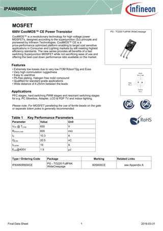
PG-TO220FullPAKWideCreepage
Drain
Pin 2, Tab
Gate
Pin 1
Source
Pin 3
MOSFET
600VCoolMOSªCEPowerTransistor
CoolMOS™isarevolutionarytechnologyforhighvoltagepower
MOSFETs,designedaccordingtothesuperjunction(SJ)principleand
pioneeredbyInfineonTechnologies.CoolMOS™CEisa
price-performanceoptimizedplatformenablingtotargetcostsensitive
applicationsinConsumerandLightingmarketsbystillmeetinghighest
efficiencystandards.Thenewseriesprovidesallbenefitsofafast
switchingSuperjunctionMOSFETwhilenotsacrificingeaseofuseand
offeringthebestcostdownperformanceratioavailableonthemarket.
Features
•ExtremelylowlossesduetoverylowFOMRdson*QgandEoss
•Veryhighcommutationruggedness
•Easytouse/drive
•Pb-freeplating,Halogenfreemoldcompound
•Qualifiedforstandardgradeapplications
•Widedistanceof4.25mmbetweentheleads
Applications
PFCstages,hardswitchingPWMstagesandresonantswitchingstages
fore.g.PCSilverbox,Adapter,LCDPDPTVandindoorlighting.
Pleasenote:ForMOSFETparallelingtheuseofferritebeadsonthegate
orseparatetotempolesisgenerallyrecommended.
Table1KeyPerformanceParameters
Parameter Value Unit
VDS @ Tj,max 650 V
RDS(on),max 600 mΩ
ID. 10.3 A
Qg.typ 20.5 nC
ID,pulse 19 A
Eoss@400V 1.9 µJ
Type/OrderingCode Package Marking RelatedLinks
IPAW60R600CE
PG - TO220 FullPAK
WideCreepage
60S600CE see Appendix A
2. 2
600VCoolMOSªCEPowerTransistor
IPAW60R600CE
2016-03-31Final Data Sheet
TableofContents
Description . . . . . . . . . . . . . . . . . . . . . . . . . . . . . . . . . . . . . . . . . . . . . . . . . . . . . . . . . . . . . . . . . . . . . . . . . . . . . 1
Maximum ratings . . . . . . . . . . . . . . . . . . . . . . . . . . . . . . . . . . . . . . . . . . . . . . . . . . . . . . . . . . . . . . . . . . . . . . . . 3
Thermal characteristics . . . . . . . . . . . . . . . . . . . . . . . . . . . . . . . . . . . . . . . . . . . . . . . . . . . . . . . . . . . . . . . . . . . . 4
Electrical characteristics . . . . . . . . . . . . . . . . . . . . . . . . . . . . . . . . . . . . . . . . . . . . . . . . . . . . . . . . . . . . . . . . . . . 5
Electrical characteristics diagrams . . . . . . . . . . . . . . . . . . . . . . . . . . . . . . . . . . . . . . . . . . . . . . . . . . . . . . . . . . . 7
Test Circuits . . . . . . . . . . . . . . . . . . . . . . . . . . . . . . . . . . . . . . . . . . . . . . . . . . . . . . . . . . . . . . . . . . . . . . . . . . . 11
Package Outlines . . . . . . . . . . . . . . . . . . . . . . . . . . . . . . . . . . . . . . . . . . . . . . . . . . . . . . . . . . . . . . . . . . . . . . . 12
Appendix A . . . . . . . . . . . . . . . . . . . . . . . . . . . . . . . . . . . . . . . . . . . . . . . . . . . . . . . . . . . . . . . . . . . . . . . . . . . . 13
Revision History . . . . . . . . . . . . . . . . . . . . . . . . . . . . . . . . . . . . . . . . . . . . . . . . . . . . . . . . . . . . . . . . . . . . . . . . 14
Trademarks . . . . . . . . . . . . . . . . . . . . . . . . . . . . . . . . . . . . . . . . . . . . . . . . . . . . . . . . . . . . . . . . . . . . . . . . . . . 14
Disclaimer . . . . . . . . . . . . . . . . . . . . . . . . . . . . . . . . . . . . . . . . . . . . . . . . . . . . . . . . . . . . . . . . . . . . . . . . . . . . 14
3. 3
600VCoolMOSªCEPowerTransistor
IPAW60R600CE
2016-03-31Final Data Sheet
1Maximumratings
atTj=25°C,unlessotherwisespecified
Table2Maximumratings
Values
Min. Typ. Max.
Parameter Symbol Unit Note/TestCondition
Continuous drain current1)
ID
-
-
-
-
10.3
6.5
A
TC=25°C
TC=100°C
Pulsed drain current2)
ID,pulse - - 19 A TC=25°C
Avalanche energy, single pulse EAS - - 133 mJ ID=1.3A; VDD=50V; see table 10
Avalanche energy, repetitive EAR - - 0.20 mJ ID=1.3A; VDD=50V; see table 10
Avalanche current, repetitive IAR - - 1.3 A -
MOSFET dv/dt ruggedness dv/dt - - 50 V/ns VDS=0...480V
Gate source voltage (static) VGS -20 - 20 V static;
Gate source voltage (dynamic) VGS -30 - 30 V AC (f1 Hz)
Power dissipation (Full PAK) Ptot - - 28 W TC=25°C
Storage temperature Tstg -40 - 150 °C -
Operating junction temperature Tj -40 - 150 °C -
Mounting torque - - - 50 Ncm M2.5 screws
Continuous diode forward current IS - - 7.3 A TC=25°C
Diode pulse current2)
IS,pulse - - 19 A TC=25°C
Reverse diode dv/dt3)
dv/dt - - 15 V/ns
VDS=0...400V,ISD=IS,Tj=25°C
see table 8
Maximum diode commutation speed dif/dt - - 500 A/µs
VDS=0...400V,ISD=IS,Tj=25°C
see table 8
Power dissipation (Non FullPAK)
TO-220
Ptot - - 82 W -
Insulation withstand voltage for
TO-220FP
VISO - - 2500 V Vrms,TC=25°C,t=1min
1)
Limited by Tj max. Maximum duty cycle D=0.50, TO220 equivalent
2)
Pulse width tp limited by Tj,max
3)
IdenticallowsideandhighsideswitchwithidenticalRG
5. 5
600VCoolMOSªCEPowerTransistor
IPAW60R600CE
2016-03-31Final Data Sheet
3Electricalcharacteristics
atTj=25°C,unlessotherwisespecified
Table4Staticcharacteristics
Values
Min. Typ. Max.
Parameter Symbol Unit Note/TestCondition
Drain-source breakdown voltage V(BR)DSS 600 - - V VGS=0V,ID=0.25mA
Gate threshold voltage V(GS)th 2.5 3.0 3.5 V VDS=VGS,ID=0.2mA
Zero gate voltage drain current IDSS
-
-
-
10
1
-
µA
VDS=600,VGS=0V,Tj=25°C
VDS=600,VGS=0V,Tj=150°C
Gate-source leakage current IGSS - - 100 nA VGS=20V,VDS=0V
Drain-source on-state resistance RDS(on)
-
-
0.54
1.40
0.60
-
Ω
VGS=10V,ID=2.4A,Tj=25°C
VGS=10V,ID=2.4A,Tj=150°C
Gate resistance RG - 10 - Ω f=1MHz,opendrain
Table5Dynamiccharacteristics
Values
Min. Typ. Max.
Parameter Symbol Unit Note/TestCondition
Input capacitance Ciss - 444 - pF VGS=0V,VDS=100V,f=1MHz
Output capacitance Coss - 30 - pF VGS=0V,VDS=100V,f=1MHz
Effective output capacitance,
energy related1) Co(er) - 21 - pF VGS=0V,VDS=0...480V
Effective output capacitance,
time related2) Co(tr) - 88 - pF ID=constant,VGS=0V,VDS=0...480V
Turn-on delay time td(on) - 10 - ns
VDD=400V,VGS=13V,ID=3A,
RG=6.8Ω;seetable9
Rise time tr - 8 - ns
VDD=400V,VGS=13V,ID=3A,
RG=6.8Ω;seetable9
Turn-off delay time td(off) - 58 - ns
VDD=400V,VGS=13V,ID=3A,
RG=6.8Ω;seetable9
Fall time tf - 11 - ns
VDD=400V,VGS=13V,ID=3A,
RG=6.8Ω;seetable9
Table6Gatechargecharacteristics
Values
Min. Typ. Max.
Parameter Symbol Unit Note/TestCondition
Gate to source charge Qgs - 2.5 - nC VDD=480V,ID=3A,VGS=0to10V
Gate to drain charge Qgd - 10.5 - nC VDD=480V,ID=3A,VGS=0to10V
Gate charge total Qg - 20.5 - nC VDD=480V,ID=3A,VGS=0to10V
Gate plateau voltage Vplateau - 5.4 - V VDD=480V,ID=3A,VGS=0to10V
1)
Co(er)isafixedcapacitancethatgivesthesamestoredenergyasCosswhileVDSisrisingfrom0to480V
2)
Co(tr)isafixedcapacitancethatgivesthesamechargingtimeasCosswhileVDSisrisingfrom0to480V
8. 8
600VCoolMOSªCEPowerTransistor
IPAW60R600CE
2016-03-31Final Data Sheet
Diagram5:Typ.outputcharacteristics
VDS[V]
ID[A]
0 5 10 15 20 25
0
5
10
15
20
25
20 V
10 V
8 V
7 V
6 V
5.5 V
5 V
4.5 V
ID=f(VDS);Tj=25°C;parameter:VGS
Diagram6:Typ.outputcharacteristics
VDS[V]
ID[A]
0 5 10 15 20
0
5
10
20 V
10 V
8 V
7 V
6 V
5.5 V
5 V
4.5 V
ID=f(VDS);Tj=125°C;parameter:VGS
Diagram7:Typ.drain-sourceon-stateresistance
ID[A]
RDS(on)[Ω]
0 5 10 15 20
0.80
1.00
1.20
1.40
1.60
1.80
2.00
RDS(on)=f(ID);Tj=125°C;parameter:VGS
Diagram8:Drain-sourceon-stateresistance
Tj[°C]
RDS(on)[Ω]
-40 -15 10 35 60 85 110 135
0.10
0.30
0.50
0.70
0.90
1.10
1.30
1.50
typ
98%
RDS(on)=f(Tj);ID=2.4A;VGS=10V
12. 12
600VCoolMOSªCEPowerTransistor
IPAW60R600CE
2016-03-31Final Data Sheet
6PackageOutlines
MILLIMETERS
4.25 (BSC)
c
D
E
D1
L1
e
L
N
b2
A
A1
b
A2
DIM
0.40
1.70
15.47
9.17
10.70
12.58
3
MIN
4.50
2.34
0.75
2.65
0.609
0.361
0.421
0.016
0.177
0.092
0.030
0.104
0.495
0.60
16.27
11.30
13.38
2.30
4.90
2.74
0.90
2.95
MAX
0.024
3
0.641
0.445
0.527
0.091
INCHES
MIN MAX
0.193
0.108
0.035
0.116
EUROPEAN PROJECTION
ISSUE DATE
0
SCALE
4 mm
REVISION
28-04-2015
01
DOCUMENT NO.
0.167 (BSC)
0.067
0.98 0.0391.26 0.050
3.00 0.1183.30 0.130
b3
b5 3.00 0.118- -
1.00 0.0391.40 0.055
DIMENSIONS DO NOT INCLUDE MOLD FLASH, PROTRUSIONS OR GATE BURRS
E
D
D1
L1
H
b2
b
b5
b3
P
c
A
A1
Q
A2
0
2
2
L0.381 B A
e
Q 3.10 3.50 0.1380.122
H 28.25 1.11229.45 1.159
Z8B00176938
Figure1OutlinePG-TO220FullPAKWideCreepage,dimensionsinmm/inches
14. 14
600VCoolMOSªCEPowerTransistor
IPAW60R600CE
2016-03-31Final Data Sheet
RevisionHistory
IPAW60R600CE
Revision:2016-03-31
Previous Revision
Date Subjects (major changes since last revision)
2015-10-07 Release of final version
2015-10-28 Revised electrical characteristics
2016-03-31 Modified Id ratings
TrademarksofInfineonTechnologiesAG
AURIX™,C166™,CanPAK™,CIPOS™,CoolGaN™,CoolMOS™,CoolSET™,CoolSiC™,CORECONTROL™,CROSSAVE™,DAVE™,DI-POL™,DrBlade™,
EasyPIM™,EconoBRIDGE™,EconoDUAL™,EconoPACK™,EconoPIM™,EiceDRIVER™,eupec™,FCOS™,HITFET™,HybridPACK™,Infineon™,
ISOFACE™,IsoPACK™,i-Wafer™,MIPAQ™,ModSTACK™,my-d™,NovalithIC™,OmniTune™,OPTIGA™,OptiMOS™,ORIGA™,POWERCODE™,
PRIMARION™,PrimePACK™,PrimeSTACK™,PROFET™,PRO-SIL™,RASIC™,REAL3™,ReverSave™,SatRIC™,SIEGET™,SIPMOS™,SmartLEWIS™,
SOLIDFLASH™,SPOC™,TEMPFET™,thinQ™,TRENCHSTOP™,TriCore™.
TrademarksupdatedAugust2015
OtherTrademarks
Allreferencedproductorservicenamesandtrademarksarethepropertyoftheirrespectiveowners.
WeListentoYourComments
Anyinformationwithinthisdocumentthatyoufeeliswrong,unclearormissingatall?Yourfeedbackwillhelpustocontinuously
improvethequalityofthisdocument.Pleasesendyourproposal(includingareferencetothisdocument)to:
erratum@infineon.com
Publishedby
InfineonTechnologiesAG
81726München,Germany
©2016InfineonTechnologiesAG
AllRightsReserved.
LegalDisclaimer
Theinformationgiveninthisdocumentshallinnoeventberegardedasaguaranteeofconditionsorcharacteristics.With
respecttoanyexamplesorhintsgivenherein,anytypicalvaluesstatedhereinand/oranyinformationregardingtheapplication
ofthedevice,InfineonTechnologiesherebydisclaimsanyandallwarrantiesandliabilitiesofanykind,includingwithout
limitation,warrantiesofnon-infringementofintellectualpropertyrightsofanythirdparty.
Information
Forfurtherinformationontechnology,deliverytermsandconditionsandpricespleasecontactyournearestInfineon
TechnologiesOffice(www.infineon.com).
Warnings
Duetotechnicalrequirements,componentsmaycontaindangeroussubstances.Forinformationonthetypesinquestion,
pleasecontactthenearestInfineonTechnologiesOffice.
TheInfineonTechnologiescomponentdescribedinthisDataSheetmaybeusedinlife-supportdevicesorsystemsand/or
automotive,aviationandaerospaceapplicationsorsystemsonlywiththeexpresswrittenapprovalofInfineonTechnologies,ifa
failureofsuchcomponentscanreasonablybeexpectedtocausethefailureofthatlife-support,automotive,aviationand
aerospacedeviceorsystemortoaffectthesafetyoreffectivenessofthatdeviceorsystem.Lifesupportdevicesorsystemsare
intendedtobeimplantedinthehumanbodyortosupportand/ormaintainandsustainand/orprotecthumanlife.Iftheyfail,itis
reasonabletoassumethatthehealthoftheuserorotherpersonsmaybeendangered.