Downloaded 107 times
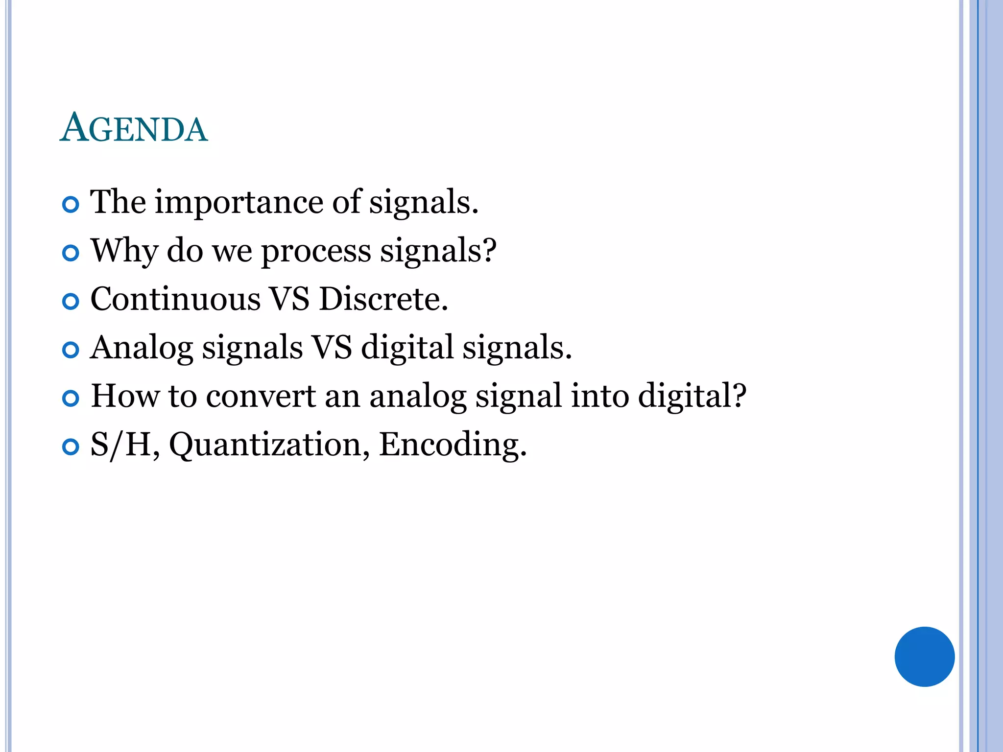
![WHAT ARE SIGNALS?
Signals are mathematical functions that represents an
electrical quantity (voltage, current ..etc).
These quantity carries information in one of its
parameters [amplitude, frequency ..etc].](https://image.slidesharecdn.com/interfacingtotheanalogworld-131206175956-phpapp01/75/Interfacing-to-the-analog-world-3-2048.jpg)
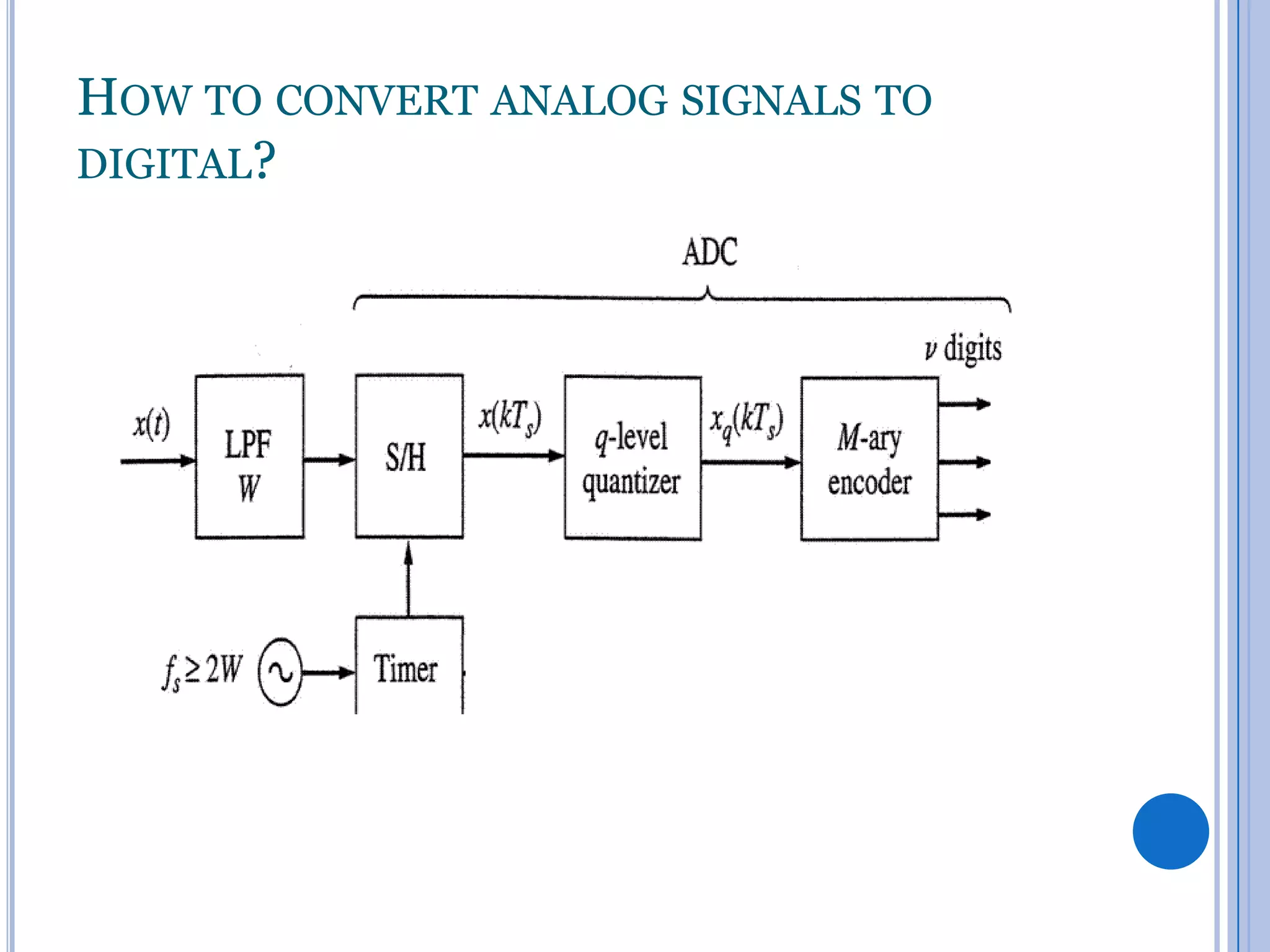
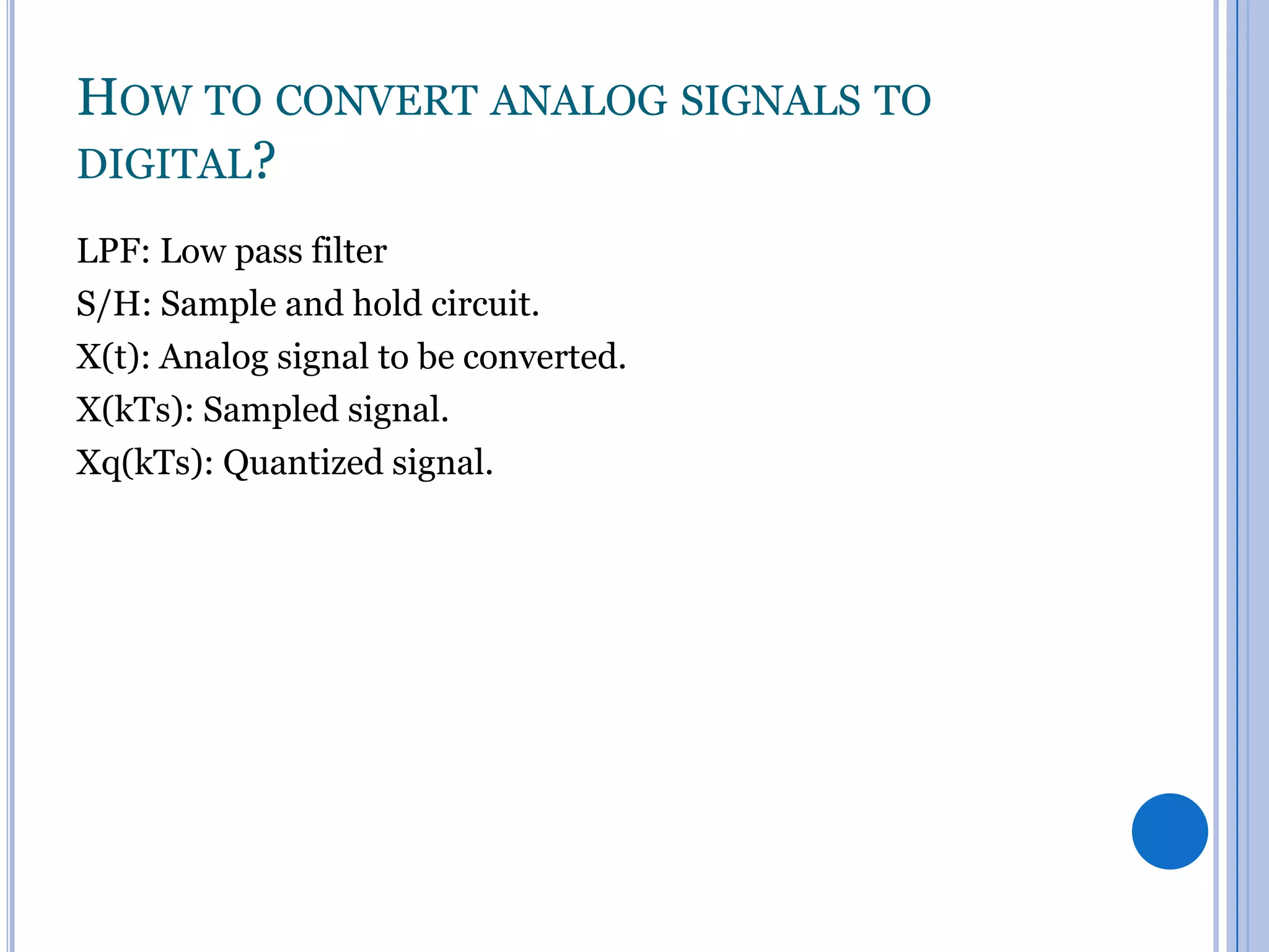
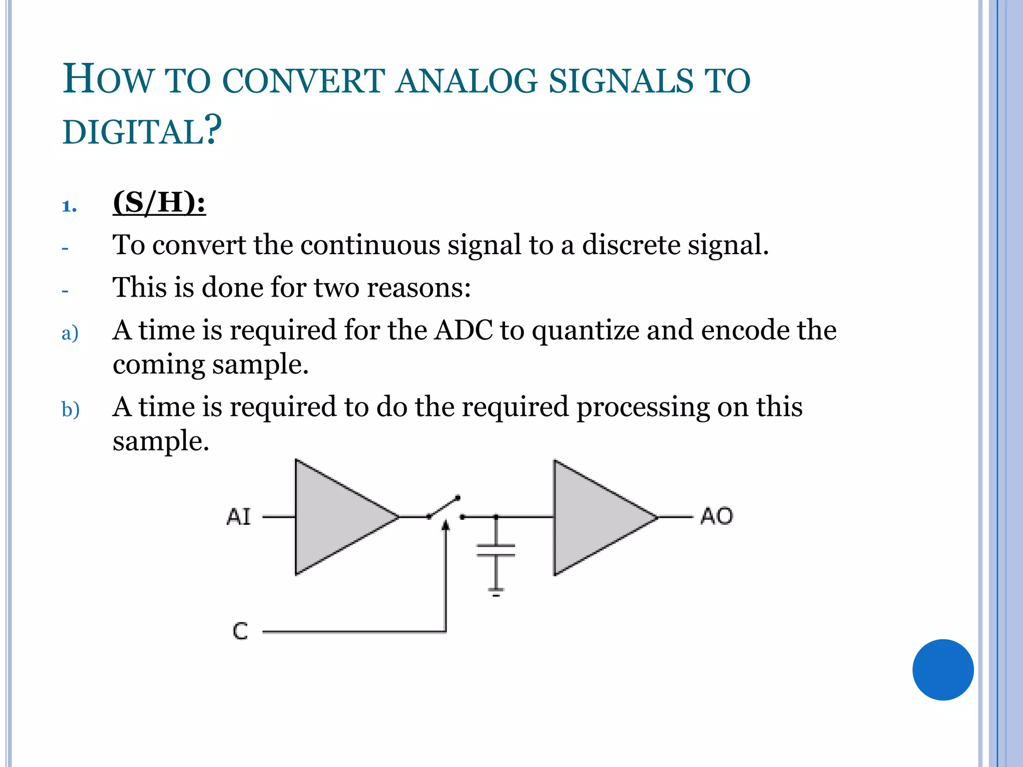
![HOW TO CONVERT ANALOG SIGNALS TO
DIGITAL?
1.
LPF: The signal is filtered and band limited to 0.5 Fs, in
order to avoid aliasing. (Review sampling theorem)
Fs≥2Fm
[Nyquist rate]
Fm: the max. signal frequency.
-
1.
2.
If the sampled signal is not band limited, aliasing will occur.
This will result:
The digital signal produced is not representing the original
analog signal.
If we tried to reproduce the analog signal it’ll be distorted.](https://image.slidesharecdn.com/interfacingtotheanalogworld-131206175956-phpapp01/75/Interfacing-to-the-analog-world-15-2048.jpg)
![SIGNAL CONDITIONING
Typical sensors yield low-amplitude analog signals that need to be
amplified and then digitized by means of an (A/D) converter.
To adapt the analog signal to the range of expected amplitude at the
input of the A/D converter, a signal conditioner is used.
Ex. If the analog signal in the range: [-20mv 20mv]
and the ADC is [0v 5v]
-
The number of values that represent this analog range is small, so
that the quantization noise will be large.
-
If we amplified the signal by (*100) , it’ll be in the range: [-2v 2v]
and the quantization noise is reduced.](https://image.slidesharecdn.com/interfacingtotheanalogworld-131206175956-phpapp01/75/Interfacing-to-the-analog-world-26-2048.jpg)
![SIGNAL CONDITIONING
-
If the analog signal can be +ve or –ve, use a shift up circuit (adder) to
make it in the range [0v Vref v].](https://image.slidesharecdn.com/interfacingtotheanalogworld-131206175956-phpapp01/75/Interfacing-to-the-analog-world-27-2048.jpg)

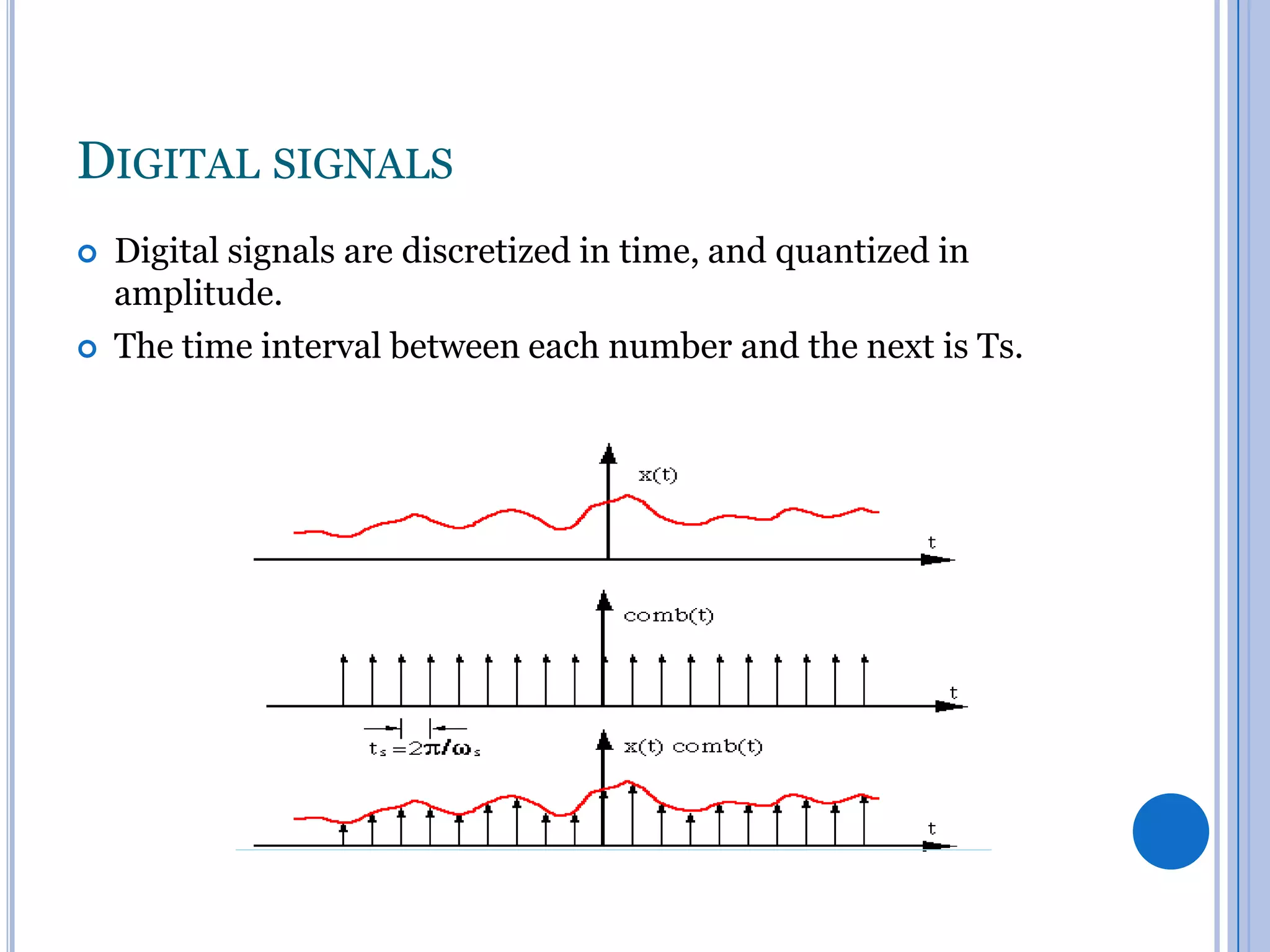
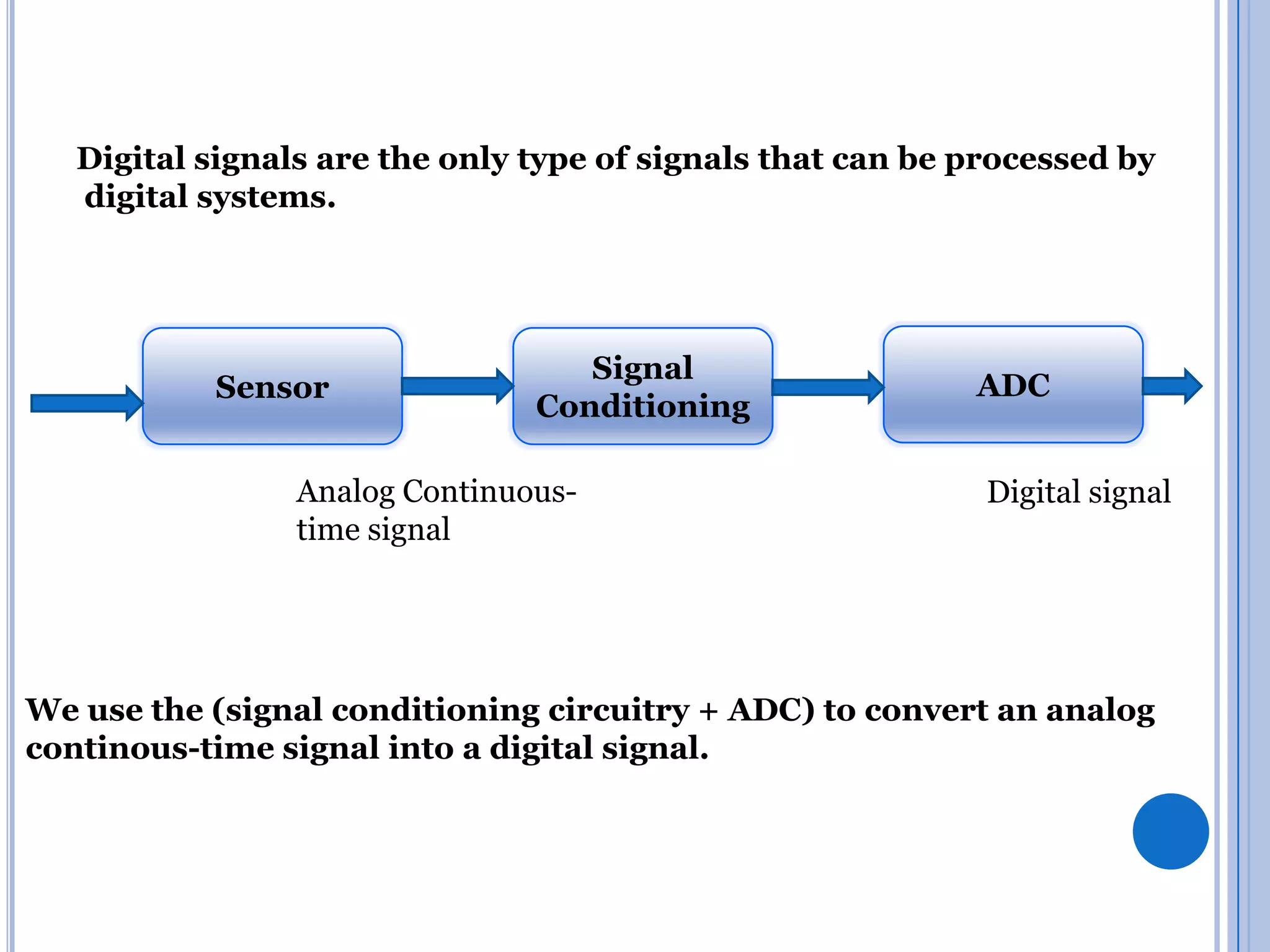
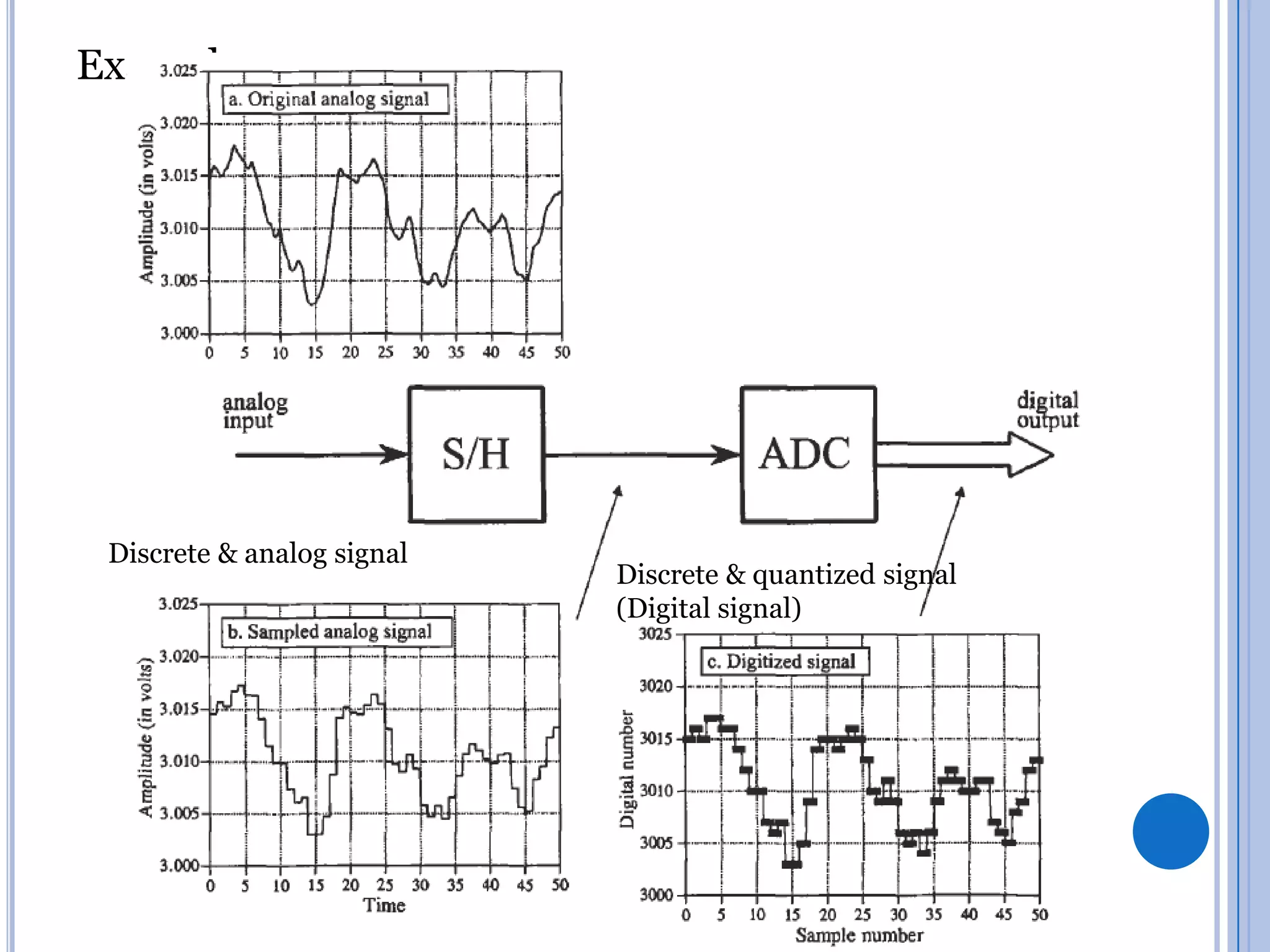
The document discusses analog to digital conversion. It explains that analog signals are continuous while digital signals are discrete in both time and amplitude. It describes how analog signals are converted to digital using sample and hold circuits, quantization, and encoding. The conversion process filters the analog signal, takes samples at regular time intervals, rounds samples to the nearest digital value, and encodes samples into binary format. The document also provides examples of analog to digital converters and discusses considerations like resolution, dynamic range, and signal conditioning.