SlideShare a Scribd company logo
1 of 3
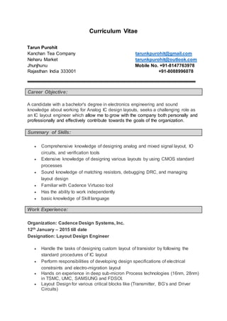
Curriculum Vitae
Tarun Purohit
Kanchan Tea Company tarunkpurohit@gmail.com
Neharu Market tarunkpurohit@outlook.com
Jhunjhunu Mobile No. +91-8147763978
Rajasthan India 333001 +91-8088996078
Career Objective:
A candidate with a bachelor's degree in electronics engineering and sound
knowledge about working for Analog IC design layouts, seeks a challenging role as
an IC layout engineer which allow me to grow with the company both personally and
professionally and effectively contribute towards the goals of the organization.
Summary of Skills:
 Comprehensive knowledge of designing analog and mixed signal layout, IO
circuits, and verification tools
 Extensive knowledge of designing various layouts by using CMOS standard
processes
 Sound knowledge of matching resistors, debugging DRC, and managing
layout design
 Familiar with Cadence Virtuoso tool
 Has the ability to work independently
 basic knowledge of Skill language
Work Experience:
Organization: Cadence Design Systems, Inc.
12th January – 2015 till date
Designation: Layout Design Engineer
 Handle the tasks of designing custom layout of transistor by following the
standard procedures of IC layout
 Perform responsibilities of developing design specifications of electrical
constraints and electro-migration layout
 Hands on experience in deep sub-micron Process technologies (16nm, 28nm)
in TSMC, UMC, SAMSUNG and FDSOI.
 Layout Design for various critical blocks like (Transmitter, BG’s and Driver
Circuits)
 Responsible for coordinating with design engineers to ensure that the
designed layout of electrical chips meets the standard guidelines
 Handle responsibilities of updating IC design to the senior engineer for
verification
 Responsible for developing custom IC layout by utilizing Cadence layout tools
Organization: Cadence Design Systems, Inc.
30 April 2014 – 11 Jan 2015
Designation: Analog layout Consultant
 Hands on experience in deep sub-micron Process technologies (16nm, 28nm)
in TSMC, UMC, SAMSUNG and FDSOI.
 Layout Design for various critical blocks like (LDO and Sampler Circuits)
 Assigned the tasks of assisting senior IC layout engineer in generating quality
layouts following by following the standard methods
 Performed the tasks of developing IC layout from scratch as well as verified
IC by using CAD tools
 Performed the task of developing custom layouts under the guidelines of
senior IC layout engineer
Organization: Cadence Design Systems, Inc.
30 Sept 2013 – 29 April 2014
Designation: Analog Layout Design Trainee
 Undergone Seven months of Analog and Mixed signal Layout Design training.
 Learned about Physical verification flow (DRC, LVS and QRC) in PVS.
 Worked on Simulations for small circuits and verified the results.
Educational Qualifications:
 Bachelor of Technology in Electronics and Communication Engineering
Rajasthan Technical University in the year 2013
Declaration:
I hereby certify that all the information provided above is true to the best of my
knowledge.
Date:
Place: Bangalore Tarun Purohit

More Related Content

What's hot (20)

Venkat
VenkatVenkat
Venkat
 
Ghanshyam_CV latest
Ghanshyam_CV latestGhanshyam_CV latest
Ghanshyam_CV latest
 
resume document_updated
resume document_updatedresume document_updated
resume document_updated
 
NISHANT COVER LETTER
NISHANT COVER LETTERNISHANT COVER LETTER
NISHANT COVER LETTER
 
Abd Al Monam 2016 photo
Abd Al Monam 2016 photoAbd Al Monam 2016 photo
Abd Al Monam 2016 photo
 
Abd Al Monam 2016
Abd Al Monam 2016Abd Al Monam 2016
Abd Al Monam 2016
 
Neeraj Srivastava
Neeraj SrivastavaNeeraj Srivastava
Neeraj Srivastava
 
Resume (1)
Resume (1)Resume (1)
Resume (1)
 
Sunil (Instrumentation)-1
Sunil (Instrumentation)-1Sunil (Instrumentation)-1
Sunil (Instrumentation)-1
 
Updated resume
Updated resumeUpdated resume
Updated resume
 
Resume_Venkatesh
Resume_VenkateshResume_Venkatesh
Resume_Venkatesh
 
RESUME SCHNEIDER
RESUME SCHNEIDERRESUME SCHNEIDER
RESUME SCHNEIDER
 
Jody resume EET
Jody resume EETJody resume EET
Jody resume EET
 
vivek_Resume
vivek_Resumevivek_Resume
vivek_Resume
 
Resume
ResumeResume
Resume
 
Photo resume 131115
Photo resume 131115Photo resume 131115
Photo resume 131115
 
Mohammed Irfan cv (1)
Mohammed Irfan cv (1)Mohammed Irfan cv (1)
Mohammed Irfan cv (1)
 
Resume 2016 Dec
Resume 2016 DecResume 2016 Dec
Resume 2016 Dec
 
ABDUL NATHIQ RESUME updated
ABDUL NATHIQ RESUME updatedABDUL NATHIQ RESUME updated
ABDUL NATHIQ RESUME updated
 
Omar_Afia_Resume2015ae_NETWORK (English)
Omar_Afia_Resume2015ae_NETWORK (English)Omar_Afia_Resume2015ae_NETWORK (English)
Omar_Afia_Resume2015ae_NETWORK (English)
 

Viewers also liked

Flash
FlashFlash
Flashhccit
 
Photoshop
PhotoshopPhotoshop
Photoshophccit
 
Ask manual rev5
Ask manual rev5Ask manual rev5
Ask manual rev5hccit
 
La millor consola
La millor consolaLa millor consola
La millor consolaJowel35
 
Hukum di Indonesia Saat Ini
Hukum di Indonesia Saat IniHukum di Indonesia Saat Ini
Hukum di Indonesia Saat IniFatchul Amin
 
Jg all
Jg allJg all
Jg allhccit
 
Creating l ainmypls
Creating l ainmyplsCreating l ainmypls
Creating l ainmyplshccit
 
Final documentation major proj_js
Final documentation major proj_jsFinal documentation major proj_js
Final documentation major proj_jshccit
 
콜링 벤쳐경연 소개2014 slideshow
콜링 벤쳐경연 소개2014 slideshow콜링 벤쳐경연 소개2014 slideshow
콜링 벤쳐경연 소개2014 slideshowPatrick Cha
 

Viewers also liked (13)

Flash
FlashFlash
Flash
 
Photoshop
PhotoshopPhotoshop
Photoshop
 
Ask manual rev5
Ask manual rev5Ask manual rev5
Ask manual rev5
 
La millor consola
La millor consolaLa millor consola
La millor consola
 
Hukum di Indonesia Saat Ini
Hukum di Indonesia Saat IniHukum di Indonesia Saat Ini
Hukum di Indonesia Saat Ini
 
Jg all
Jg allJg all
Jg all
 
09 chapter 4
09 chapter 409 chapter 4
09 chapter 4
 
Actividades letra z 1
Actividades letra z 1Actividades letra z 1
Actividades letra z 1
 
Creating l ainmypls
Creating l ainmyplsCreating l ainmypls
Creating l ainmypls
 
Final documentation major proj_js
Final documentation major proj_jsFinal documentation major proj_js
Final documentation major proj_js
 
Actividades letra c 1
Actividades letra c 1Actividades letra c 1
Actividades letra c 1
 
콜링 벤쳐경연 소개2014 slideshow
콜링 벤쳐경연 소개2014 slideshow콜링 벤쳐경연 소개2014 slideshow
콜링 벤쳐경연 소개2014 slideshow
 
Actividades letra b
Actividades letra b Actividades letra b
Actividades letra b
 

Similar to CV Tarun Purohit Electronics Engineer IC Layout

AnilSubhas_11.7 Yrs_Electrical-systems-Engineer.pdf
AnilSubhas_11.7 Yrs_Electrical-systems-Engineer.pdfAnilSubhas_11.7 Yrs_Electrical-systems-Engineer.pdf
AnilSubhas_11.7 Yrs_Electrical-systems-Engineer.pdfANIL SUBHAS
 
jawed_CV_instrument 3.7 yr exp
jawed_CV_instrument 3.7 yr expjawed_CV_instrument 3.7 yr exp
jawed_CV_instrument 3.7 yr expjawed ali
 
Rajesh K G CV-ECE
Rajesh K G CV-ECERajesh K G CV-ECE
Rajesh K G CV-ECERajesh K G
 
Rajesh K G CV-ECE
Rajesh K G CV-ECERajesh K G CV-ECE
Rajesh K G CV-ECERajesh K G
 
Rajesh K G CV-ECE
Rajesh K G CV-ECERajesh K G CV-ECE
Rajesh K G CV-ECERajesh K G
 
Different Job Roles after Electronics and Communication Engineering
Different Job Roles after Electronics and Communication EngineeringDifferent Job Roles after Electronics and Communication Engineering
Different Job Roles after Electronics and Communication EngineeringDIT University
 
CV-Krushna Ch. Parida_Design engineer (Electrical)
CV-Krushna Ch. Parida_Design engineer (Electrical)CV-Krushna Ch. Parida_Design engineer (Electrical)
CV-Krushna Ch. Parida_Design engineer (Electrical)Krushna Parida
 
Krishnakumar signalling
Krishnakumar signallingKrishnakumar signalling
Krishnakumar signallingKrishna Kumar
 
Jibin manual resume
Jibin manual resumeJibin manual resume
Jibin manual resumeJibin Manual
 
Amal U S(Asp.Net Web Developer)
Amal U S(Asp.Net Web Developer)Amal U S(Asp.Net Web Developer)
Amal U S(Asp.Net Web Developer)Amal U S
 
CV (M Tech)
CV (M Tech) CV (M Tech)
CV (M Tech) Arquam Md
 

Similar to CV Tarun Purohit Electronics Engineer IC Layout (20)

AnilSubhas_11.7 Yrs_Electrical-systems-Engineer.pdf
AnilSubhas_11.7 Yrs_Electrical-systems-Engineer.pdfAnilSubhas_11.7 Yrs_Electrical-systems-Engineer.pdf
AnilSubhas_11.7 Yrs_Electrical-systems-Engineer.pdf
 
jawed_CV_instrument 3.7 yr exp
jawed_CV_instrument 3.7 yr expjawed_CV_instrument 3.7 yr exp
jawed_CV_instrument 3.7 yr exp
 
Mani Final Resume
Mani Final ResumeMani Final Resume
Mani Final Resume
 
Resume
ResumeResume
Resume
 
Resume
ResumeResume
Resume
 
Rajesh K G CV-ECE
Rajesh K G CV-ECERajesh K G CV-ECE
Rajesh K G CV-ECE
 
Rajesh K G CV-ECE
Rajesh K G CV-ECERajesh K G CV-ECE
Rajesh K G CV-ECE
 
Rajesh K G CV-ECE
Rajesh K G CV-ECERajesh K G CV-ECE
Rajesh K G CV-ECE
 
Different Job Roles after Electronics and Communication Engineering
Different Job Roles after Electronics and Communication EngineeringDifferent Job Roles after Electronics and Communication Engineering
Different Job Roles after Electronics and Communication Engineering
 
CV-Krushna Ch. Parida_Design engineer (Electrical)
CV-Krushna Ch. Parida_Design engineer (Electrical)CV-Krushna Ch. Parida_Design engineer (Electrical)
CV-Krushna Ch. Parida_Design engineer (Electrical)
 
Resume1
Resume1Resume1
Resume1
 
Jagadeesh vlsi cv
Jagadeesh vlsi cvJagadeesh vlsi cv
Jagadeesh vlsi cv
 
Vignesh Resume
Vignesh ResumeVignesh Resume
Vignesh Resume
 
Krishnakumar signalling
Krishnakumar signallingKrishnakumar signalling
Krishnakumar signalling
 
Karthic 2015
Karthic 2015Karthic 2015
Karthic 2015
 
Jibin manual resume
Jibin manual resumeJibin manual resume
Jibin manual resume
 
resume
resumeresume
resume
 
Amal U S(Asp.Net Web Developer)
Amal U S(Asp.Net Web Developer)Amal U S(Asp.Net Web Developer)
Amal U S(Asp.Net Web Developer)
 
CV (M Tech)
CV (M Tech) CV (M Tech)
CV (M Tech)
 
RESUME REV.05
RESUME REV.05RESUME REV.05
RESUME REV.05
 

CV Tarun Purohit Electronics Engineer IC Layout

  • 1. Curriculum Vitae Tarun Purohit Kanchan Tea Company tarunkpurohit@gmail.com Neharu Market tarunkpurohit@outlook.com Jhunjhunu Mobile No. +91-8147763978 Rajasthan India 333001 +91-8088996078 Career Objective: A candidate with a bachelor's degree in electronics engineering and sound knowledge about working for Analog IC design layouts, seeks a challenging role as an IC layout engineer which allow me to grow with the company both personally and professionally and effectively contribute towards the goals of the organization. Summary of Skills:  Comprehensive knowledge of designing analog and mixed signal layout, IO circuits, and verification tools  Extensive knowledge of designing various layouts by using CMOS standard processes  Sound knowledge of matching resistors, debugging DRC, and managing layout design  Familiar with Cadence Virtuoso tool  Has the ability to work independently  basic knowledge of Skill language Work Experience: Organization: Cadence Design Systems, Inc. 12th January – 2015 till date Designation: Layout Design Engineer  Handle the tasks of designing custom layout of transistor by following the standard procedures of IC layout  Perform responsibilities of developing design specifications of electrical constraints and electro-migration layout  Hands on experience in deep sub-micron Process technologies (16nm, 28nm) in TSMC, UMC, SAMSUNG and FDSOI.  Layout Design for various critical blocks like (Transmitter, BG’s and Driver Circuits)
  • 2.  Responsible for coordinating with design engineers to ensure that the designed layout of electrical chips meets the standard guidelines  Handle responsibilities of updating IC design to the senior engineer for verification  Responsible for developing custom IC layout by utilizing Cadence layout tools Organization: Cadence Design Systems, Inc. 30 April 2014 – 11 Jan 2015 Designation: Analog layout Consultant  Hands on experience in deep sub-micron Process technologies (16nm, 28nm) in TSMC, UMC, SAMSUNG and FDSOI.  Layout Design for various critical blocks like (LDO and Sampler Circuits)  Assigned the tasks of assisting senior IC layout engineer in generating quality layouts following by following the standard methods  Performed the tasks of developing IC layout from scratch as well as verified IC by using CAD tools  Performed the task of developing custom layouts under the guidelines of senior IC layout engineer Organization: Cadence Design Systems, Inc. 30 Sept 2013 – 29 April 2014 Designation: Analog Layout Design Trainee  Undergone Seven months of Analog and Mixed signal Layout Design training.  Learned about Physical verification flow (DRC, LVS and QRC) in PVS.  Worked on Simulations for small circuits and verified the results. Educational Qualifications:  Bachelor of Technology in Electronics and Communication Engineering Rajasthan Technical University in the year 2013 Declaration: I hereby certify that all the information provided above is true to the best of my knowledge. Date: