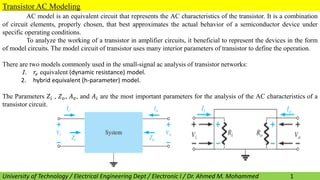
1. AC model is an equivalent circuit that represents the AC characteristics of the transistor. It is a combination
of circuit elements, properly chosen, that best approximates the actual behavior of a semiconductor device under
specific operating conditions.
To analyze the working of a transistor in amplifier circuits, it beneficial to represent the devices in the form
of model circuits. The model circuit of transistor uses many interior parameters of transistor to define the operation.
There are two models commonly used in the small-signal ac analysis of transistor networks:
1. 𝑟𝑒 equivalent (dynamic resistance) model.
2. hybrid equivalent (h-parameter) model.
The Parameters 𝑍𝑖 , 𝑍𝑜, 𝐴𝑣, and 𝐴𝑖 are the most important parameters for the analysis of the AC characteristics of a
transistor circuit.
University of Technology / Electrical Engineering Dept / Electronic I / Dr. Ahmed M. Mohammed
Transistor AC Modeling
1
2. Important procedures for ac analysis (small signal analysis)
1. Setting all dc sources to zero and replacing them by a short-circuit equivalent
2. Replacing all capacitors by a short-circuit equivalent
3. Removing all elements bypassed by the short-circuit equivalents introduced by steps 1 and 2
4. Redrawing the network in a more convenient and logical form.
5. Defining the important parameters of the transistor model.
University of Technology / Electrical Engineering Dept / Electronic I / Dr. Ahmed M. Mohammed
Transistor AC Modeling
2
4. Common-Emitter Configuration
The equivalent circuit for the common-emitter configuration will be constructed using the device characteristics and a
number of approximations. Starting with the input side, we find the applied voltage 𝑽𝒊 is equal to the voltage 𝑽𝒃𝒆
(0.7) with the input current being the base current 𝑰𝒃.
If we redraw the collector characteristics to have a constant 𝜷 (another approximation), the entire characteristics at the
output section can be replaced by a current controlled source whose magnitude is beta times the base current.
Because all the input and output parameters of the original configuration are now present, the equivalent network for
the common-emitter configuration has been established.
The equivalent model can be improved by first replacing the diode by its equivalent resistance 𝒓𝒅 =
𝟐𝟔𝒎𝑽
𝑰𝑫
.
Using the subscript e because the determining current is the emitter current will result in 𝒓𝒆 =
𝟐𝟔𝒎𝑽
𝑰𝑬
𝑍𝑖 =
𝑉𝑖
𝐼𝑏
=
𝑉𝑏𝑒
𝐼𝑏
𝑉𝑏𝑒 = 𝐼𝑒𝑟𝑒 = 𝐼𝑐 + 𝐼𝑏 𝑟𝑒
𝑉𝑏𝑒 = 𝛽𝐼𝑏 + 𝐼𝑏 𝑟𝑒 = 𝛽 + 1 𝐼𝑏𝑟𝑒
𝑍𝑖 =
𝑉𝑏𝑒
𝐼𝑏
=
𝛽+1 𝐼𝑏𝑟𝑒
𝐼𝑏
University of Technology / Electrical Engineering Dept / Electronic I / Dr. Ahmed M. Mohammed
The 𝒓𝒆Transistor Model
4
5. The result is that the impedance seen “looking into” the base of the network is a resistor equal to
beta times the value of 𝒓𝒆. The collector output current is still linked to the input current by beta
as shown in the same figure.
The output impedance 𝒓𝒐 can be calculated and it is appear as a resistor in parallel with the output
as shown in the equivalent circuit.
For the common-emitter configuration there is a 180 ° phase shift.
University of Technology / Electrical Engineering Dept / Electronic I / Dr. Ahmed M. Mohammed 5
6. Common-Base Configuration
The common-base equivalent circuit will be developed in much the same manner as applied to the
common-emitter configuration.
For the ac response, the diode can be replaced by its equivalent ac resistance determined by
The network of is an excellent equivalent circuit for the analysis of most common-base configurations. It is
similar in many ways to that of the common-emitter configuration.
In general, common-base configurations have very low input impedance because it is essentially simply
𝒓𝒆. Typical values extend from a few ohms to perhaps 50Ω. The output impedance 𝑟𝑜 will typically extend
into the mega ohm range.
Because the output current is opposite to the defined 𝐼𝑜 direction, you will find in the analysis to follow
that there is no phase shift between the input and output voltages.
University of Technology / Electrical Engineering Dept / Electronic I / Dr. Ahmed M. Mohammed 6
7. Common Emitter, Fixed Bias Configuration
Circuit analysis
Input impedance (𝒁𝒊)
𝒁𝒊 = 𝑹𝑩 ∖∖ 𝛃𝒓𝒆
(For 𝑹𝑩 larger than 10 𝜷𝒓𝒆)
𝑍𝑖 ≅ 𝛽𝑟𝑒
Output impedance (𝒁𝒐)
𝒁𝒐 = 𝑹𝑪 ∖∖ 𝒓𝒐
(For 𝒓𝒐 larger than 10𝑹𝑪)
𝑍o ≅ 𝑅C
Voltage gain (𝑨𝑽)
𝐴𝑣 =
𝑉𝑜
𝑉𝑖
𝑉
𝑜 = −𝛽𝐼𝑏 𝑅𝐶 ∖∖ 𝑟𝑜
𝑉𝑖 = 𝐼𝑏𝛽𝑟𝑒
𝐴𝑣 =
𝑉𝑜
𝑉𝑖
=
−𝛽𝐼𝑏 𝑅𝐶∖∖𝑟𝑜
𝛽𝐼𝑏𝑟𝑒
If 𝒓𝒐 ≫ 𝟏𝟎𝑹𝑪, so that the effect of 𝑟𝑜 can be ignored,
University of Technology / Electrical Engineering Dept / Electronic I / Dr. Ahmed M. Mohammed 7
8. EXAMPLE 1
For the network shown in the Figure determine:
a) Determine 𝑟𝑒.
b) Determine 𝑍𝑖, 𝑍𝑜 and 𝐴𝑣 (with 𝑟𝑜 = ∞).
c) Repeat parts (b) including (𝑟𝑜 = 50 𝑘Ω).
Solution:
a) 𝐼𝐵 =
𝑉𝐶𝐶−𝑉𝐵𝐸
𝑅𝐵
=
12 𝑉−0.7 𝑉
470 𝑘Ω
= 24.04 𝜇𝐴
𝐼𝐸 = 𝛽 + 1 𝐼𝐵 = 100 + 1 24.04𝑚𝐴 = 2.428𝑚𝐴
𝑟𝑒 =
26 𝑚𝑉
𝐼𝑒
=
26𝑚𝑉
2.428 𝑚𝐴
= 10.71 Ω
b) 𝑍𝑖 = 𝑅𝐵 ∖∖ 𝛽𝑟𝑒 = 1.07 𝑘Ω
𝑍o = 𝑅C ∖∖ 𝑟o = 3𝑘Ω ∖∖ ∞ = 𝑅C = 3 𝑘Ω
𝐴𝑣 =
− 𝑅𝐶∖∖𝑟𝑜
𝑟𝑒
=
−𝑅𝐶
𝑟𝑒
=
−3 𝑘Ω
10.7 Ω
= −280.1
c) 𝑍o = 𝑅C ∖∖ 𝑟o = 3𝑘Ω ∖∖ 50𝑘Ω = 2.83 𝑘Ω
𝐴𝑣 =
− 𝑅𝐶∖∖𝑟𝑜
𝑟𝑒
=
−3 𝑘Ω∖∖50 𝑘Ω
10.7 Ω
= −264.24
University of Technology / Electrical Engineering Dept / Electronic I / Dr. Ahmed M. Mohammed 8
9. Common Emitter, Voltage Divider Bias Configuration
𝑹𝟏 and 𝑹𝟐 remain part of the input circuit, whereas 𝑅𝐶 is part of the output circuit. The parallel
combination of 𝑅1 and 𝑅2 is defined by 𝑹′ = 𝑹𝟏 ∥ 𝑹𝟐.
Input impedance (𝒁𝒊)
For large 𝑅𝐵 (larger than 10 𝛽𝑟𝑒) 𝑍𝑖 ≅ 𝛽𝑟𝑒
Output impedance (𝒁𝒐)
For 𝑟o larger than 10RC) 𝑍o ≅ 𝑅C
Voltage gain (𝑨𝑽)
Electrical Engineering Dept / Year Two / Semester I / Electronic I / Dr. Ahmed M. Mohammed 9
10. EXAMPLE 2
For the network shown in the Figure determine:
a) Determine 𝑟𝑒.
b) Determine 𝑍𝑖, 𝑍𝑜 and 𝐴𝑣 (with 𝑟𝑜 = ∞).
c) Repeat parts (b) including (𝑟𝑜 = 50 𝑘Ω).
Solution
a) 𝑉𝐵 = 𝑉𝐶𝐶 .
𝑅2
𝑅1+𝑅2
= 22
8.2𝑘Ω
56+8.2 𝑘Ω
= 2.81 𝑉
𝑉𝐸 = 𝑉𝐵 − 𝑉𝐵𝐸 = 2.81 − 0.7 = 2.11 𝑉
𝐼𝐸 =
𝑉𝐸
𝑅𝐸
=
2.11 𝑉
1.5 𝑘Ω
= 1.41 𝑚𝐴
𝑟𝑒 =
26𝑚𝑉
1.41 𝑚𝐴
= 18.44 Ω
b) 𝑅′ = 𝑅1 ∥ 𝑅2 = 7.15 𝑘Ω
𝑍𝑖 = 𝑅′ ∖∖ 𝛽𝑟𝑒 = 1.35 𝑘Ω
𝑍o = 𝑅C ∖∖ 𝑟o = 𝑅C = 6.8 𝑘Ω
𝐴𝑣 =
− 𝑅𝐶∖∖𝑟𝑜
𝑟𝑒
=
−𝑅𝐶
𝑟𝑒
=
−6.8 𝑘Ω
18.44 Ω
= −368.76
c) ???
University of Technology / Electrical Engineering Dept / Electronic I / Dr. Ahmed M. Mohammed 10
11. CE Emitter-Base Configuration with 𝑅𝐸 (Unbypassed circuit analysis)
Applying Kirchhoff’s voltage law to the input side
𝑉𝑖 = 𝐼𝑏𝛽𝑟𝑒 + 𝐼𝑒𝑅𝐸
𝑉𝑖 = 𝐼𝑏𝛽𝑟𝑒 + (𝛽 + 1)𝐼𝑏𝑅𝐸
the input impedance looking into the network to the right of 𝑅𝐵is:-
𝑍𝑏 =
𝑉𝑖
𝐼𝑖
=
𝐼𝑏[𝛽𝑟𝑒+ 𝛽+1 𝑅𝐸]
𝐼𝑏
= 𝛽𝑟𝑒 + 𝛽 + 1 𝑅𝐸
for
for
University of Technology / Electrical Engineering Dept / Electronic I / Dr. Ahmed M. Mohammed 11
12. Unbypassed circuit analysis
Input impedance (𝐙𝐢).
𝒁𝒊 = 𝑹𝑩 ∥ 𝒁𝒃
Output impedance (𝐙𝐨)
𝒁𝒐 = 𝑹𝑪
Voltage gain (𝑨𝒗)
𝑉𝑖 = 𝐼𝑏𝑍𝑏
𝑉
𝑜 = −𝐼𝑜𝑅𝐶 = −𝛽𝐼𝑏𝑅𝐶
𝐴𝑣 =
𝑉𝑜
𝑉𝑖
=
−𝛽𝐼𝑏𝑅𝐶
𝐼𝑏𝑍𝑏
=
−𝛽𝑅𝐶
𝑍𝑏
𝐴𝑣 =
−𝛽𝑅𝐶
𝛽(𝑟𝑒+𝑅𝐸)
=
−𝑹𝑪
𝒓𝒆+𝑹𝑬
𝐴𝑣 ≅
−𝑹𝑪
𝑹𝑬
for
University of Technology / Electrical Engineering Dept / Electronic I / Dr. Ahmed M. Mohammed 12
13. EXAMPLE 3
For the network, determine: (a) re, Zi, Zo, and Av without CE (unbypassed),
(b) Repeat the analysis with CEin place (bypassed).
solution
a) 𝐼𝐵 =
𝑉𝐶𝐶−𝑉𝐵𝐸
𝑅𝐵+(𝛽+1)𝑅𝐸
=
20−0.7
470 𝑘Ω+121(0.56𝑘Ω)
= 35.89 𝜇 𝐴
𝐼𝐸 = 𝛽 + 1 𝐼𝐵 = 4.34 𝑚𝐴
𝑟𝑒 =
26 𝑚𝑉
𝐼𝐸
= 5.99 Ω
𝑍𝑏 = 𝛽 𝑟𝑒 + 𝑅𝐸 = 67.92 𝑘Ω
𝑍𝑖 = 𝑅𝐵 ∥ 𝑍𝑏 = 59.34 𝑘Ω
𝑍𝑜 = 𝑅𝐶 = 2.2 𝑘Ω
𝐴𝑣 =
𝑉𝑜
𝑉𝑖
=
−𝛽𝑅𝐶
𝑍𝑏
= −3.89
b) 𝑍𝑏 = 𝛽𝑟𝑒
𝑍𝑖 = 𝑅𝐵 ∥ 𝑍𝑏 = 𝑅𝐵 ∥ 𝛽𝑟𝑒 = 717.7Ω
𝑍𝑜 = 𝑅𝐶 = 2.2 𝑘Ω
𝐴𝑣 =
𝑉𝑜
𝑉𝑖
=
−𝑅𝐶
𝑟𝑒
= −367.28
University of Technology / Electrical Engineering Dept / Electronic I / Dr. Ahmed M. Mohammed 13
14. EXAMPLE 4
For the network of Figure, with CE unconnected (Unbypassed), determine:
a) re, Zi, Zo, and Av. b) Repeat the analysis with CE in place (bypassed).
Solution (a) (Unbypassed)
DC analysis: - 𝑉𝐵 = 𝑉𝐶𝐶 .
𝑅2
𝑅1+𝑅2
= 1.6 𝑉
𝑉𝐸 = 𝑉𝐵 − 𝑉𝐵𝐸 = 0.9 𝑉
𝐼𝐸 =
𝑉𝐸
𝑅𝐸
= 1.324 𝑚𝐴
𝑟𝑒 =
26 𝑚𝑉
𝐼𝐸
= 19.64 Ω
AC analysis 𝑅′ = 𝑅1 ∥ 𝑅2 = 9 𝑘Ω
𝑍𝑏 = 𝛽(𝑟𝑒+𝑅𝐸) = 210(19.64 + 0.68𝑘) = 146.924 𝑘Ω
𝑍𝑖 = 𝑅′ ∥ 𝑍𝑏 = 8.47 𝑘Ω
𝑍𝑜 = 𝑅𝐶 = 2.2 𝑘Ω
𝐴𝑣 =
−𝑹𝑪
𝒓𝒆+𝑹𝑬
= −𝟑. 𝟏𝟒
University of Technology / Electrical Engineering Dept / Electronic I / Dr. Ahmed M. Mohammed 14
15. Solution (b) (bypassed)
DC analysis (the same as in section (a))
AC analysis
𝑍𝑏 = 𝛽(𝑟𝑒+𝑅𝐸) = 146.924 𝑘Ω
𝑍𝑖 = 𝑅′ ∥ 𝑍𝑏 = 2.83 𝑘Ω
𝑍𝑜 = 𝑅𝐶 ∥ 𝑟𝑜 = 2.2 𝑘Ω ∥ 50 𝑘Ω
𝐴𝑣 =
−𝑅𝐶∥𝑟𝑜
𝑟𝑒
= −
2.2 𝑘𝛺∥50 𝑘𝛺
19.64
=
University of Technology / Electrical Engineering Dept / Electronic I / Dr. Ahmed M. Mohammed 15
16. Note
Another variation of an emitter-bias configuration is shown below. For the dc analysis, the emitter
resistance (𝑅𝐸) is (𝑅𝐸1+𝑅𝐸2), whereas for the ac analysis, the resistor (𝑅𝐸)in the equations above is
simply (𝑅𝐸1) with (𝑅𝐸2) bypassed by C.
University of Technology / Electrical Engineering Dept / Electronic I / Dr. Ahmed M. Mohammed 16
17. Collector Feedback Configuration
The collector feedback network of the figure below employs a feedback path from collector to base to
increase the stability of the system as discussed in (DC analysis). However, the simple maneuver of
connecting a resistor from base to collector rather than base to dc supply has a significant effect on the
level of difficulty encountered when analyzing (ac) the network.
Substituting the equivalent circuit and redrawing the network results in the configuration shown below.
University of Technology / Electrical Engineering Dept / Electronic I / Dr. Ahmed M. Mohammed 17
19. Collector Feedback Configuration
Output impedance (𝐙𝐨)
If (𝑉𝑖) is set to zero as required to define 𝑍𝑜, the network will appear as shown below. The effect of (𝛽𝑟𝑒) is
removed, and (𝑅𝐹) appears in parallel with (𝑅𝐶) and :-
Z𝑜 = 𝑅𝐹 ∕∕ 𝑅𝐶
University of Technology / Electrical Engineering Dept / Electronic I / Dr. Ahmed M. Mohammed 19
20. Collector Feedback Configuration
Voltage gain (𝑨𝒗)
𝐴𝑣 =
𝑉𝑜
𝑉𝑖
𝑉𝑖 = 𝐼𝑏𝛽𝑟𝑒
𝑉
𝑜 = −𝐼𝑜𝑅𝐶 = −(𝐼′ + 𝛽𝐼𝑏)𝑅𝐶
𝑉
𝑜 = −(−𝛽𝐼𝑏
(𝑅𝐶+𝑟𝑒)
𝑅𝐶+𝑅𝐹
+ 𝛽𝐼𝑏)𝑅𝐶
𝑉
𝑜 = −𝛽𝐼𝑏(1 −
𝑅𝐶+𝑟𝑒
𝑅𝐶+𝑅𝐹
)𝑅𝐶
𝐴𝑣 =
−𝛽𝐼𝑏(1−
𝑅𝐶+𝑟𝑒
𝑅𝐶+𝑅𝐹
)𝑅𝐶
𝐼𝑏𝛽𝑟𝑒
𝐴𝑣 = − 1 −
𝑅𝐶+𝑟𝑒
𝑅𝐶+𝑅𝐹
𝑅𝐶
𝑟𝑒
University of Technology / Electrical Engineering Dept / Electronic I / Dr. Ahmed M. Mohammed 20
Since 𝑅𝐶 ≫≫ 𝑟𝑒
𝐴𝑣 = − 1 −
𝑅𝐶
𝑅𝐶+𝑅𝐹
𝑅𝐶
𝑟𝑒
𝐴𝑣 = −
𝑅𝐹
𝑅𝐶+𝑅𝐹
𝑅𝐶
𝑟𝑒
the negative sign indicates a 180° phase shift
between 𝑉
𝑜 and 𝑉𝑖.
21. Collector Feedback Configuration with 𝑅𝐸
For the configuration of the figure shown below, the following equations are use to determine the variables
of interest.
Input impedance (𝐙𝒊)
𝑍𝑖 =
𝑅𝐸
1
𝛽
+
𝑅𝐶+𝑅𝐸
𝑅𝐹
Output impedance (𝐙𝐨)
Z𝑜 = 𝑅C ∕∕ 𝑅𝐹
Voltage gain (𝑨𝒗)
𝑨𝒗 = −
𝑅𝐶
𝑅𝐸
University of Technology / Electrical Engineering Dept / Electronic I / Dr. Ahmed M. Mohammed 21
22. Common-Base Configuration
The common-base configuration is characterized as having a relatively low input and a high output impedance and a
current gain less than 1. The voltage gain, however, can be quite large. The standard configuration appears in Figure
bellow, with the common-base 𝒓𝒆 equivalent model substituted.
input impedance 𝒁𝒊
𝑍𝑖 = 𝑅𝐸 ∥ 𝑟𝑒
Output impedance 𝒁𝒐
𝑍𝑜 = 𝑅𝐶
Voltage gain 𝑨𝒗
𝑉𝑖 = 𝐼𝑒𝑟𝑒
𝑉
𝑜 = −𝐼𝑜𝑅𝐶 = 𝛼𝐼𝑒𝑅𝐶
𝐴𝑣 =
𝑉𝑜
𝑉𝑖
=
𝛼𝐼𝑒𝑅𝐶
𝐼𝑒𝑟𝑒
𝐴𝑣 =
𝛼𝑅𝐶
𝑟𝑒
≅
𝑅𝐶
𝑟𝑒
(for 𝛼 = 1)
Current gain 𝑨𝒊
𝐴i =
I𝑜
I𝑖
= −α = −1
University of Technology / Electrical Engineering Dept / Electronic I / Dr. Ahmed M. Mohammed 22
23. EXAMPLE 5
For the network shown in the Figure, determine:- re, Zi, Zo, Avand Ai.
solution
𝐼𝐸 =
𝑉𝐸𝐸−𝑉𝐵𝐸
𝑅𝐸
= 1.3 𝑚𝐴
𝑟𝑒 =
26 𝑚𝑉
𝐼𝐸
=
26 𝑚𝑉
1.3 𝑚𝐴
= 20 Ω
𝑍𝑖 = 𝑅𝐸 ∥ 𝑟𝑒 = 19.61 Ω
𝑍𝑜 = 𝑅𝐶 = 5 kΩ
𝐴𝑣 =
𝑉𝑜
𝑉𝑖
=
𝛼𝑅𝐶
𝑟𝑒
= 245
𝐴i = −α = −0.98
University of Technology / Electrical Engineering Dept / Electronic I / Dr. Ahmed M. Mohammed 23
24. Common Collector (Emitter-Follower) Configuration
When the output is taken from the emitter terminal of the transistor as shown in Figure, the
network is referred to as an emitter-follower. The output voltage is always slightly less than the
input signal due to the drop from base to emitter, but the approximation Av = 1 is usually a good
one. Unlike the collector voltage, the emitter voltage is in phase with the signal Vi. That is, both
Vo and Vi attain their positive and negative peak values at the same time. The fact that Vo
“follows” the magnitude of Vi with an in-phase relationship accounts for the terminology emitter-
follower.
University of Technology / Electrical Engineering Dept / Electronic I / Dr. Ahmed M. Mohammed 24
25. Substituting the 𝑟𝑒 equivalent circuit into the network of figure above results the network of figure below.
The input impedance is determined in the same manner as described earlier in this lecture.
input impedance 𝒁𝒊
𝑍𝑖 = 𝑅𝐵 ∥ 𝑍𝑏
𝑍𝑏 ≅ 𝛽(𝑟𝑒+𝑅𝐸)
output impedance 𝒁𝒐
Ib =
𝑉i
Zb
𝐼𝑒 = 𝛽 + 1 𝐼𝑏 ⇒⇒⇒ 𝐼𝑒 = 𝛽 + 1
𝑉i
Zb
Substituting for Zb gives; - 𝐼𝑒 =
𝛽+1 𝑉i
𝛽 (𝑟𝑒+𝑅𝐸)
Solving for 𝛽 + 1 ≅ 𝛽 and set the input voltage to zero
𝐼𝑒 =
𝛽+1 𝑉i
𝛽 (𝑟𝑒+𝑅𝐸)
=
𝑉𝑖
𝑟𝑒+𝑅𝐸
𝑍o = 𝑅𝐸 ∥ 𝑟𝑒
𝑍o ≅ 𝑟𝑒 for 𝑅𝐸 ≫ 𝑟𝑒
Voltage gain 𝑨𝒗
Av =
𝑉o
𝑉i
=
RE
RE+re
Av =
𝑉o
𝑉i
≅ 1 for (𝑅𝐸 ≫ 𝑟𝑒)
University of Technology / Electrical Engineering Dept / Electronic I / Dr. Ahmed M. Mohammed 25
26. Effect of 𝑅𝐿 and 𝑅𝑆
All the parameters determined before have been for an unloaded amplifier with the input
voltage connected directly to a terminal of the transistor. Now the effect of applying a load to the
output terminal and the effect of using a source with an internal resistance will be investigated.
As shown in the network below.
𝐴𝑣NL =
𝑉𝑜
𝑉𝑖
𝐴𝑣L =
𝑉𝑜
𝑉𝑖
𝐴𝑣s =
𝑉𝑜
𝑉s
University of Technology / Electrical Engineering Dept / Electronic I / Dr. Ahmed M. Mohammed 26
27. The loaded voltage gain of an amplifier is always less than the no-load gain.
In other words, the addition of a load resistor 𝑅𝐿 to the configuration will always have the effect of
reducing the gain below the no-load level.
The gain obtained with a source resistance in place will always be less than that obtained under loaded
or unloaded conditions due to the drop in applied voltage across the source resistance.
In total, therefore, the highest gain is obtained under no-load conditions and the lowest gain with a source
impedance and load in place. That is:
For the same configuration 𝐴𝑣𝑁𝐿 > 𝐴𝑣𝐿 > 𝐴𝑣𝑠
For a particular design, the larger the level of (𝑅𝐿), the greater is the level of ac gain.
In other words, the larger the load resistance, the closer it is to an open-circuit approximation that would
result in the higher no-load gain.
In addition:
For a particular amplifier, the smaller the internal resistance of the signal source, the greater is the
overall gain.
In other words, the closer the source resistance is to a short-circuit approximation, the
greater is the gain because the effect of R s will essentially be eliminated.
For any network that have coupling capacitors, the source and load resistance do not affect the dc
biasing levels.
University of Technology / Electrical Engineering Dept / Electronic I / Dr. Ahmed M. Mohammed 27
28. For Common Emitter Configuration
𝑍𝑖 = 𝑅B ∥ β𝑟𝑒 𝐴𝑣NL =
𝑉𝑜
𝑉𝑖
=
−𝑅𝐶∥𝑟o
re
𝑍o = 𝑅C ∥ 𝑟o 𝐴𝑣L =
𝑉𝑜
𝑉𝑖
=
−𝑅𝐶∥RL∥𝑟o
re
𝑍𝑜
′
= 𝑅C ∥ 𝑟o ∥ RL 𝐴𝑣s =
𝑉𝑜
𝑉s
=
𝑉𝑜
𝑉i
×
𝑉i
𝑉s
= 𝐴𝑣L ×
Zi
Zi+Rs
University of Technology / Electrical Engineering Dept / Electronic I / Dr. Ahmed M. Mohammed 28
29. For (emitter-follower) Common Collector Configuration
𝑍𝑖 = 𝑅𝐵 ∥ 𝑍𝑏
𝑍𝑏 ≅ 𝛽 [𝑟𝑒 + (𝑅𝐸 ∥ RL)]
𝑍o = 𝑅𝐸 ∥ 𝑟𝑒
𝑍𝑜
′
= 𝑅𝐸 ∥ RL ∥ 𝑟𝑒
AvNL =
RE
RE+re
AvL =
RE∥RL
(RE∥RL)+re
𝐴𝑣s =
𝑉𝑜
𝑉s
=
𝑉𝑜
𝑉i
×
𝑉i
𝑉s
= 𝐴𝑣L ×
Zi
Zi+Rs
University of Technology / Electrical Engineering Dept / Electronic I / Dr. Ahmed M. Mohammed 29