Download to read offline


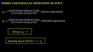


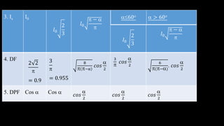
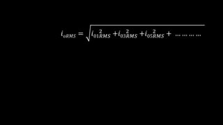
![Table – 1 [I0 constant]
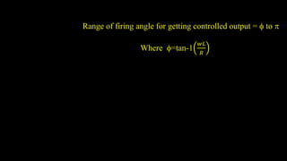
Where = 𝑇𝑎𝑛−1 𝑤𝐿
𝑅
1- full
convertor
3- full
converter
1- semi
converter
3- semi converter
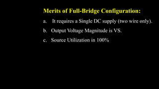
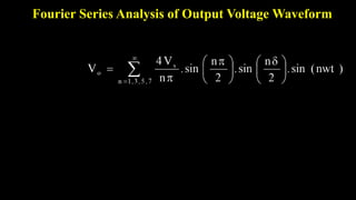
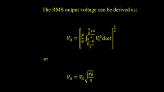
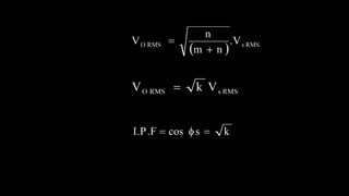
1. V0
2
𝑣𝑚
𝑐𝑜𝑠 3
𝑣𝑚𝑙
𝑐𝑜𝑠
𝑣𝑚
1 + 𝑐𝑜𝑠 𝑣0 = 3
𝑣𝑚𝑙
2
1 + 𝑐𝑜𝑠
𝐼𝑠1 =
6
𝐼0𝑐𝑜𝑠
2
2. 𝐼𝑠1
2 2
𝐼0
= 0.9𝐼0
8
𝐼0 = 0.9 𝐼0
2 2
𝐼0 𝑐𝑜𝑠
2
AC to DC Converters](https://image.slidesharecdn.com/ytlivetspscae-230320141126-d7f733c7/85/YT-Live-TSPSC-AE-pptx-127-320.jpg)


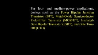
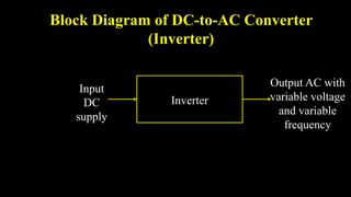
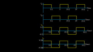
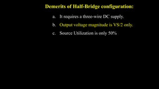
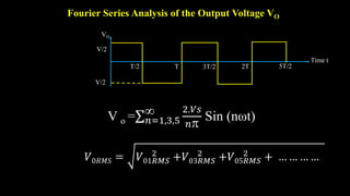
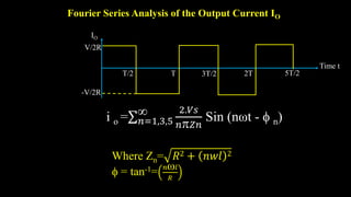
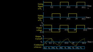
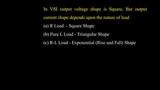
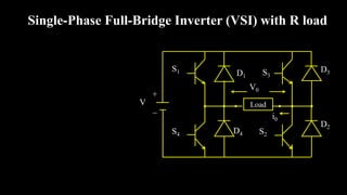
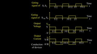

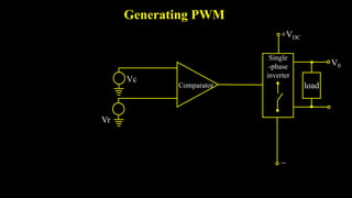
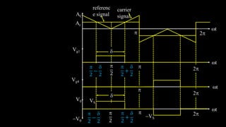


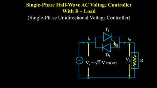
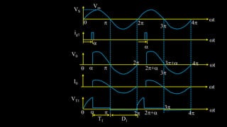
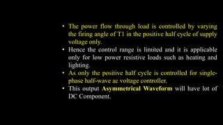
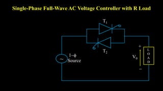


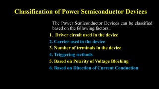
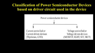
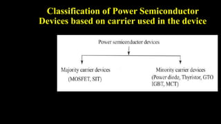
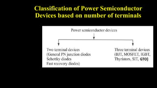
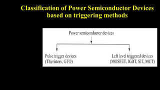
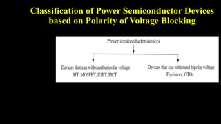
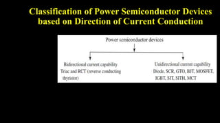
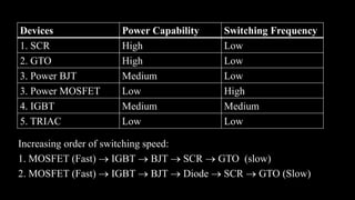
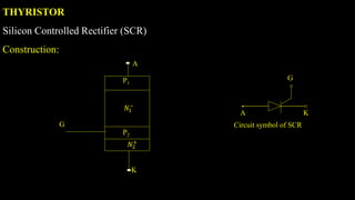
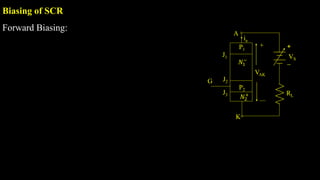
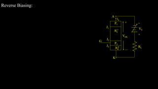
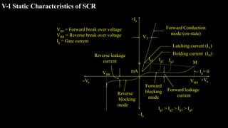
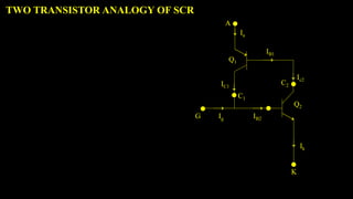
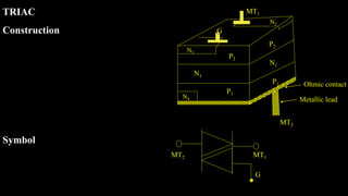
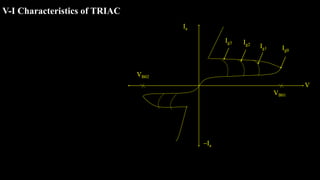
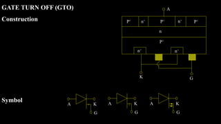
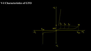
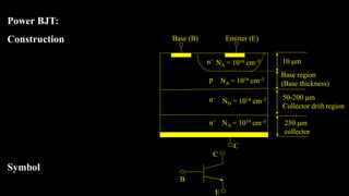
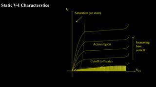
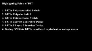
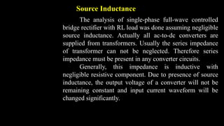
The document provides information on various power semiconductor devices. It begins by classifying power semiconductor devices based on different factors such as the driver circuit used, the carrier used, the number of terminals, triggering methods, polarity of voltage blocking, and direction of current conduction. It then provides details on specific devices such as thyristors (SCR), TRIACs, GTOs, power BJTs, IGBTs, power MOSFETs. It discusses the construction, working, characteristics and applications of these devices. It also provides comparisons between different devices in terms of switching speed and power capability. The document concludes by discussing AC to DC converters and rectifiers.


