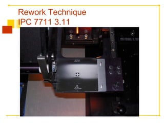
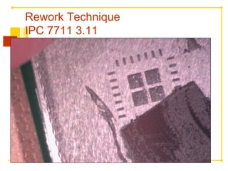
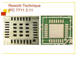
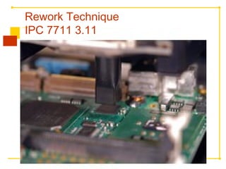
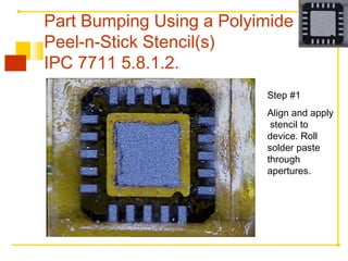
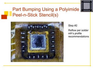
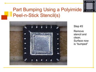
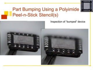
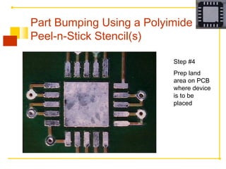
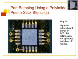
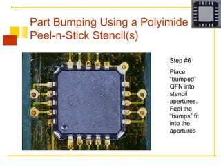
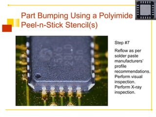
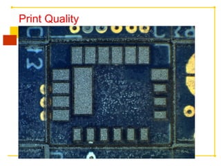
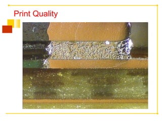
QFN Rework
A Primer
BEST Inc. www.solder.net
info@solder.net
Rework Technique
IPC 7711 3.11
Rework Technique
IPC 7711 3.11
Rework Technique
IPC 7711 3.11
Rework Technique
IPC 7711 3.11
Step #1
Align and apply
stencil to
device. Roll
solder paste
through
apertures.
Part Bumping Using a Polyimide
Peel-n-Stick Stencil(s)
IPC 7711 5.8.1.2.
Step #2
Reflow per solder
mfr’s profile
recommendations
Part Bumping Using a Polyimide
Peel-n-Stick Stencil(s)
Step #3
Remove
stencil and
clean.
Surface now
is “bumped”
Part Bumping Using a Polyimide
Peel-n-Stick Stencil(s)
Inspection of “bumped” device
Part Bumping Using a Polyimide
Peel-n-Stick Stencil(s)
Step #4
Prep land
area on PCB
where device
is to be
placed
Part Bumping Using a Polyimide
Peel-n-Stick Stencil(s)
Step #5
Align and
adhere board
stencil on
PCB. Roll
solder paste
into apertures
and clean off
residue.
Part Bumping Using a Polyimide
Peel-n-Stick Stencil(s)
Step #6
Place
“bumped”
QFN into
stencil
apertures.
Feel the
“bumps” fit
into the
apertures
Part Bumping Using a Polyimide
Peel-n-Stick Stencil(s)
Step #7
Reflow as per
solder paste
manufacturers’
profile
recommendations.
Perform visual
inspection.
Perform X-ray
inspection.
Part Bumping Using a Polyimide
Peel-n-Stick Stencil(s)
Print Quality
Print Quality
BEST Inc.
www.solder.net

QFN Rework

Editor's Notes

  • #2 Background 2006 RoHS Fast Forward we have more 0201s, stacked packages, leadless devices have replaced BGAs in terms of # of placements and lead free solder pastes are NOT going away # 2 is Novemeber 1 st from 1-2:30PM EST