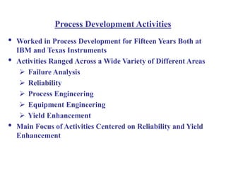
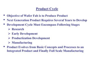
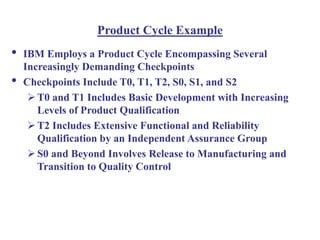
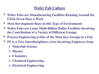
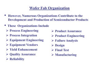
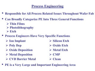
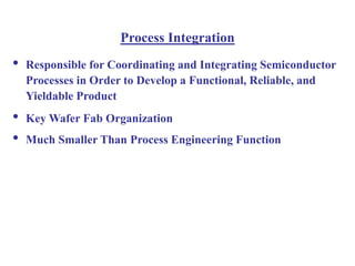
Process Development and Process
Integration of Semiconductor Devices
Mark T. Tinker, Ph.D.
Department of Electrical Engineering
University of Texas at Dallas
Process Development Activities
• Worked in Process Development for Fifteen Years Both at
IBM and Texas Instruments
• Activities Ranged Across a Wide Variety of Different Areas
 Failure Analysis
 Reliability
 Process Engineering
 Equipment Engineering
 Yield Enhancement
• Main Focus of Activities Centered on Reliability and Yield
Enhancement
Product Cycle
• Objective of Wafer Fab is to Produce Product
• Next Generation Product Requires Several Years to Develop
• Development Cycle Must Encompass Following Stages
 Research
 Early Development
 Productization Development
 Manufacturing
• Product Evolves from Basic Concepts and Processes to an
Integrated Product and Finally Full Scale Manufacturing
Product Cycle Example
• IBM Employs a Product Cycle Encompassing Several
Increasingly Demanding Checkpoints
• Checkpoints Include T0, T1, T2, S0, S1, and S2
T0 and T1 Includes Basic Development with Increasing
Levels of Product Qualification
T2 Includes Extensive Functional and Reliability
Qualification by an Independent Assurance Group
S0 and Beyond Involves Release to Manufacturing and
Transition to Quality Control
Wafer Fab Culture
• Wafer Fabs are Manufacturing Facilities Running Around the
Clock Seven Days a Week
• Most Development Runs in this Type of Environment
• Wafer Fabs are Large Multi-Billion Dollar Facilities Involving
the Contribution of a Variety of Different Groups
• Process Engineering is One of the Most Key Groups in a Fab
• PE is a Very Interdisciplinary Area Involving Engineers from
 Materials Science
 Physics
 Chemistry
 Chemical Engineering
 Electrical Engineering
Wafer Fab Organization
 Process Engineering
 Process Integration
 Equipment Engineering
 Equipment Vendors
 Yield Enhancement
 Quality Assurance
 Reliability
 Product Assurance
 Product Engineering
 Failure Analysis
 Design
 Final Test
 Manufacturing
• These Organizations Include
• However, Numerous Organizations Contribute to the
Development and Production of Semiconductor Products
Process Engineering
 Ion Implant
 Poly Dep
 Oxide Deposition
 Metal Deposition
 CVD Barrier Metal
 Silicon Etch
 Oxide Etch
 Metal Etch
 CMP
 Clean
• Responsible for All Process Related Issues Throughout Wafer Fab
• Can Broadly Categorize PE Into Three General Functions
 Thin Films
 Photolithography
 Etch
• Process Engineers Have Very Specific Functions
• PE is a Very Large and Important Engineering Area
Process Integration
• Responsible for Coordinating and Integrating Semiconductor
Processes in Order to Develop a Functional, Reliable, and
Yieldable Product
• Key Wafer Fab Organization
• Much Smaller Than Process Engineering Function
Equipment Engineering
• Sustains and Supports Manufacturing Equipment In-Line
• PE and EE Often Work Together on Resolving Tool Issues
• Responsible for Coordinating Tool Installs
• EE Oftentimes Works with PE on Evaluating and Accepting
Next Generation Tools
Equipment Vendors
• Develops Equipment for Semiconductor Manufacturing
Develops Tool Platform and Process for Manufacturing
PE May Alter or Adjust Process to Meet Manufacturing
Needs
• Often Supports and Maintains Their Equipment In-Line in
Place of EE Under Equipment Service Contract
Yield Enhancement
• Drives Product Yield In-Line In Order to Expedite Yield
Learning
Shorten Product Cycle During Product Development
Or Maximize Product Yield During Manufacturing
• Typically Uses Expensive Defect Detection Tools In-Line to
Identify Yield Limiting Problems
• Companies Like IBM Also Depend Heavily Upon In-Line
Parametrics on Test Sites to Drive Yield In-Line
• Problems May Range from Regular Daily Particle Excursions
to Large Catastrophic Yield Problems
Quality Assurance
• Sets Up Control Charts and Limits for Various Process
Parameters
• May Actively Monitor and Enforce Quality Standards
Reliability
• Assures and Monitors Product Reliability
Serious Reliability Issues Can Be Disastrous for a Company
Can Be Costly for a Company and Seriously Hurt Its
Reputation
Responding to a Reliability Problem in the Field Can Take
Months
• Main Responsibilities Include
Stressing Product During Product Qualification
Implementing In-Line Monitors and Controls
Monitoring Field Returns for Problems and Issues
Product Assurance
• Performs Qualification of Product Prior to Product Release
Extensive Reliability Test
Extensive Functionality Test
Assures Manufacturability of Product
• Performed by Independent Product Organization to Assure
Unbiased Assessment
Product Engineering
• Drives Yield from End of Line By
Evaluating End of Line Final Test Data and Parametrics
Performing Failure Analysis of Defective Product
• Provides a Powerful Combination of Electrical Data Analysis
with Physical Failure Analysis
• However, Issues Include
Long Turnaround Time Before Product Reaches Final Test
Extensive Time Required for Physical Failure Analysis
Failure Analysis
• Provides Physical Failure Analysis and Construction Analysis
for Various Engineering Functions Including
Process Engineering
Process Integration
Yield Enhancement
Reliability
Product Assurance
Product Engineering
• Provides
Basic Metallographic Services Such as Polishing and SEM
More Sophisticated Services Such as STEM, SIMS, Auger,
and ESCA
Design
• Design May Get Involved with Process Development Issues
Most Issues Are Typically Resolved Through a Process Action
However, Occasional Issues Must Be Resolved with a Design
Change
Final Test
• Develops Final Test for Semiconductor Product
• Provides Electrical Parametric Data Which Drives
Manufacturing Line
• Also, Provides Key Final Test Data Commonly Required to Fix
Product Yield
Manufacturing
• Actually Runs the Product Through the Manufacturing Line
• Large and Powerful Group Within a Wafer Fab
• Typically Engineering Teams Must Work Around
Manufacturing Even in Development in Order to
Minimize Turnaround Times and Maximize Yield Learning
in Development or
Minimize Turnaround Times and Improve Tool Utilization in
Manufacturing
Conclusions
• Process Development Very Long and Involved Engineering
Process
• Requires Numerous Groups to Develop and Yield a
Semiconductor Product

Process Development and Process Integration of Semiconductor Devices.ppt

  • 1.
    Process Development andProcess Integration of Semiconductor Devices Mark T. Tinker, Ph.D. Department of Electrical Engineering University of Texas at Dallas
  • 2.
    Process Development Activities •Worked in Process Development for Fifteen Years Both at IBM and Texas Instruments • Activities Ranged Across a Wide Variety of Different Areas  Failure Analysis  Reliability  Process Engineering  Equipment Engineering  Yield Enhancement • Main Focus of Activities Centered on Reliability and Yield Enhancement
  • 3.
    Product Cycle • Objectiveof Wafer Fab is to Produce Product • Next Generation Product Requires Several Years to Develop • Development Cycle Must Encompass Following Stages  Research  Early Development  Productization Development  Manufacturing • Product Evolves from Basic Concepts and Processes to an Integrated Product and Finally Full Scale Manufacturing
  • 4.
    Product Cycle Example •IBM Employs a Product Cycle Encompassing Several Increasingly Demanding Checkpoints • Checkpoints Include T0, T1, T2, S0, S1, and S2 T0 and T1 Includes Basic Development with Increasing Levels of Product Qualification T2 Includes Extensive Functional and Reliability Qualification by an Independent Assurance Group S0 and Beyond Involves Release to Manufacturing and Transition to Quality Control
  • 5.
    Wafer Fab Culture •Wafer Fabs are Manufacturing Facilities Running Around the Clock Seven Days a Week • Most Development Runs in this Type of Environment • Wafer Fabs are Large Multi-Billion Dollar Facilities Involving the Contribution of a Variety of Different Groups • Process Engineering is One of the Most Key Groups in a Fab • PE is a Very Interdisciplinary Area Involving Engineers from  Materials Science  Physics  Chemistry  Chemical Engineering  Electrical Engineering
  • 6.
    Wafer Fab Organization Process Engineering  Process Integration  Equipment Engineering  Equipment Vendors  Yield Enhancement  Quality Assurance  Reliability  Product Assurance  Product Engineering  Failure Analysis  Design  Final Test  Manufacturing • These Organizations Include • However, Numerous Organizations Contribute to the Development and Production of Semiconductor Products
  • 7.
    Process Engineering  IonImplant  Poly Dep  Oxide Deposition  Metal Deposition  CVD Barrier Metal  Silicon Etch  Oxide Etch  Metal Etch  CMP  Clean • Responsible for All Process Related Issues Throughout Wafer Fab • Can Broadly Categorize PE Into Three General Functions  Thin Films  Photolithography  Etch • Process Engineers Have Very Specific Functions • PE is a Very Large and Important Engineering Area
  • 8.
    Process Integration • Responsiblefor Coordinating and Integrating Semiconductor Processes in Order to Develop a Functional, Reliable, and Yieldable Product • Key Wafer Fab Organization • Much Smaller Than Process Engineering Function
  • 9.
    Equipment Engineering • Sustainsand Supports Manufacturing Equipment In-Line • PE and EE Often Work Together on Resolving Tool Issues • Responsible for Coordinating Tool Installs • EE Oftentimes Works with PE on Evaluating and Accepting Next Generation Tools
  • 10.
    Equipment Vendors • DevelopsEquipment for Semiconductor Manufacturing Develops Tool Platform and Process for Manufacturing PE May Alter or Adjust Process to Meet Manufacturing Needs • Often Supports and Maintains Their Equipment In-Line in Place of EE Under Equipment Service Contract
  • 11.
    Yield Enhancement • DrivesProduct Yield In-Line In Order to Expedite Yield Learning Shorten Product Cycle During Product Development Or Maximize Product Yield During Manufacturing • Typically Uses Expensive Defect Detection Tools In-Line to Identify Yield Limiting Problems • Companies Like IBM Also Depend Heavily Upon In-Line Parametrics on Test Sites to Drive Yield In-Line • Problems May Range from Regular Daily Particle Excursions to Large Catastrophic Yield Problems
  • 12.
    Quality Assurance • SetsUp Control Charts and Limits for Various Process Parameters • May Actively Monitor and Enforce Quality Standards
  • 13.
    Reliability • Assures andMonitors Product Reliability Serious Reliability Issues Can Be Disastrous for a Company Can Be Costly for a Company and Seriously Hurt Its Reputation Responding to a Reliability Problem in the Field Can Take Months • Main Responsibilities Include Stressing Product During Product Qualification Implementing In-Line Monitors and Controls Monitoring Field Returns for Problems and Issues
  • 14.
    Product Assurance • PerformsQualification of Product Prior to Product Release Extensive Reliability Test Extensive Functionality Test Assures Manufacturability of Product • Performed by Independent Product Organization to Assure Unbiased Assessment
  • 15.
    Product Engineering • DrivesYield from End of Line By Evaluating End of Line Final Test Data and Parametrics Performing Failure Analysis of Defective Product • Provides a Powerful Combination of Electrical Data Analysis with Physical Failure Analysis • However, Issues Include Long Turnaround Time Before Product Reaches Final Test Extensive Time Required for Physical Failure Analysis
  • 16.
    Failure Analysis • ProvidesPhysical Failure Analysis and Construction Analysis for Various Engineering Functions Including Process Engineering Process Integration Yield Enhancement Reliability Product Assurance Product Engineering • Provides Basic Metallographic Services Such as Polishing and SEM More Sophisticated Services Such as STEM, SIMS, Auger, and ESCA
  • 17.
    Design • Design MayGet Involved with Process Development Issues Most Issues Are Typically Resolved Through a Process Action However, Occasional Issues Must Be Resolved with a Design Change
  • 18.
    Final Test • DevelopsFinal Test for Semiconductor Product • Provides Electrical Parametric Data Which Drives Manufacturing Line • Also, Provides Key Final Test Data Commonly Required to Fix Product Yield
  • 19.
    Manufacturing • Actually Runsthe Product Through the Manufacturing Line • Large and Powerful Group Within a Wafer Fab • Typically Engineering Teams Must Work Around Manufacturing Even in Development in Order to Minimize Turnaround Times and Maximize Yield Learning in Development or Minimize Turnaround Times and Improve Tool Utilization in Manufacturing
  • 20.
    Conclusions • Process DevelopmentVery Long and Involved Engineering Process • Requires Numerous Groups to Develop and Yield a Semiconductor Product