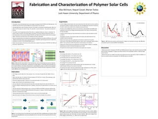
1. Fabrica on and Characteriza on of Polymer Solar Cells
Max McIntyre, Raquel Cossel, Marian Tzolov
Lock Haven University, Department of Physics
Results:
The average illuminated Voc of our devices was .25V.
The average illuminated Isc of our devices was 19.6μA.
The func onal area of our devices was 2.6x10‐5
m2
.
The average illuminated Jsc of our devices was .75A/m2
.
The average illuminated Pmax of our devices was .17W/m2
.
The average FF of our devices was .48.
The dielectric constant (k) of our devices polymer layer was calculated to be 5.15 a er
determining the thickness of our devices to be 46nm.
The photocurrent doesn’t decrease substan ally for light modulated up to 50 kHz, which
suggests that the life me of the photocurrent is less than 3 s.
Figure 4 : (A) Photocurrent spectrum with intensity in voltage, also converted to amps per wa . B) Op cal
transmission spectrum of the PCPBTDT and PCBM film.
Figure 3 : (A) Current‐voltage characteris cs under illumina on and dark condi ons. (B) Cur‐
rent‐voltage characteris cs under illumina on and dark condi ons in semi‐log scale. (C) Im‐
pedance spectroscopy under illumina on and dark condi ons. (D) Current‐voltage charac‐
teris c diagram showing how Isc, Voc, MPP, and FF are determined.
Introduc on:
The polymer solar cells fabricated had an ac ve region consis ng of both PCPBTBT and PCBM polymers. The
PCPDTBT acts as the donor and the PCBM acts as the acceptor in the solar cell.
Two electrodes were used in the device structure. The anode is a transparent conduc ng oxide, Indium Tin
Oxide. The ITO accepts the electron holes. The cathode is a strip of aluminum. The aluminum accepts the
electron.
The polymer solar cell generates photocurrent when it is exposed to light and a photon is absorbed. The
photon creates an exciton in the ac ve region of the device. The exciton diffuses toward the junc on. It
then disassociates at the interface between PCPDTBT and PCBM and the electron moves into the acceptor
PCBM. The electron and hole move to the cathode and anode, respec vely.
Electrical characteriza on of the devices were preformed to determine its quality and efficiency. The current
‐voltage characteris cs were used to calculate fill factors. Impedance spectroscopy was done to determine
the dielectric constant of the PCPDTBT/PCBM mixture.
Op cal characteriza on of the devices were preformed to evaluate the presence of PCPDTBT and PCBM and
the devices’ response me.
Fabrica on:
Cut ITO glass covered slides into 2.54cm squares. Put a 1.3cm piece of tape down the middle of the cut
slides.
Pa ern the slide with a 3:1 solu on of HCl:H2O heated to 55°C‐60°C for 1 minute. Then submerge in two
separate water baths for 30 seconds each.
Sonicate the pa erned slides in Acetone, IPA, and deionized water for 15 minutes each.
Oxygen plasma treatment for approximately a minute.
Coat each slide with a filtered hole injec on layer (HIL) using sta c dispense then spin the slides for 10
seconds at 400rpm followed by 40 seconds at 1,200rpm. Anneal the HIL coated slides for 15 minutes each at
170°C.
Coat each slide with a filtered polymer that is a mixture of PCBM and PCPDTBT using sta c dispense then
spin the slides for 10 seconds at 400rpm followed by 40 seconds at 1,200rpm. Anneal the polymer coated
slides for 15 minutes each at 100°C.
Thermal evaporate aluminum strips that are 2.54cm x 0.2cm on to the annealed slides.
Apply silver paste to the edges of the aluminum strips to increase the strength of the contacts.
Experiment:
Current‐Voltage characteriza on tests were preformed under illuminated and dark condi ons.
Illuminated condi ons included a fully lite room and a flashlight beam directed on the device.
The dark condi on was a black cloth completely covering the device.
The open circuit voltage (Voc), short circuit current (Isc), and max power point (MPP) were
obtained from the current‐voltage characteriza on data for each device, and the fill factor
(FF) was calculated.
Impedance spectroscopy tests were preformed for each device under illuminated and dark
condi ons.
The dielectric constant of the polymer region of the devices was determined from the
impedance spectroscopy data.
Op cal transmission tests were performed on the devices to determine the op cal
transmission of the PCBM and PCPDTBT polymer mixture, with a wavelength range of 300nm‐
900nm. This was done to confirm the presence of each polymer in the devices.
Photocurrent measurements were performed in the spectral 300nm‐1,000nm. A calibrated
photodiode was used to normalize the photocurrent to A/W.
The op cal transmission graph and the photocurrent graph were compared. Discussion:
‐ Op cal transmission: the polymer PCPDTBT and PCBM are present. Figure 4 (B) shows the presence of PCBM
with the 350nm wavelength. The figure also shows PCPDTBT at the wavelength of 800nm. PCBM has larger
volume frac on
‐ Photocurrent spectrum: Reflects the bands of the op cal transmission with peaks at 350nm and 800nm. Ex‐
citons are equally created and separated in the PCPDTBT polymer and PCBM.
Figure 2: Cross‐sec onal view of the fabrica on process steps. a) ITO glass slide b) pa erned ITO glass slide c)
HIL layer spincoa ng d) polymer layer spincoa ng e) aluminum strip layer thermal evapora on f) silver paste
contact points.
Figure 1: (A) Schema c representa on of bulk heterojunc on solar cell illustra ng the processes of light ab‐
sorp on and photocurrent genera on, supported by an energy diagram. (i) absorbed photon generates exci‐
ton. (ii) exciton diffusion. (iii) exciton disassocia on in electronega ve acceptor. (iv) electron‐hole separa on
due to electric field and material. (v) electron and hole move to cathode and anode, respec vely. (vi) photo‐
current. (B) Top view of complete device.