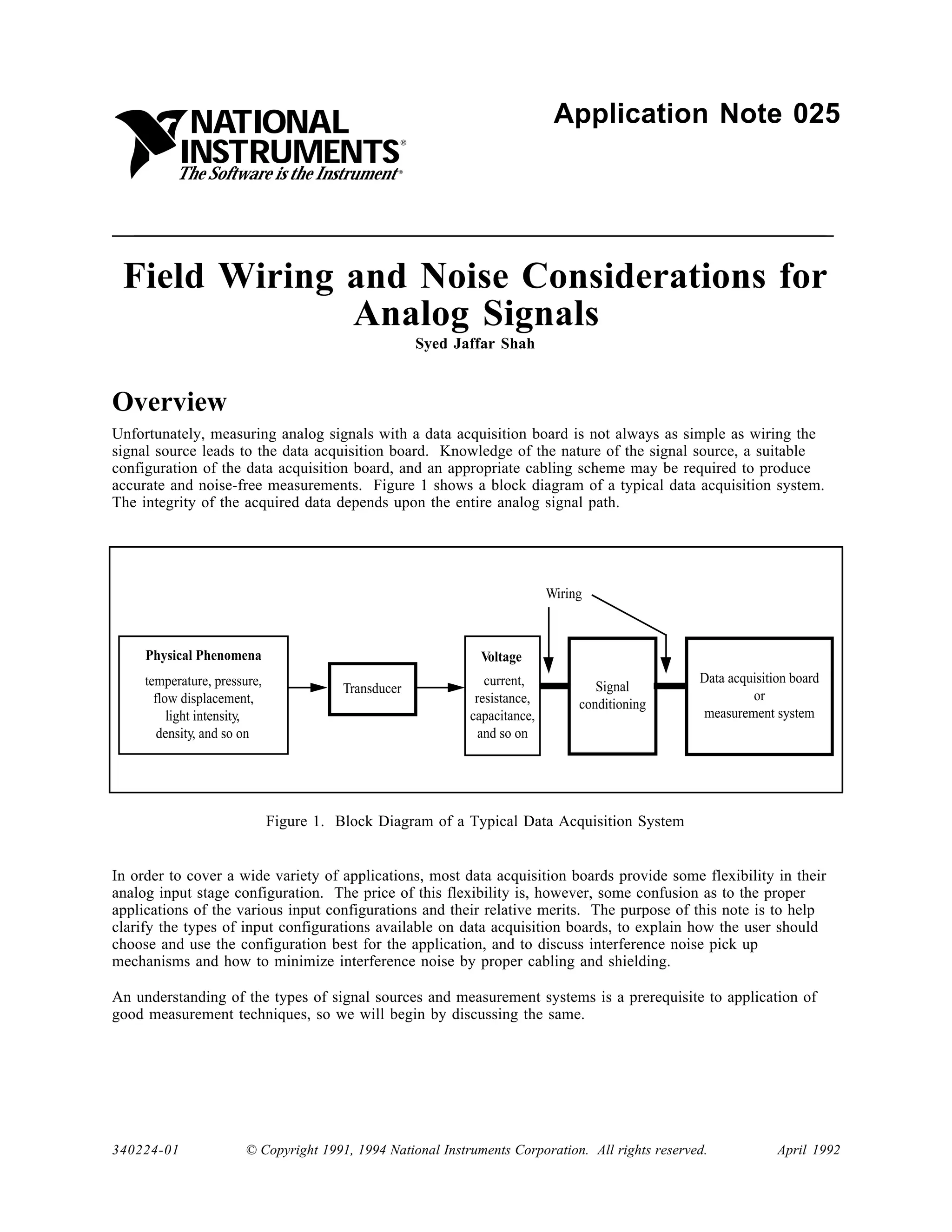
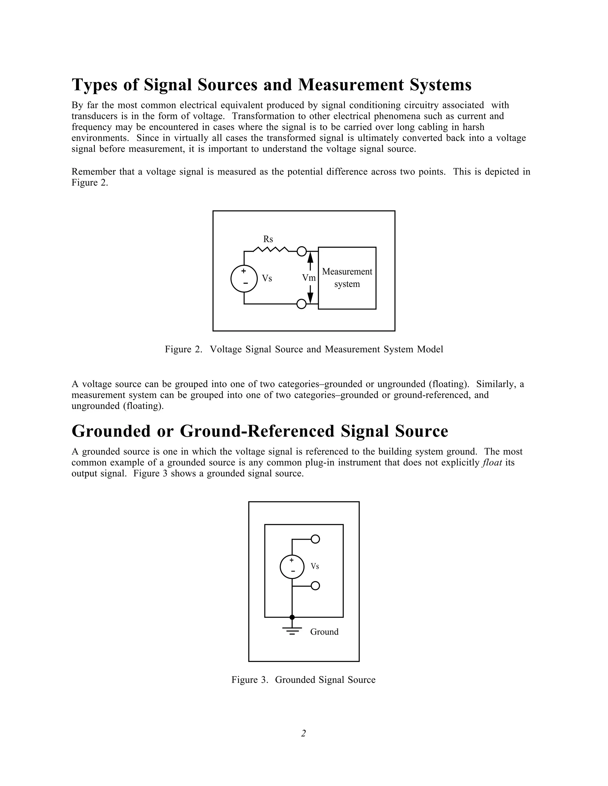
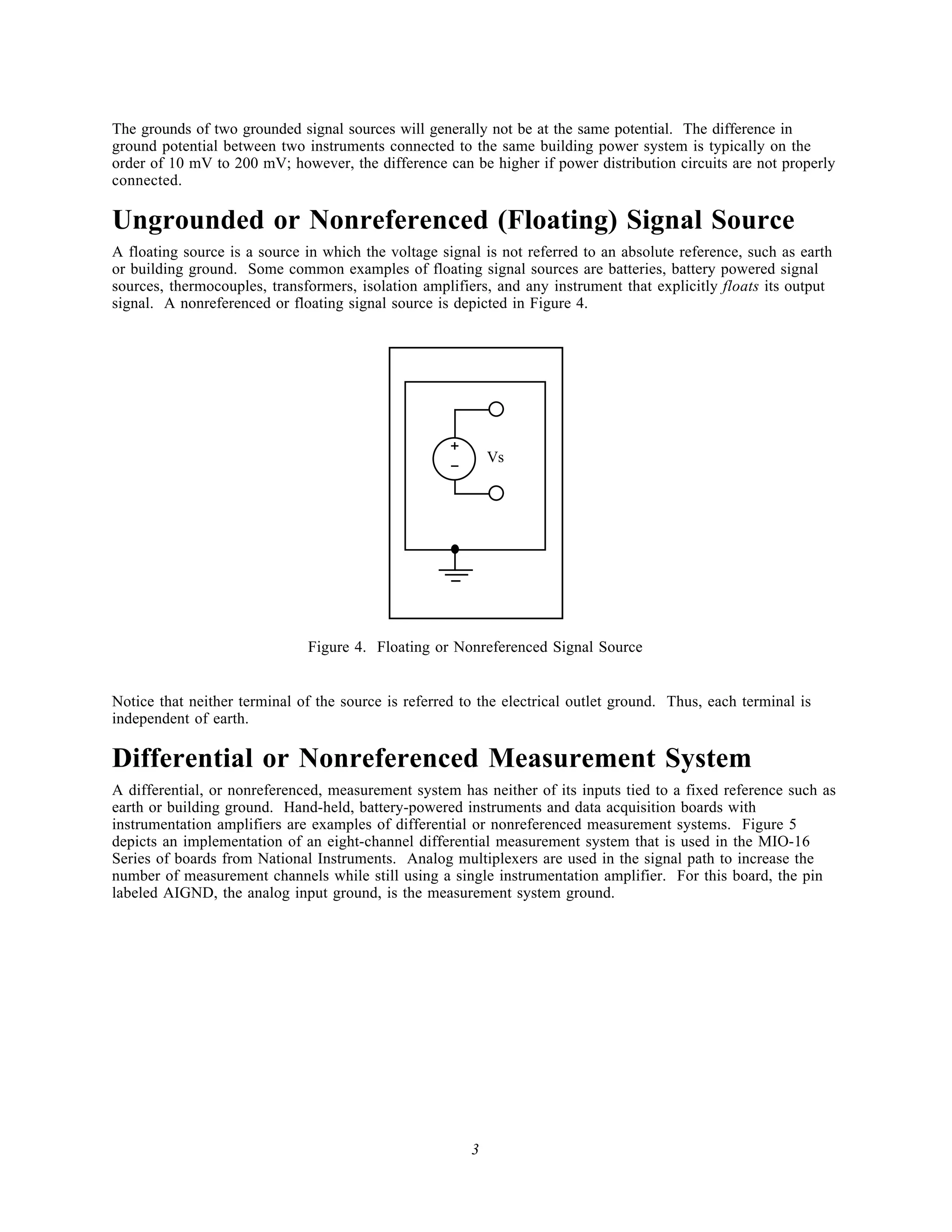
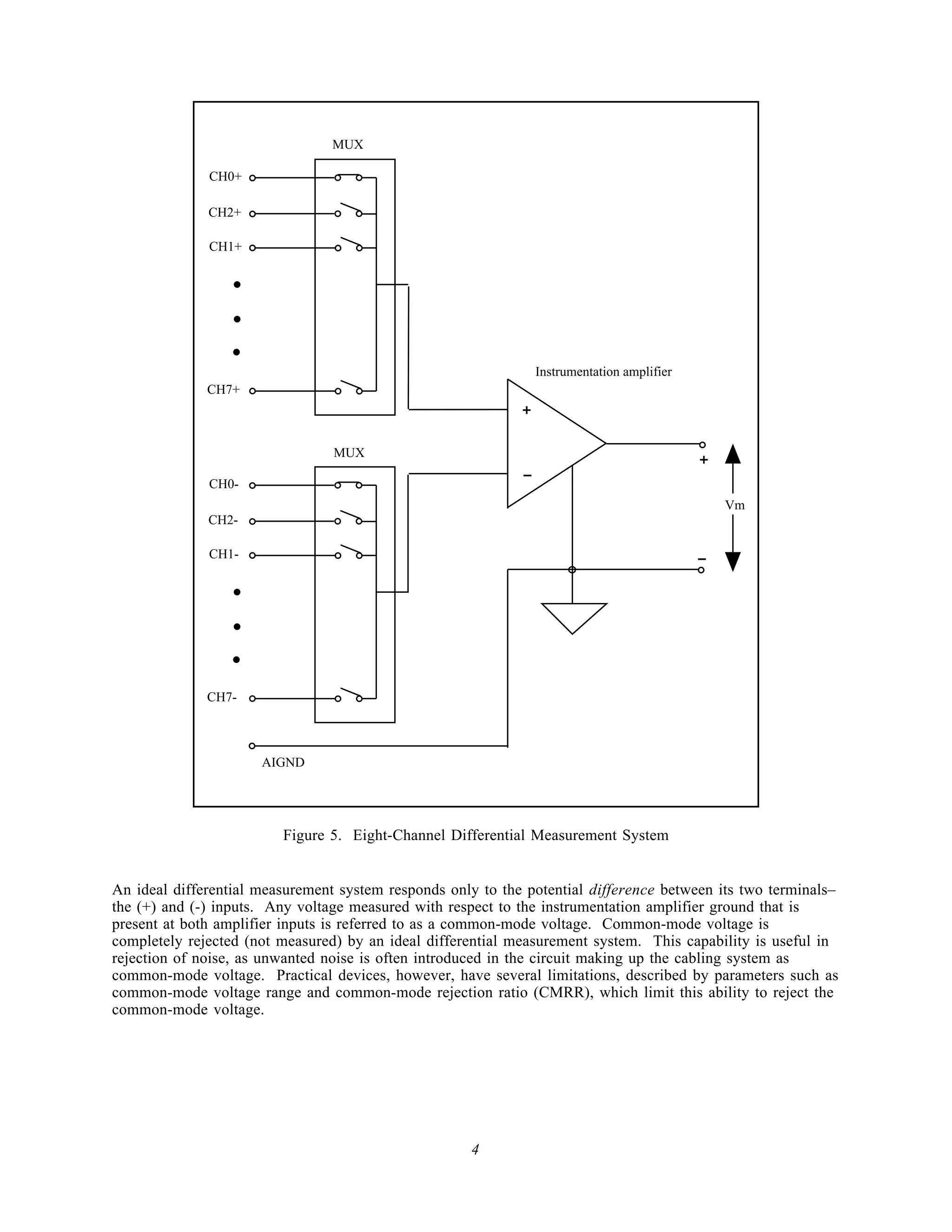
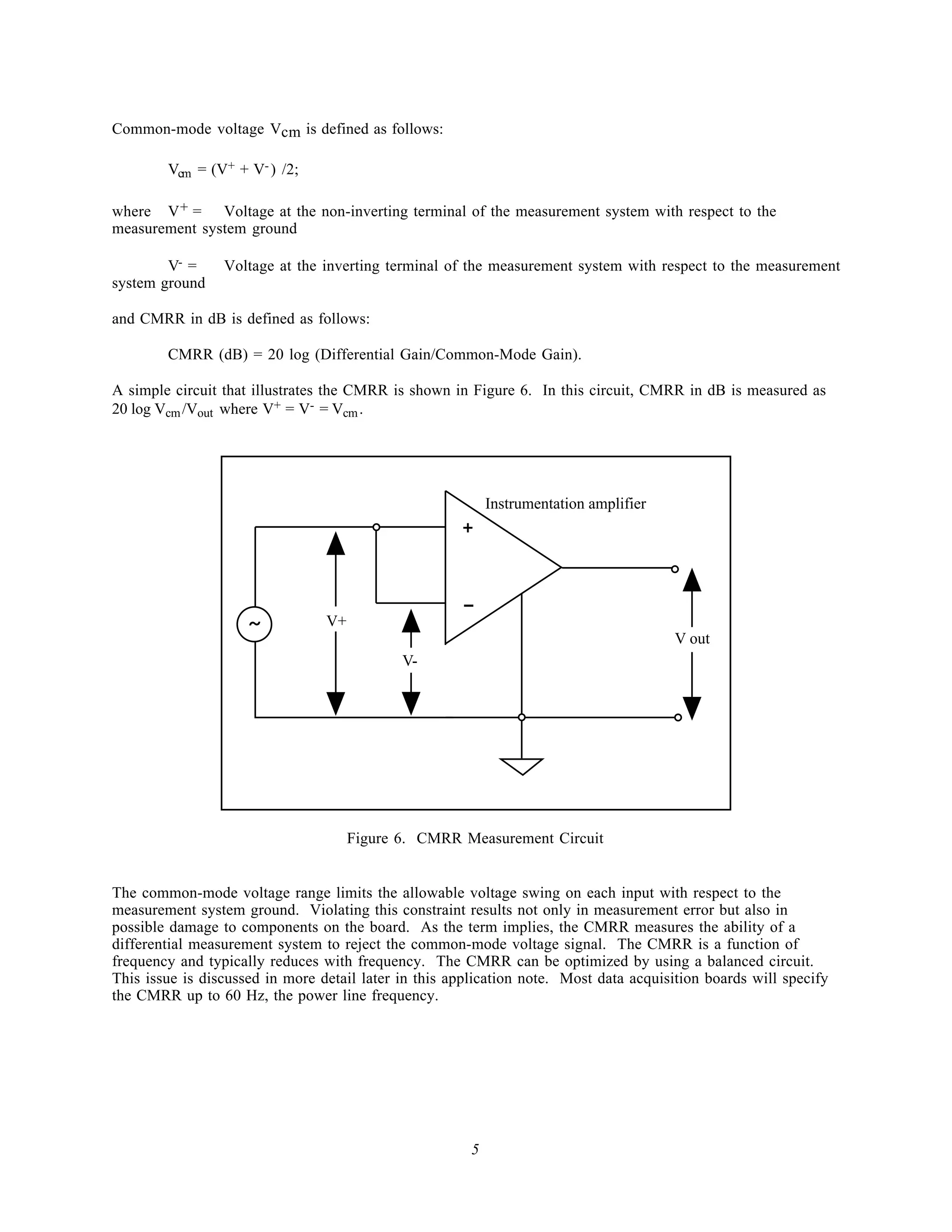
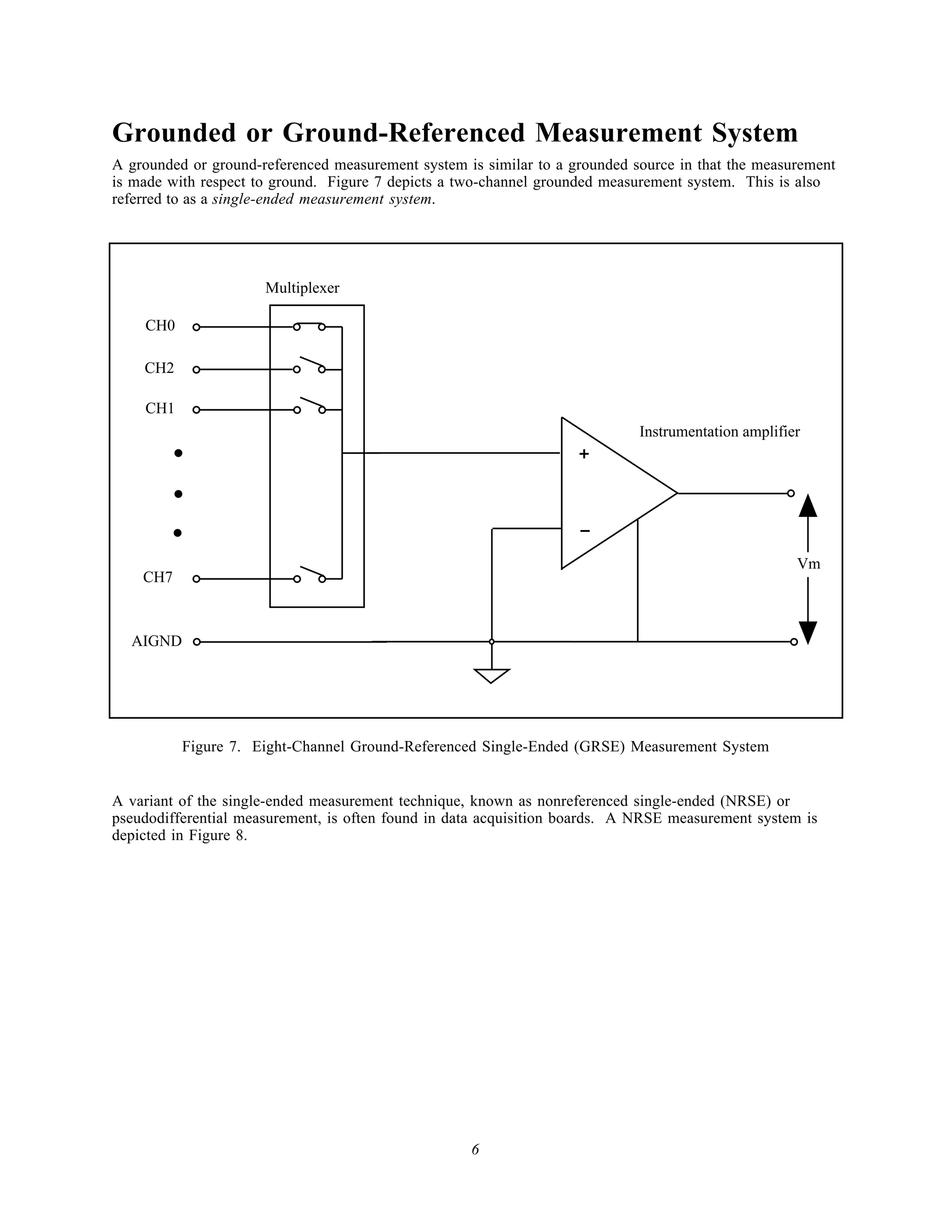
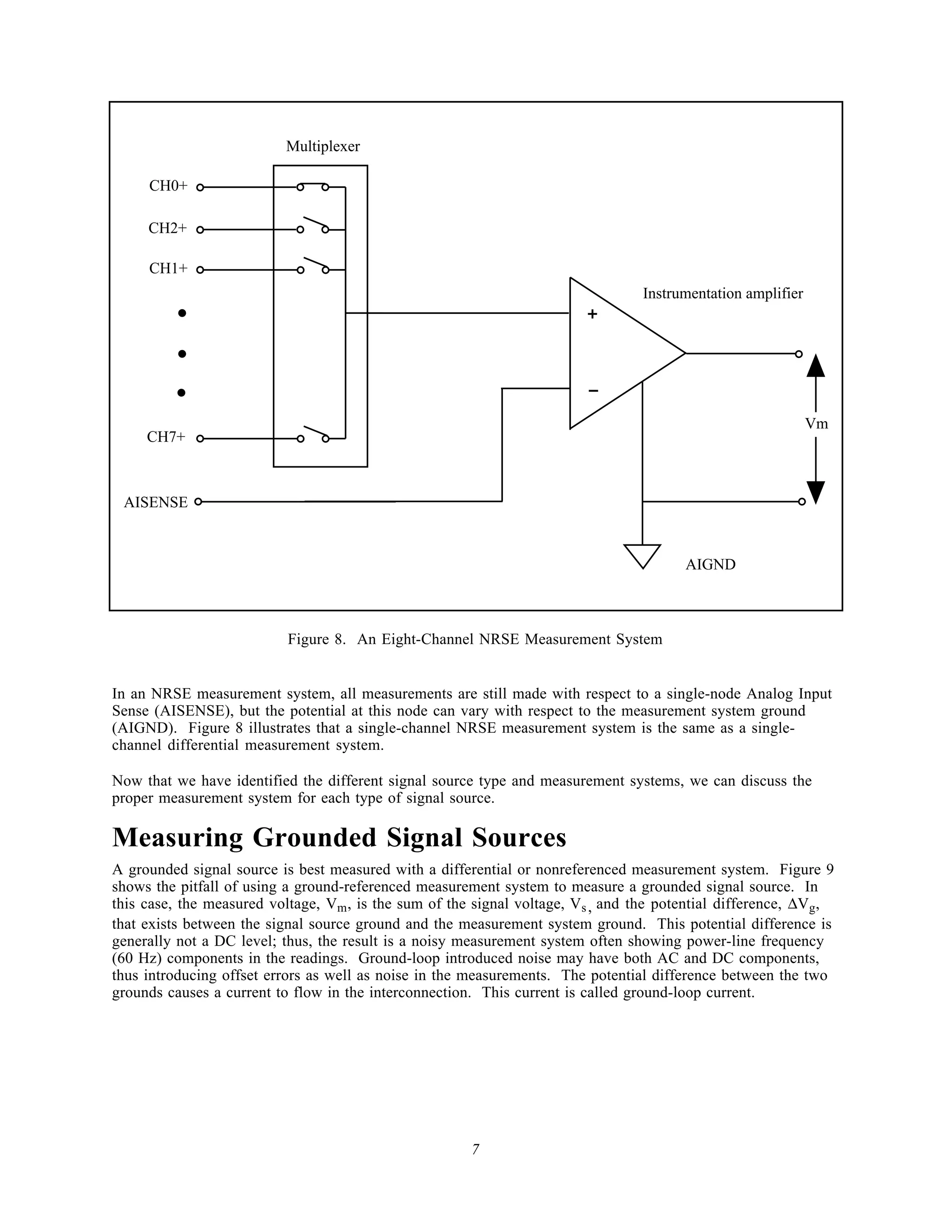
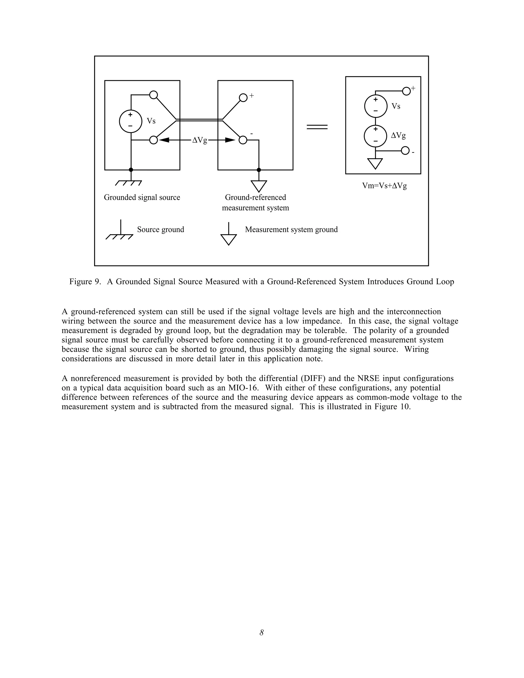
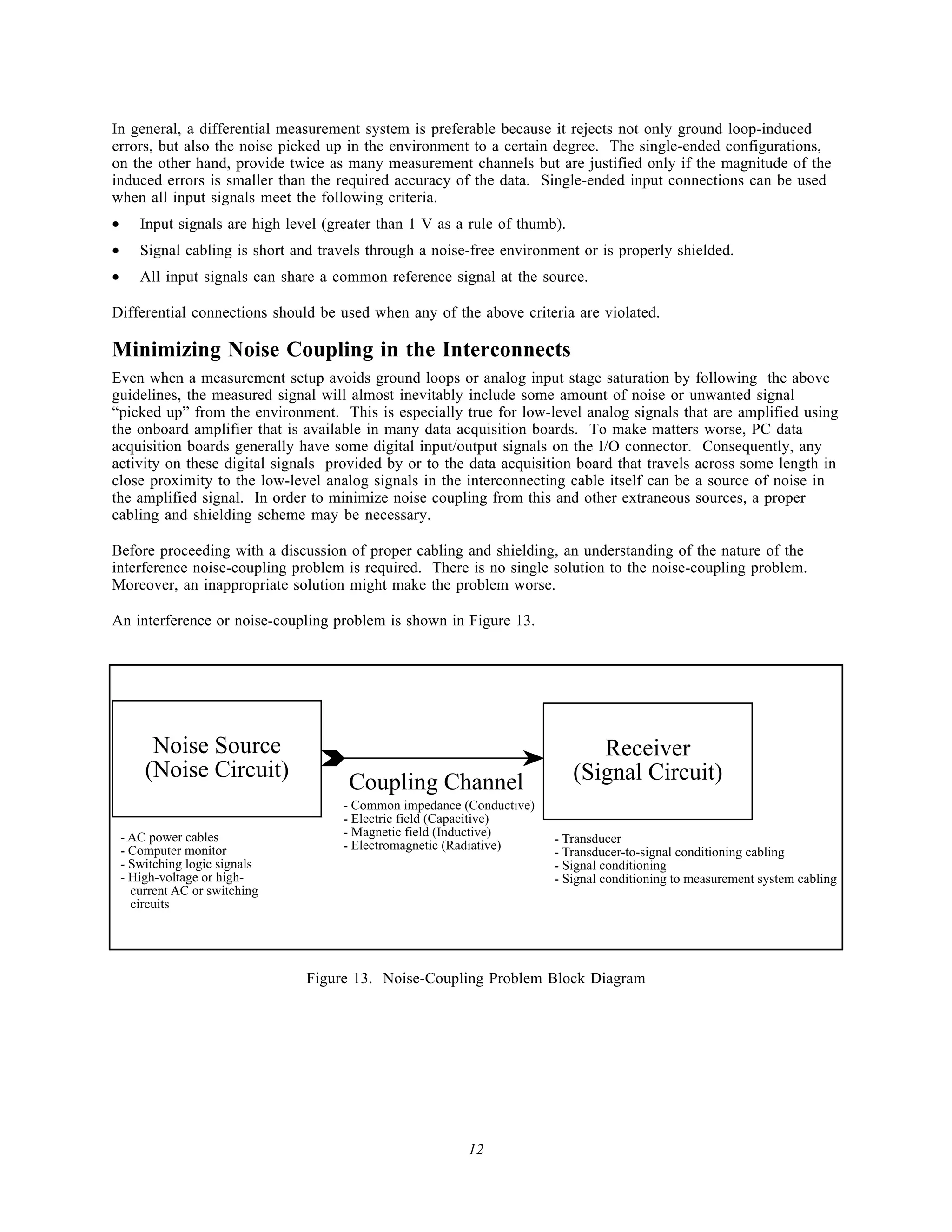
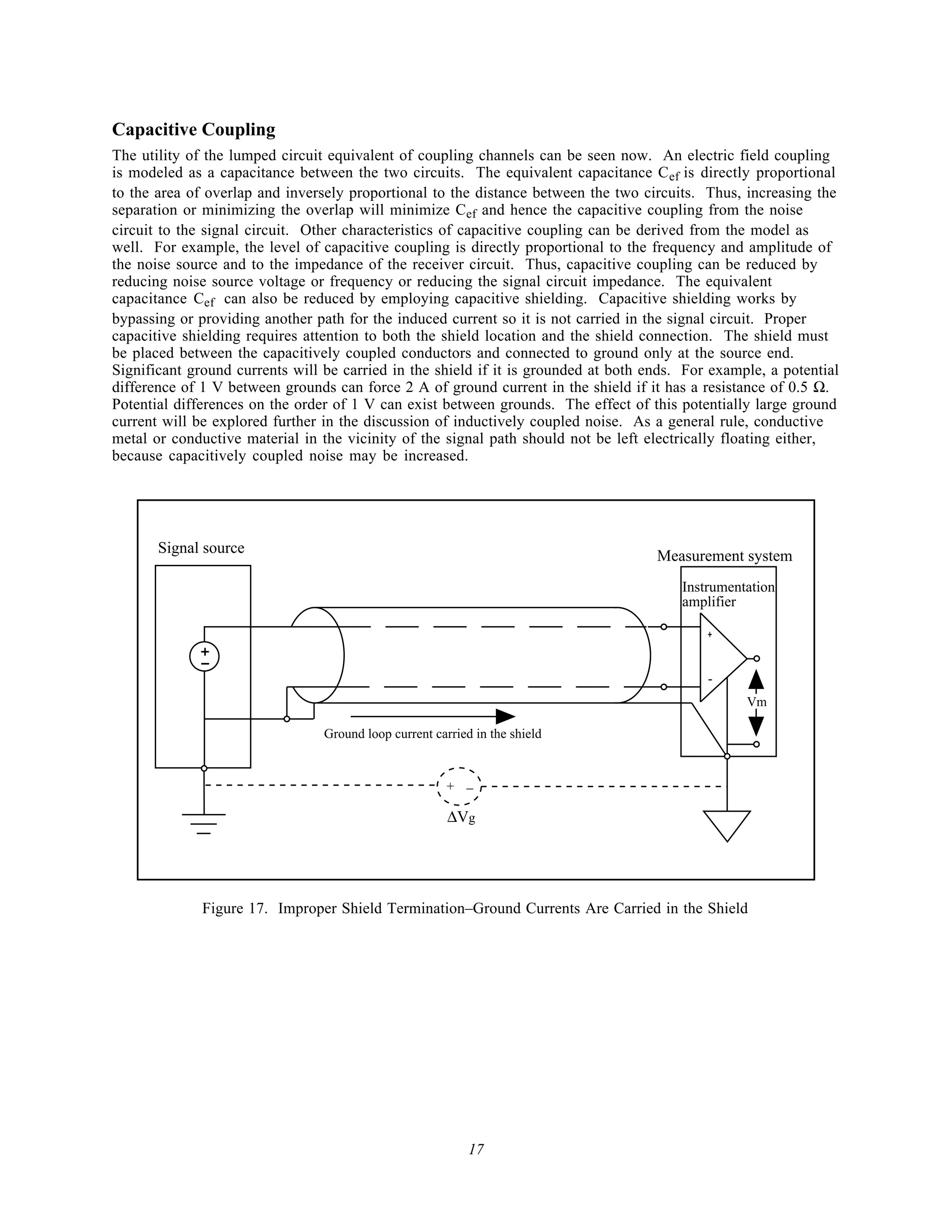
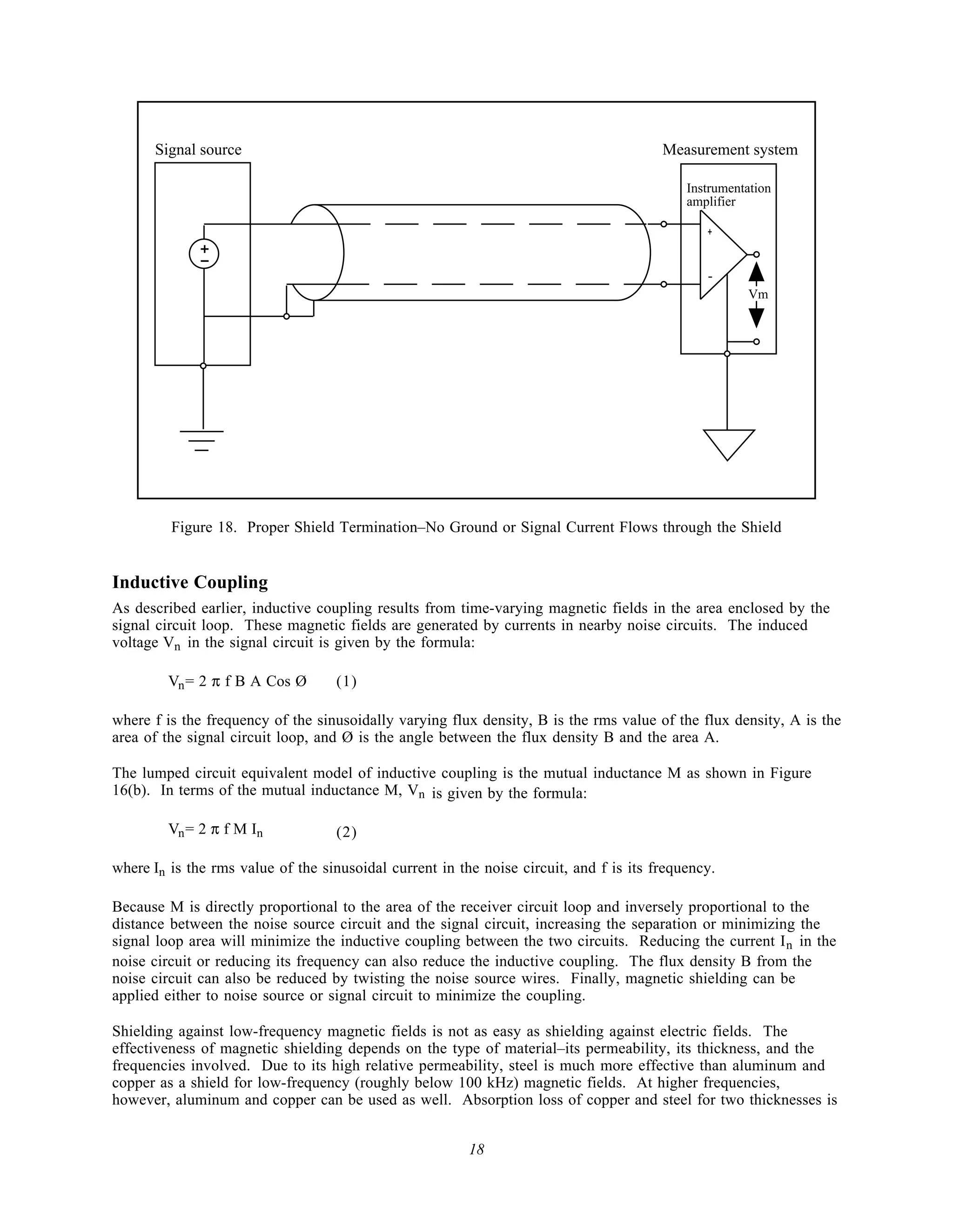
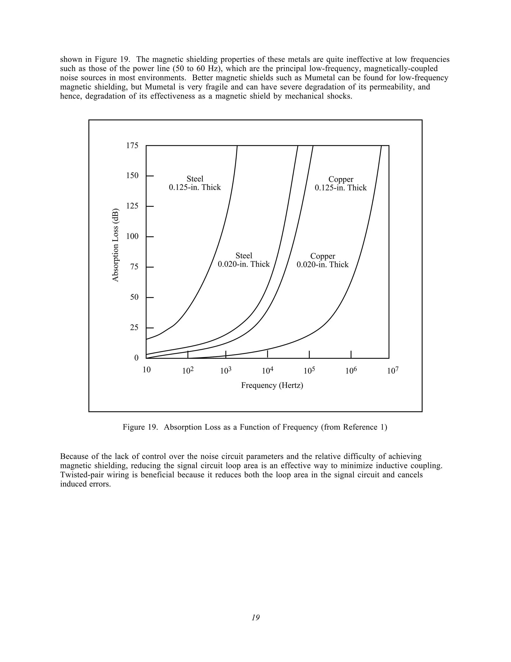
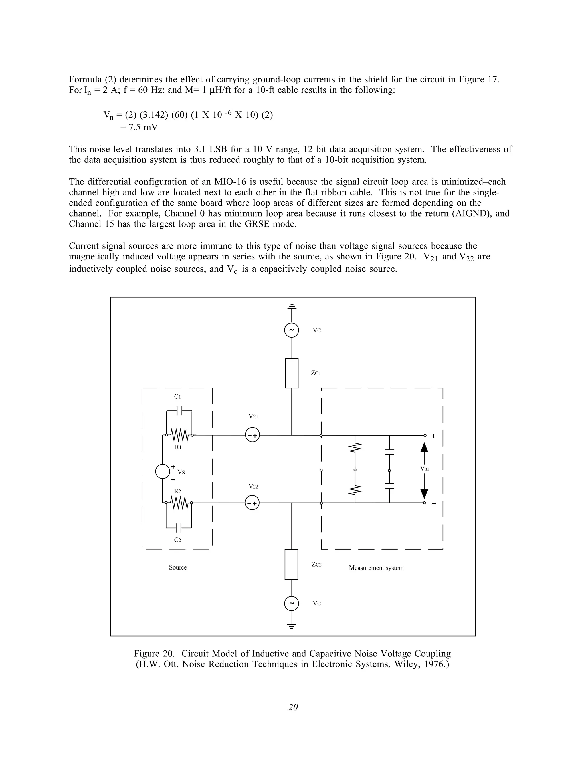
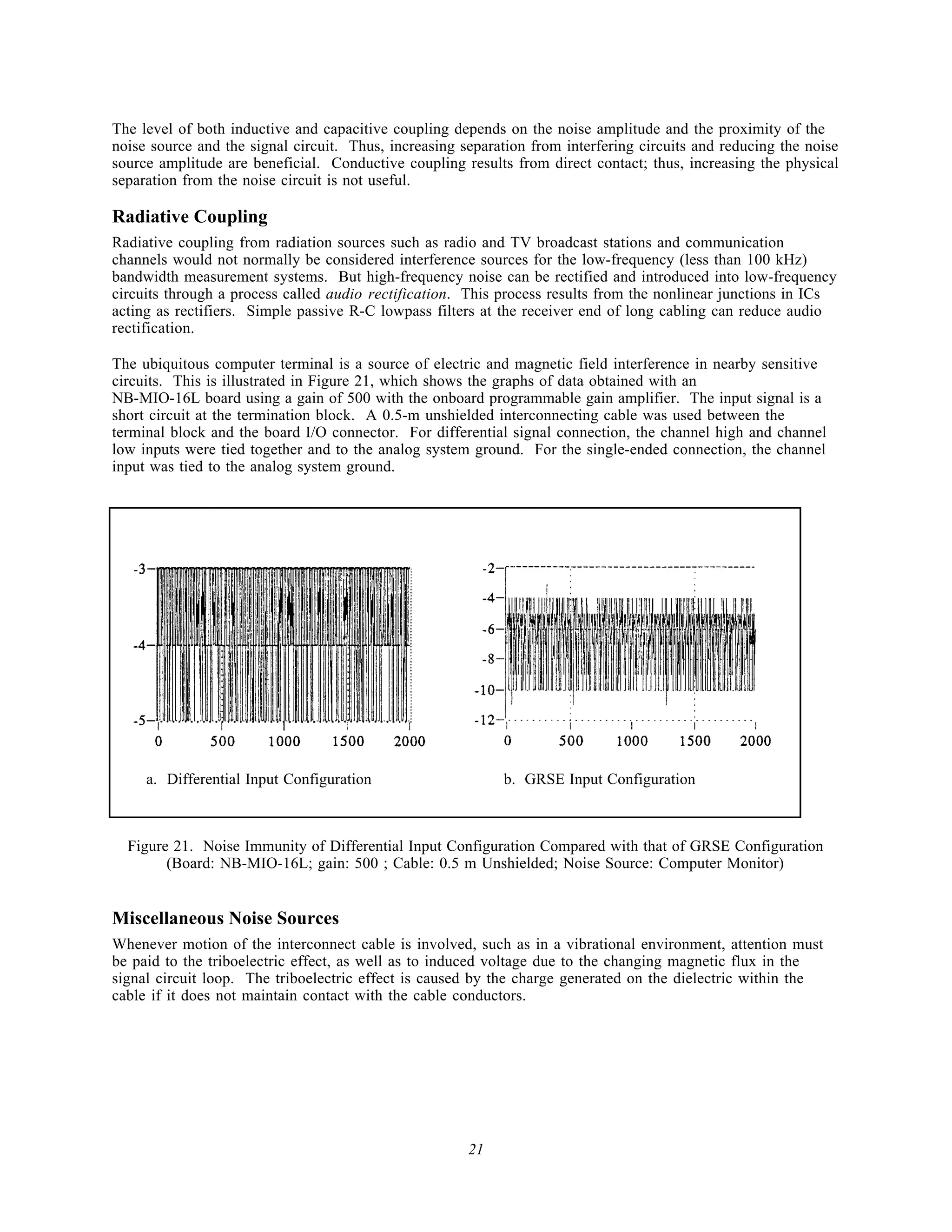
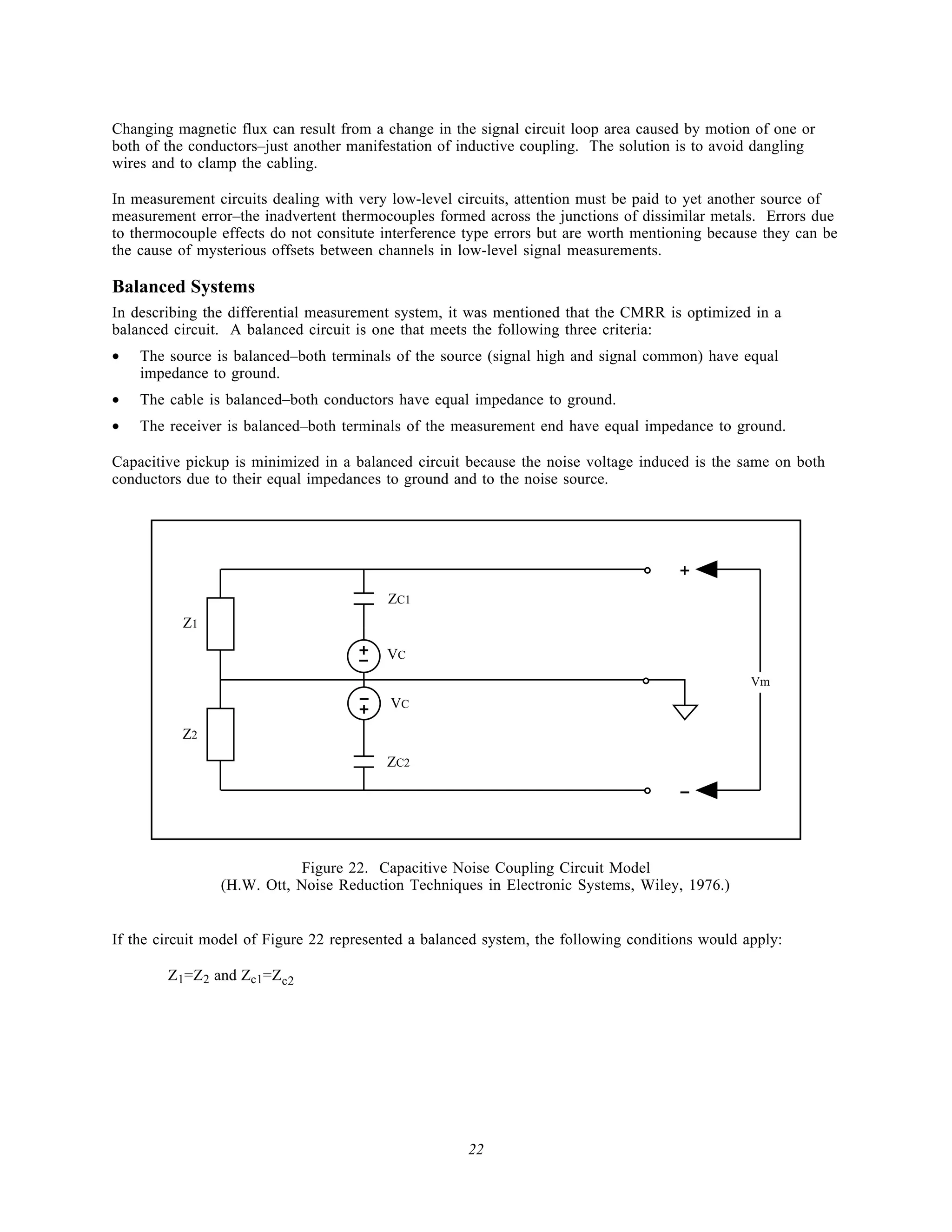
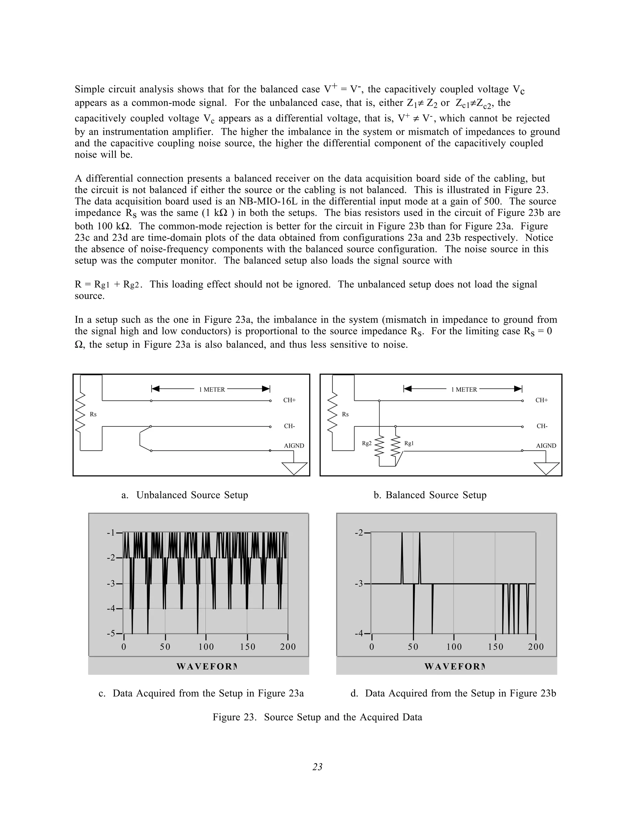
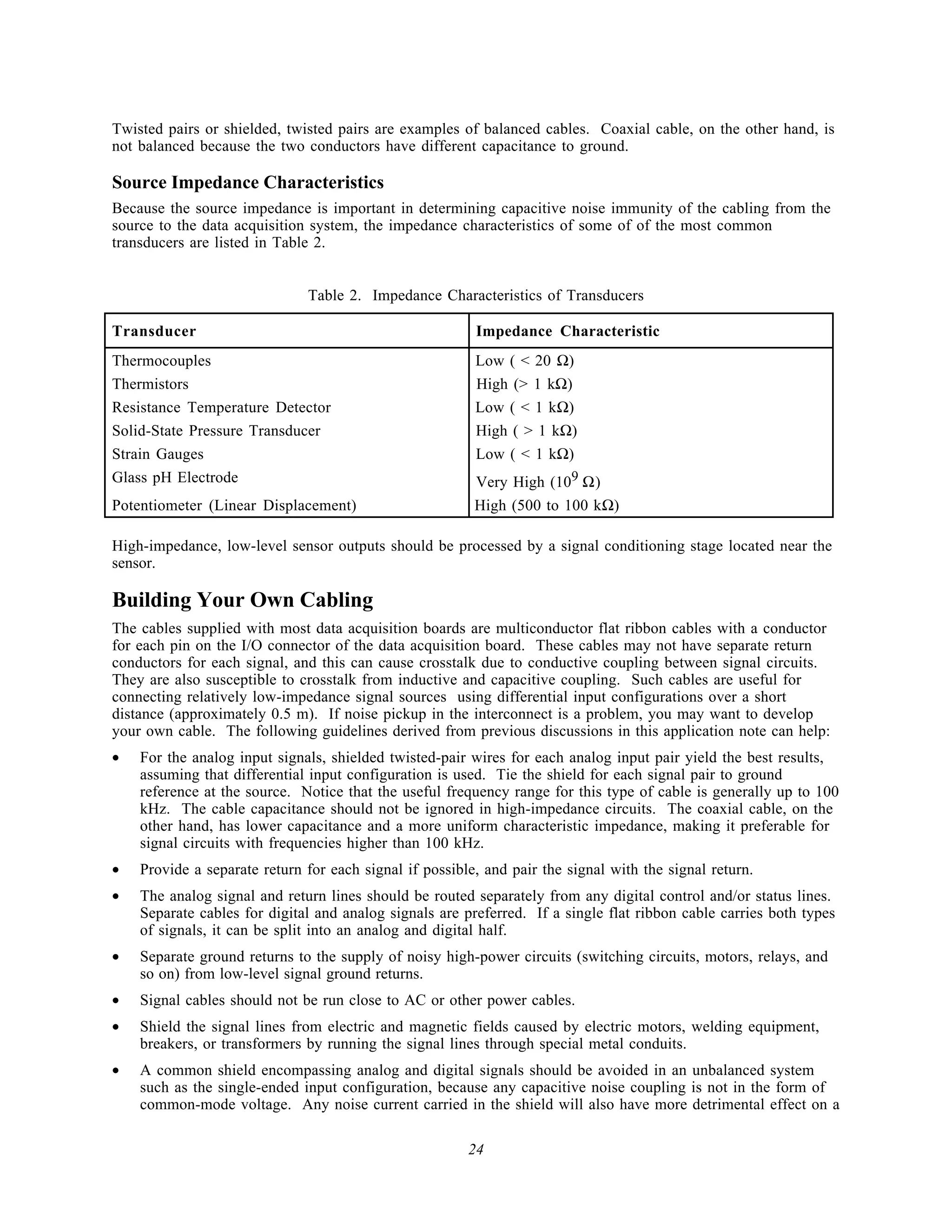
SlideShare a Scribd company logo
1 of 27
Download to read offline
NATIONAL                                                        Application Note 025
            INSTRUMENTS
                                                  ®


          The Software is the Instrument          ®


 Field Wiring and Noise Considerations for
              Analog Signals
                                                      Syed Jaffar Shah


Overview
Unfortunately, measuring analog signals with a data acquisition board is not always as simple as wiring the
signal source leads to the data acquisition board. Knowledge of the nature of the signal source, a suitable
configuration of the data acquisition board, and an appropriate cabling scheme may be required to produce
accurate and noise-free measurements. Figure 1 shows a block diagram of a typical data acquisition system.
The integrity of the acquired data depends upon the entire analog signal path.


                                                                            Wiring


     Physical Phenomena                                        Voltage
     temperature, pressure,                                     current,                          Data acquisition board
                                         Transducer                                 Signal
       flow displacement,                                     resistance,                                  or
                                                                                 conditioning
          light intensity,                                   capacitance,                         measurement system
        density, and so on                                     and so on


                              Figure 1. Block Diagram of a Typical Data Acquisition System


In order to cover a wide variety of applications, most data acquisition boards provide some flexibility in their
analog input stage configuration. The price of this flexibility is, however, some confusion as to the proper
applications of the various input configurations and their relative merits. The purpose of this note is to help
clarify the types of input configurations available on data acquisition boards, to explain how the user should
choose and use the configuration best for the application, and to discuss interference noise pick up
mechanisms and how to minimize interference noise by proper cabling and shielding.

An understanding of the types of signal sources and measurement systems is a prerequisite to application of
good measurement techniques, so we will begin by discussing the same.


340224-01              © Copyright 1991, 1994 National Instruments Corporation. All rights reserved.            April 1992
Types of Signal Sources and Measurement Systems
By far the most common electrical equivalent produced by signal conditioning circuitry associated with
transducers is in the form of voltage. Transformation to other electrical phenomena such as current and
frequency may be encountered in cases where the signal is to be carried over long cabling in harsh
environments. Since in virtually all cases the transformed signal is ultimately converted back into a voltage
signal before measurement, it is important to understand the voltage signal source.

Remember that a voltage signal is measured as the potential difference across two points. This is depicted in
Figure 2.


                                              Rs


                                        +               Vm
                                                                 Measurement
                                        -    Vs
                                                                   system


                      Figure 2. Voltage Signal Source and Measurement System Model


A voltage source can be grouped into one of two categories–grounded or ungrounded (floating). Similarly, a
measurement system can be grouped into one of two categories–grounded or ground-referenced, and
ungrounded (floating).

Grounded or Ground-Referenced Signal Source
A grounded source is one in which the voltage signal is referenced to the building system ground. The most
common example of a grounded source is any common plug-in instrument that does not explicitly float its
output signal. Figure 3 shows a grounded signal source.


                                                    +       Vs
                                                    -


                                                            Ground


                                      Figure 3. Grounded Signal Source


                                                        2
The grounds of two grounded signal sources will generally not be at the same potential. The difference in
ground potential between two instruments connected to the same building power system is typically on the
order of 10 mV to 200 mV; however, the difference can be higher if power distribution circuits are not properly
connected.

Ungrounded or Nonreferenced (Floating) Signal Source
A floating source is a source in which the voltage signal is not referred to an absolute reference, such as earth
or building ground. Some common examples of floating signal sources are batteries, battery powered signal
sources, thermocouples, transformers, isolation amplifiers, and any instrument that explicitly floats its output
signal. A nonreferenced or floating signal source is depicted in Figure 4.


                                                     +       Vs
                                                     -


                                                    Fl   i


                              Figure 4. Floating or Nonreferenced Signal Source


Notice that neither terminal of the source is referred to the electrical outlet ground. Thus, each terminal is
independent of earth.

Differential or Nonreferenced Measurement System
A differential, or nonreferenced, measurement system has neither of its inputs tied to a fixed reference such as
earth or building ground. Hand-held, battery-powered instruments and data acquisition boards with
instrumentation amplifiers are examples of differential or nonreferenced measurement systems. Figure 5
depicts an implementation of an eight-channel differential measurement system that is used in the MIO-16
Series of boards from National Instruments. Analog multiplexers are used in the signal path to increase the
number of measurement channels while still using a single instrumentation amplifier. For this board, the pin
labeled AIGND, the analog input ground, is the measurement system ground.


                                                         3
MUX

              CH0+

              CH2+

              CH1+


                                                                 Instrumentation amplifier
              CH7+
                                                             +

                                 MUX
                                                                                             +
              CH0-
                                                             -
                                                                                                 Vm
              CH2-

              CH1-                                                                           -


              CH7-


                      AIGND


                         Figure 5. Eight-Channel Differential Measurement System


An ideal differential measurement system responds only to the potential difference between its two terminals–
the (+) and (-) inputs. Any voltage measured with respect to the instrumentation amplifier ground that is
present at both amplifier inputs is referred to as a common-mode voltage. Common-mode voltage is
completely rejected (not measured) by an ideal differential measurement system. This capability is useful in
rejection of noise, as unwanted noise is often introduced in the circuit making up the cabling system as
common-mode voltage. Practical devices, however, have several limitations, described by parameters such as
common-mode voltage range and common-mode rejection ratio (CMRR), which limit this ability to reject the
common-mode voltage.


                                                     4
Common-mode voltage Vcm is defined as follows:

        Vcm = (V+ + V- ) /2;

where V + = Voltage at the non-inverting terminal of the measurement system with respect to the
measurement system ground

        V- =     Voltage at the inverting terminal of the measurement system with respect to the measurement
system ground

and CMRR in dB is defined as follows:

        CMRR (dB) = 20 log (Differential Gain/Common-Mode Gain).

A simple circuit that illustrates the CMRR is shown in Figure 6. In this circuit, CMRR in dB is measured as
20 log Vcm /Vout where V+ = V- = Vcm .


                                                            Instrumentation amplifier
                                                      +


                                                      -
                     ~           V+
                                                                                        V out
                                             V-


                                      Figure 6. CMRR Measurement Circuit


The common-mode voltage range limits the allowable voltage swing on each input with respect to the
measurement system ground. Violating this constraint results not only in measurement error but also in
possible damage to components on the board. As the term implies, the CMRR measures the ability of a
differential measurement system to reject the common-mode voltage signal. The CMRR is a function of
frequency and typically reduces with frequency. The CMRR can be optimized by using a balanced circuit.
This issue is discussed in more detail later in this application note. Most data acquisition boards will specify
the CMRR up to 60 Hz, the power line frequency.


                                                        5
Grounded or Ground-Referenced Measurement System
A grounded or ground-referenced measurement system is similar to a grounded source in that the measurement
is made with respect to ground. Figure 7 depicts a two-channel grounded measurement system. This is also
referred to as a single-ended measurement system.


                      Multiplexer

    CH0

    CH2

    CH1
                                                                             Instrumentation amplifier
                                                                    +


                                                                    -
                                                                                                     Vm
    CH7


  AIGND


          Figure 7. Eight-Channel Ground-Referenced Single-Ended (GRSE) Measurement System


A variant of the single-ended measurement technique, known as nonreferenced single-ended (NRSE) or
pseudodifferential measurement, is often found in data acquisition boards. A NRSE measurement system is
depicted in Figure 8.


                                                    6
Multiplexer

     CH0+

     CH2+

     CH1+


                                                                        +
                                                                                 Instrumentation amplifier


                                                                         -
                                                                                                             Vm
     CH7+


 AISENSE


                                                                                        AIGND


                           Figure 8. An Eight-Channel NRSE Measurement System


In an NRSE measurement system, all measurements are still made with respect to a single-node Analog Input
Sense (AISENSE), but the potential at this node can vary with respect to the measurement system ground
(AIGND). Figure 8 illustrates that a single-channel NRSE measurement system is the same as a single-
channel differential measurement system.

Now that we have identified the different signal source type and measurement systems, we can discuss the
proper measurement system for each type of signal source.

Measuring Grounded Signal Sources
A grounded signal source is best measured with a differential or nonreferenced measurement system. Figure 9
shows the pitfall of using a ground-referenced measurement system to measure a grounded signal source. In
this case, the measured voltage, Vm , is the sum of the signal voltage, Vs , and the potential difference, ∆Vg,
that exists between the signal source ground and the measurement system ground. This potential difference is
generally not a DC level; thus, the result is a noisy measurement system often showing power-line frequency
(60 Hz) components in the readings. Ground-loop introduced noise may have both AC and DC components,
thus introducing offset errors as well as noise in the measurements. The potential difference between the two
grounds causes a current to flow in the interconnection. This current is called ground-loop current.


                                                       7
+
                                                  +
                                                                                   +    Vs
                 +                                                                 -
                       Vs
                 -                                                                 +
                                                  -                                     ∆Vg
                                     ∆Vg                                           -
                                                                                              -


                                                                                Vm=Vs+∆Vg
           Grounded signal source          Ground-referenced
                                           measurement system

                     Source ground               Measurement system ground


  Figure 9. A Grounded Signal Source Measured with a Ground-Referenced System Introduces Ground Loop


A ground-referenced system can still be used if the signal voltage levels are high and the interconnection
wiring between the source and the measurement device has a low impedance. In this case, the signal voltage
measurement is degraded by ground loop, but the degradation may be tolerable. The polarity of a grounded
signal source must be carefully observed before connecting it to a ground-referenced measurement system
because the signal source can be shorted to ground, thus possibly damaging the signal source. Wiring
considerations are discussed in more detail later in this application note.

A nonreferenced measurement is provided by both the differential (DIFF) and the NRSE input configurations
on a typical data acquisition board such as an MIO-16. With either of these configurations, any potential
difference between references of the source and the measuring device appears as common-mode voltage to the
measurement system and is subtracted from the measured signal. This is illustrated in Figure 10.


                                                      8
+                                                       +
                                                                                        +     Vs
                +     Vs
                                                                                        -
                -                                                                                    -
                                                                                        +
                                             -                                          -     ∆Vg


                                  ∆Vg

                                          Nonreferenced or                     Vm=(Vs+∆Vg)-(∆Vg)= Vs
        Grounded signal source
                                             differential
                                         measurement system

                Source ground             Measurement system ground


         Figure 10. A Differential Measurement System Used to Measure a Grounded Signal Source


Measuring Floating (Nonreferenced) Sources
Floating signal sources can be measured with both differential and single-ended measurement systems. In the
case of the differential measurement system, however, care should be taken to ensure that the common-mode
voltage level of the signal with respect to the measurement system ground remains in the common-mode input
range of the measurement device.

A variety of phenomena–for example, the instrumentation amplifier input bias currents–can move the voltage
level of the floating source out of the valid range of the input stage of a data acquisition board. To anchor this
voltage level to some reference, resistors are used as illustrated in Figure 11. These resistors, called bias
resistors, provide a DC path from the instrumentation amplifier inputs to the instrumentation amplifier ground.
These resistors should be of a large enough value to allow the source to float with respect to the measurement
reference (AIGND in the previously described measurement system) and not load the signal source, but small
enough to keep the voltage in the range of the input stage of the board. Typically, values between 10 kΩ and
100 kΩ work well with low-impedance sources such as thermocouples and signal conditioning module outputs.
These bias resistors are connected between each lead and the measurement system ground.
Warning:         Failure to use these resistors will result in erratic or saturated (positive full-scale or
                 negative full-scale) readings.

If the input signal is DC-coupled, only one resistor connected from the (-) input to the measurement system
ground is required to satisfy the bias current path requirement, but this leads to an unbalanced system if the
source impedance of the signal source is relatively high. Balanced systems are desirable from a noise
immunity point of view. Consequently, two resistors of equal value–one for signal high (+) input and the other
for signal low (-) input to ground–should be used if the source impedance of the signal source is high. A single
bias resistor is sufficient for low-impedance DC-coupled sources such as thermocouples. Balanced circuits are
discussed further later in this application note.


                                                        9
If the input signal is AC-coupled, two bias resistors are required to satisfy the bias current path requirement of
the instrumentation amplifier.


                                                                                          +
                            +                            R1
                            -
                                                                                           -
                                                               R2


                     Resistors (10 kΩ < R < 100 kΩ) provide a return path to
                     ground for instrumentation amplifier input bias currents.
                     Only R2 is required for DC-coupled signal sources. For
                     AC-coupled sources, R1 = R2.


                        Figure 11. Floating Source and Differential Input Configuration


If the single-ended input mode is to be used, a GRSE input system (Figure 12a) can be used for a floating
signal source. No ground loop is created in this case. The NRSE input system (Figure 12b) can also be used
and is preferable from a noise pickup point of view. Floating sources do require bias resistor(s) between the
AISENSE input and the measurement system ground (AIGND) in the NRSE input configuration.


                                              +                                                +
                                      ACH                                          ACH
                    + V1                                         +
                    -                                            - V1
                                              -                                                -
                                     AIGND                                       AISENSE

                                                                                      R
                                                                                                   AIGND

                                                                                  R


                   a. GRSE Input Configuration                   b. NRSE Input Configuration


                      Figure 12. Floating Signal Source and Single-Ended Configurations


A graphic summary of the previous discussion is presented in Table 1.


                                                        10
Table 1. Analog Input Connections

                                                                          Signal Source Type


                                        Floating Signal Source                                  Grounded Signal Source
                                  (Not Connected to Building Ground)


                                 Examples                                                       Examples
     Input Configuration         • Thermocouples                                                • Plug-in instruments with
                                 • Signal conditioning with isolated outputs                      nonisolated inputs
                                 • Battery devices


                                                                      +                                                        +
                                                       ACH(+)
                                  + V1
                                                                                                                 ACH(+)
                                                                                        + V1
                                  -                    ACH (-)
                                                                      -                 -                                      -
                                                                                                                 ACH (-)

                                              R         R
        Differential                                        AISENSE                                                    AIGND
          (DIFF)


                                 Two resistors (10 kΩ<R<100 kΩ) provide
                                 return paths to ground for bias currents


                                                                                                NOT RECOMMENDED

                                                                                                                  ACH
                                                                      +                                                           +
                                                         ACH
                                  + V1                                                   + V1
      Single-Ended —
     Ground Referenced            -                                   -                  -                                        -
                                                        AIGND
          (GRSE)
                                                                                                        +   Vg    -


                                                                                           Ground-loop losses, Vg, are added to
                                                                                           measured signal


                                                                      +                                                           +
                                                       ACH                                                       ACH
      Single-Ended —
                                  + V1                                                  + V1
                                  -                                                     -
       Nonreferenced
                                                                      -                                                           -
                                                       AISENSE                                                   AISENSE
          (NRSE)
                                                             R

                                                                           AIGND                                          AIGND
                                                         R


Warning:         Bias resistors must be provided when measuring floating signal sources in DIFF and
                 NRSE configurations. Failure to do so will result in erratic or saturated (positive full-
                 scale or negative full-scale) readings.


                                                             11
In general, a differential measurement system is preferable because it rejects not only ground loop-induced
errors, but also the noise picked up in the environment to a certain degree. The single-ended configurations,
on the other hand, provide twice as many measurement channels but are justified only if the magnitude of the
induced errors is smaller than the required accuracy of the data. Single-ended input connections can be used
when all input signals meet the following criteria.
•      Input signals are high level (greater than 1 V as a rule of thumb).
•      Signal cabling is short and travels through a noise-free environment or is properly shielded.
•      All input signals can share a common reference signal at the source.

Differential connections should be used when any of the above criteria are violated.

Minimizing Noise Coupling in the Interconnects
Even when a measurement setup avoids ground loops or analog input stage saturation by following the above
guidelines, the measured signal will almost inevitably include some amount of noise or unwanted signal
“picked up” from the environment. This is especially true for low-level analog signals that are amplified using
the onboard amplifier that is available in many data acquisition boards. To make matters worse, PC data
acquisition boards generally have some digital input/output signals on the I/O connector. Consequently, any
activity on these digital signals provided by or to the data acquisition board that travels across some length in
close proximity to the low-level analog signals in the interconnecting cable itself can be a source of noise in
the amplified signal. In order to minimize noise coupling from this and other extraneous sources, a proper
cabling and shielding scheme may be necessary.

Before proceeding with a discussion of proper cabling and shielding, an understanding of the nature of the
interference noise-coupling problem is required. There is no single solution to the noise-coupling problem.
Moreover, an inappropriate solution might make the problem worse.

An interference or noise-coupling problem is shown in Figure 13.


         Noise Source                                                           Receiver
        (Noise Circuit)                                                      (Signal Circuit)
                                       Coupling Channel
                                      - Common impedance (Conductive)
                                      - Electric field (Capacitive)
    - AC power cables                 - Magnetic field (Inductive)
                                                                        - Transducer
    - Computer monitor                - Electromagnetic (Radiative)
                                                                        - Transducer-to-signal conditioning cabling
    - Switching logic signals                                           - Signal conditioning
    - High-voltage or high-                                             - Signal conditioning to measurement system cabling
      current AC or switching
      circuits


                                 Figure 13. Noise-Coupling Problem Block Diagram


                                                          12
As shown in Figure 13, there are four principal noise “pick up” or coupling mechanisms–conductive,
capacitive, inductive, and radiative. Conductive coupling results from sharing currents from different circuits
in a common impedance. Capacitive coupling results from time-varying electric fields in the vicinity of the
signal path. Inductive or magnetically coupled noise results from time-varying magnetic fields in the area
enclosed by the signal circuit. If the electromagnetic field source is far from the signal circuit, the electric
and magnetic field coupling are considered combined electromagnetic or radiative coupling.

Conductively Coupled Noise
Conductively coupled noise exists because wiring conductors have finite impedance. The effect of these
wiring impedances must be taken into account in designing a wiring scheme. Conductive coupling can be
eliminated or minimized by breaking ground loops (if any) and providing separated ground returns for both low-
level and high-level, high-power signals. A series ground-connection scheme resulting in conductive coupling
is illustrated in Figure 14a. If the resistance of the common return lead from A to B is 0.1 Ω, the measured
voltage from the temperature sensor would vary by 0.1 Ω by 1 A = 100 mV, depending on whether the switch
is closed or open. This translates to 10 degrees of error in the measurement of temperature. The circuit of
Figure 14b provides separate ground returns; thus, the measured temperature sensor output does not vary as the
current in the heavy load circuit is turned on and off.


                                                       13
Temperature sensor (Vo=10mV/°C)

                                                        Vcc    Vo
                                                           GND


                                    LOAD                        a       Vm=Vo+Vab

                           Ion=1A


                                                                b


                                     Shared current
                                     path
                                                       +5V

                                                       Power supply

  a. Series Ground Connections Resulting in Conductive Coupling

                                                  Temperature sensor (Vo=10mV/°C)


                                                       Vcc         Vo
                                                             GND


                                    LOAD                                Vm=Vo

                                Ion=1A


                                                       +5V

                                                       Power supply

b. Separate Power and Ground Returns to Avoid Conductive Coupling


             Figure 14. Conductively Coupled Noise

                               14
Capacitive and Inductive Coupling
The analytical tool required for describing the interaction of electric and magnetic fields of the noise and
signal circuits is the mathematically nontrivial Maxwell's equation. For an intuitive and qualitative
understanding of these coupling channels, however, lumped circuit equivalents can be used. Figures 15 and 16
show the lumped circuit equivalent of electric and magnetic field coupling.


                                                         ~ Vn
                                                             Noise source


                                                                                       Electric field


          Vs ~      Signal source
                                                                                        RL


                                             a. Physical Representation


                                                    Vn ~

                                                             Cef


                                    Vs   ~
                                                                            RL


                                               b. Equivalent Circuit

Figure 15. Capacitive Coupling between the Noise Source and Signal Circuit, Modeled by the Capacitor Cef
                                        in the Equivalent Circuit


                                                        15
RL


                Vn
                     ~             In
                                                             ~
                                                       Vs
                                                                                          Magnetic flux coupling


                                           a. Physical Representation


                                              M                   Vs
                                                                       ~


            Vn ~                                                                                      RL


                                               b. Equivalent Circuit


     Figure 16. Inductive Coupling between the Noise Source and Signal Circuit, Modeled by the Mutual
                                  Inductance M in the Equivalent Circuit


Introduction of lumped circuit equivalent models in the noise equivalent circuit handles a violation of the two
underlying assumptions of electrical circuit analysis; that is, all electric fields are confined to the interior of
capacitors, and all magnetic fields are confined to the interior of inductors.


                                                        16
Capacitive Coupling
The utility of the lumped circuit equivalent of coupling channels can be seen now. An electric field coupling
is modeled as a capacitance between the two circuits. The equivalent capacitance C ef is directly proportional
to the area of overlap and inversely proportional to the distance between the two circuits. Thus, increasing the
separation or minimizing the overlap will minimize Cef and hence the capacitive coupling from the noise
circuit to the signal circuit. Other characteristics of capacitive coupling can be derived from the model as
well. For example, the level of capacitive coupling is directly proportional to the frequency and amplitude of
the noise source and to the impedance of the receiver circuit. Thus, capacitive coupling can be reduced by
reducing noise source voltage or frequency or reducing the signal circuit impedance. The equivalent
capacitance Cef can also be reduced by employing capacitive shielding. Capacitive shielding works by
bypassing or providing another path for the induced current so it is not carried in the signal circuit. Proper
capacitive shielding requires attention to both the shield location and the shield connection. The shield must
be placed between the capacitively coupled conductors and connected to ground only at the source end.
Significant ground currents will be carried in the shield if it is grounded at both ends. For example, a potential
difference of 1 V between grounds can force 2 A of ground current in the shield if it has a resistance of 0.5 Ω.
Potential differences on the order of 1 V can exist between grounds. The effect of this potentially large ground
current will be explored further in the discussion of inductively coupled noise. As a general rule, conductive
metal or conductive material in the vicinity of the signal path should not be left electrically floating either,
because capacitively coupled noise may be increased.


       Signal source                                                                 Measurement system
                                                                                         Instrumentation
                                                                                         amplifier

                                                                                             +
             +
             -
                                                                                             -
                                                                                                   Vm

                                 Ground loop current carried in the shield


                                                        + _

                                                        ∆Vg


              Figure 17. Improper Shield Termination–Ground Currents Are Carried in the Shield


                                                            17
Signal source                                                                     Measurement system

                                                                                            Instrumentation
                                                                                            amplifier

                                                                                               +
              +
              -
                                                                                               -
                                                                                                      Vm


         Figure 18. Proper Shield Termination–No Ground or Signal Current Flows through the Shield


Inductive Coupling
As described earlier, inductive coupling results from time-varying magnetic fields in the area enclosed by the
signal circuit loop. These magnetic fields are generated by currents in nearby noise circuits. The induced
voltage Vn in the signal circuit is given by the formula:

         Vn = 2 π f B A Cos Ø       (1)

where f is the frequency of the sinusoidally varying flux density, B is the rms value of the flux density, A is the
area of the signal circuit loop, and Ø is the angle between the flux density B and the area A.

The lumped circuit equivalent model of inductive coupling is the mutual inductance M as shown in Figure
16(b). In terms of the mutual inductance M, Vn is given by the formula:

         Vn = 2 π f M In            (2)

where In is the rms value of the sinusoidal current in the noise circuit, and f is its frequency.

Because M is directly proportional to the area of the receiver circuit loop and inversely proportional to the
distance between the noise source circuit and the signal circuit, increasing the separation or minimizing the
signal loop area will minimize the inductive coupling between the two circuits. Reducing the current I n in the
noise circuit or reducing its frequency can also reduce the inductive coupling. The flux density B from the
noise circuit can also be reduced by twisting the noise source wires. Finally, magnetic shielding can be
applied either to noise source or signal circuit to minimize the coupling.

Shielding against low-frequency magnetic fields is not as easy as shielding against electric fields. The
effectiveness of magnetic shielding depends on the type of material–its permeability, its thickness, and the
frequencies involved. Due to its high relative permeability, steel is much more effective than aluminum and
copper as a shield for low-frequency (roughly below 100 kHz) magnetic fields. At higher frequencies,
however, aluminum and copper can be used as well. Absorption loss of copper and steel for two thicknesses is


                                                         18
shown in Figure 19. The magnetic shielding properties of these metals are quite ineffective at low frequencies
such as those of the power line (50 to 60 Hz), which are the principal low-frequency, magnetically-coupled
noise sources in most environments. Better magnetic shields such as Mumetal can be found for low-frequency
magnetic shielding, but Mumetal is very fragile and can have severe degradation of its permeability, and
hence, degradation of its effectiveness as a magnetic shield by mechanical shocks.


                                     175


                                     150              Steel                                    Copper
                                                 0.125-in. Thick                           0.125-in. Thick

                                     125
              Absorption Loss (dB)


                                     100

                                                                    Steel               Copper
                                       75                      0.020-in. Thick      0.020-in. Thick


                                       50


                                       25


                                        0
                                            10       102       103           104         105       106       107
                                                                     Frequency (Hertz)


                                     Figure 19. Absorption Loss as a Function of Frequency (from Reference 1)


Because of the lack of control over the noise circuit parameters and the relative difficulty of achieving
magnetic shielding, reducing the signal circuit loop area is an effective way to minimize inductive coupling.
Twisted-pair wiring is beneficial because it reduces both the loop area in the signal circuit and cancels
induced errors.


                                                                        19
Formula (2) determines the effect of carrying ground-loop currents in the shield for the circuit in Figure 17.
For In = 2 A; f = 60 Hz; and M= 1 µH/ft for a 10-ft cable results in the following:

        Vn = (2) (3.142) (60) (1 X 10 -6 X 10) (2)
            = 7.5 mV

This noise level translates into 3.1 LSB for a 10-V range, 12-bit data acquisition system. The effectiveness of
the data acquisition system is thus reduced roughly to that of a 10-bit acquisition system.

The differential configuration of an MIO-16 is useful because the signal circuit loop area is minimized–each
channel high and low are located next to each other in the flat ribbon cable. This is not true for the single-
ended configuration of the same board where loop areas of different sizes are formed depending on the
channel. For example, Channel 0 has minimum loop area because it runs closest to the return (AIGND), and
Channel 15 has the largest loop area in the GRSE mode.

Current signal sources are more immune to this type of noise than voltage signal sources because the
magnetically induced voltage appears in series with the source, as shown in Figure 20. V21 and V22 are
inductively coupled noise sources, and Vc is a capacitively coupled noise source.


                                                        ~     VC


                                                             ZC1


                          C1

                                             V21


                                             -+                                                  +
                           R1


                         +                                                                  Vm

                         -
                           VS

                                             V22
                          R2

                                             -+                                                  -


                          C2


                         Source                               ZC2
                                                                       Measurement system


                                                        ~     VC


                Figure 20. Circuit Model of Inductive and Capacitive Noise Voltage Coupling
                (H.W. Ott, Noise Reduction Techniques in Electronic Systems, Wiley, 1976.)


                                                        20
The level of both inductive and capacitive coupling depends on the noise amplitude and the proximity of the
noise source and the signal circuit. Thus, increasing separation from interfering circuits and reducing the noise
source amplitude are beneficial. Conductive coupling results from direct contact; thus, increasing the physical
separation from the noise circuit is not useful.

Radiative Coupling
Radiative coupling from radiation sources such as radio and TV broadcast stations and communication
channels would not normally be considered interference sources for the low-frequency (less than 100 kHz)
bandwidth measurement systems. But high-frequency noise can be rectified and introduced into low-frequency
circuits through a process called audio rectification. This process results from the nonlinear junctions in ICs
acting as rectifiers. Simple passive R-C lowpass filters at the receiver end of long cabling can reduce audio
rectification.

The ubiquitous computer terminal is a source of electric and magnetic field interference in nearby sensitive
circuits. This is illustrated in Figure 21, which shows the graphs of data obtained with an
NB-MIO-16L board using a gain of 500 with the onboard programmable gain amplifier. The input signal is a
short circuit at the termination block. A 0.5-m unshielded interconnecting cable was used between the
terminal block and the board I/O connector. For differential signal connection, the channel high and channel
low inputs were tied together and to the analog system ground. For the single-ended connection, the channel
input was tied to the analog system ground.


     a. Differential Input Configuration                    b. GRSE Input Configuration


  Figure 21. Noise Immunity of Differential Input Configuration Compared with that of GRSE Configuration
        (Board: NB-MIO-16L; gain: 500 ; Cable: 0.5 m Unshielded; Noise Source: Computer Monitor)


Miscellaneous Noise Sources
Whenever motion of the interconnect cable is involved, such as in a vibrational environment, attention must
be paid to the triboelectric effect, as well as to induced voltage due to the changing magnetic flux in the
signal circuit loop. The triboelectric effect is caused by the charge generated on the dielectric within the
cable if it does not maintain contact with the cable conductors.


                                                       21
Changing magnetic flux can result from a change in the signal circuit loop area caused by motion of one or
both of the conductors–just another manifestation of inductive coupling. The solution is to avoid dangling
wires and to clamp the cabling.

In measurement circuits dealing with very low-level circuits, attention must be paid to yet another source of
measurement error–the inadvertent thermocouples formed across the junctions of dissimilar metals. Errors due
to thermocouple effects do not consitute interference type errors but are worth mentioning because they can be
the cause of mysterious offsets between channels in low-level signal measurements.

Balanced Systems
In describing the differential measurement system, it was mentioned that the CMRR is optimized in a
balanced circuit. A balanced circuit is one that meets the following three criteria:
•   The source is balanced–both terminals of the source (signal high and signal common) have equal
    impedance to ground.
•   The cable is balanced–both conductors have equal impedance to ground.
•   The receiver is balanced–both terminals of the measurement end have equal impedance to ground.

Capacitive pickup is minimized in a balanced circuit because the noise voltage induced is the same on both
conductors due to their equal impedances to ground and to the noise source.


                                                                                      +
                                          ZC1
          Z1
                                     +
                                     -   VC


                                     -
                                                                                                 Vm

                                     +    VC

          Z2
                                         ZC2

                                                                                      -


                           Figure 22. Capacitive Noise Coupling Circuit Model
                (H.W. Ott, Noise Reduction Techniques in Electronic Systems, Wiley, 1976.)


If the circuit model of Figure 22 represented a balanced system, the following conditions would apply:

        Z1=Z2 and Zc1=Zc2


                                                      22
Simple circuit analysis shows that for the balanced case V+ = V-, the capacitively coupled voltage Vc
appears as a common-mode signal. For the unbalanced case, that is, either Z1≠ Z 2 or Zc1≠Z c2, the
capacitively coupled voltage Vc appears as a differential voltage, that is, V+ ≠ V- , which cannot be rejected
by an instrumentation amplifier. The higher the imbalance in the system or mismatch of impedances to ground
and the capacitive coupling noise source, the higher the differential component of the capacitively coupled
noise will be.

A differential connection presents a balanced receiver on the data acquisition board side of the cabling, but
the circuit is not balanced if either the source or the cabling is not balanced. This is illustrated in Figure 23.
The data acquisition board used is an NB-MIO-16L in the differential input mode at a gain of 500. The source
impedance Rs was the same (1 kΩ ) in both the setups. The bias resistors used in the circuit of Figure 23b are
both 100 kΩ. The common-mode rejection is better for the circuit in Figure 23b than for Figure 23a. Figure
23c and 23d are time-domain plots of the data obtained from configurations 23a and 23b respectively. Notice
the absence of noise-frequency components with the balanced source configuration. The noise source in this
setup was the computer monitor. The balanced setup also loads the signal source with

R = Rg1 + Rg2 . This loading effect should not be ignored. The unbalanced setup does not load the signal
source.

In a setup such as the one in Figure 23a, the imbalance in the system (mismatch in impedance to ground from
the signal high and low conductors) is proportional to the source impedance Rs. For the limiting case Rs = 0
Ω, the setup in Figure 23a is also balanced, and thus less sensitive to noise.


                              1 METER                                                      1 METER
                                                CH+                                                          CH+

   Rs                                                         Rs
                                                 CH-                                                         CH-


                                                 AIGND               Rg2         Rg1                         AIGND


              a. Unbalanced Source Setup                                   b. Balanced Source Setup


         -1                                                        -2

         -2

         -3                                                        -3

         -4

         -5                                                        -4
              0      50      100        150     200                     0         50      100         150   200

                          WAVEFORM                                                     WAVEFORM

        c. Data Acquired from the Setup in Figure 23a              d. Data Acquired from the Setup in Figure 23b

                                 Figure 23. Source Setup and the Acquired Data


                                                         23
Twisted pairs or shielded, twisted pairs are examples of balanced cables. Coaxial cable, on the other hand, is
not balanced because the two conductors have different capacitance to ground.

Source Impedance Characteristics
Because the source impedance is important in determining capacitive noise immunity of the cabling from the
source to the data acquisition system, the impedance characteristics of some of of the most common
transducers are listed in Table 2.


                              Table 2. Impedance Characteristics of Transducers

Transducer                                               Impedance Characteristic
Thermocouples                                            Low ( < 20 Ω)
Thermistors                                              High (> 1 kΩ)
Resistance Temperature Detector                          Low ( < 1 kΩ)
Solid-State Pressure Transducer                          High ( > 1 kΩ)
Strain Gauges                                            Low ( < 1 kΩ)
Glass pH Electrode                                       Very High (109 Ω)
Potentiometer (Linear Displacement)                      High (500 to 100 kΩ)

High-impedance, low-level sensor outputs should be processed by a signal conditioning stage located near the
sensor.

Building Your Own Cabling
The cables supplied with most data acquisition boards are multiconductor flat ribbon cables with a conductor
for each pin on the I/O connector of the data acquisition board. These cables may not have separate return
conductors for each signal, and this can cause crosstalk due to conductive coupling between signal circuits.
They are also susceptible to crosstalk from inductive and capacitive coupling. Such cables are useful for
connecting relatively low-impedance signal sources using differential input configurations over a short
distance (approximately 0.5 m). If noise pickup in the interconnect is a problem, you may want to develop
your own cable. The following guidelines derived from previous discussions in this application note can help:
•   For the analog input signals, shielded twisted-pair wires for each analog input pair yield the best results,
    assuming that differential input configuration is used. Tie the shield for each signal pair to ground
    reference at the source. Notice that the useful frequency range for this type of cable is generally up to 100
    kHz. The cable capacitance should not be ignored in high-impedance circuits. The coaxial cable, on the
    other hand, has lower capacitance and a more uniform characteristic impedance, making it preferable for
    signal circuits with frequencies higher than 100 kHz.
•   Provide a separate return for each signal if possible, and pair the signal with the signal return.
•   The analog signal and return lines should be routed separately from any digital control and/or status lines.
    Separate cables for digital and analog signals are preferred. If a single flat ribbon cable carries both types
    of signals, it can be split into an analog and digital half.
•   Separate ground returns to the supply of noisy high-power circuits (switching circuits, motors, relays, and
    so on) from low-level signal ground returns.
•   Signal cables should not be run close to AC or other power cables.
•   Shield the signal lines from electric and magnetic fields caused by electric motors, welding equipment,
    breakers, or transformers by running the signal lines through special metal conduits.
•   A common shield encompassing analog and digital signals should be avoided in an unbalanced system
    such as the single-ended input configuration, because any capacitive noise coupling is not in the form of
    common-mode voltage. Any noise current carried in the shield will also have more detrimental effect on a

                                                        24
single-ended input system because of the increased loop area in the signal circuit. A common shield may
    be used successfully in balanced systems because the capacitively coupled noise appears as a common-
    mode signal and the cabling is less sensitive to inductive coupling (assuming channel high and low run
    next to each other) and hence to any noise currents induced in the shield. As mentioned earlier, the shield
    must be tied to ground at one end only. Leaving the shield completely floating (not tying it to ground on
    either side) will make the shielded cable worse than the unshielded cable.
•   Foam spacers can be used to maintain a minimum spacing between long runs of parallel cables.
•   Minimize source impedances for voltage signals to minimize capacitive coupling. Notice that the
    minimum source impedance of an external multiplexer channel expansion system such as the National
    Instruments AMUX-64T board is limited by the ON resistance of the analog multiplexers in the signal
    path. This ON resistance adds in series with the output impedance of the signal source you are trying to
    measure through the AMUX-64T. Thus, the cabling becomes more sensitive to capacitive coupling. A
    balanced system, however, will minimize such coupling.

Solving Noise Problems in Measurement Setups
Solving noise problems in a measurement setup must first begin with locating the cause of the interference
problem. Referring back to the block diagram of Figure 1, noise problems could be anything from the
transducer to the data acquisition board itself. A process of trial and elimination could be used to identify the
culprit.

The data acquisition board itself must first be verified by presenting it with a low-impedance source with no
cabling and observing the measurement noise level. This can be done easily by short circuiting the high and
low signals to the analog input ground with as short a wire as possible, preferably at the I/O connector of the
data acquisition board. The noise levels observed in this trial will give you an idea of the best case that is
possible with the given data acquisition board. If the noise levels measured are not reduced from those
observed in the full setup (data acquisition board plus cabling plus signal sources), then the measurement
system itself is responsible for the observed noise in the measurements. If the observed noise in the data
acquisition board is not meeting its specifications, one of the other boards in the computer system may be
responsible.

Try removing other boards from the system to see if the observed noise levels are reduced. Changing board
location, that is, the slot into which the data acquisition board is plugged, is another alternative.

The placement of computer monitors could be suspect. For low-level signal measurements, it is best to keep
the monitor as far from the signal cabling and the computer as possible. Setting the monitor on top of the
computer is not desirable when acquiring or generating low-level signals.

Cabling from the signal conditioning and the environment under which the cabling is run to the acquisition
board can be checked next if the acquisition board has been dismissed as the culprit. The signal conditioning
unit or the signal source should be replaced by a low-impedance source, and the noise levels in the digitized
data observed. The low-impedance source can be a direct short of the high and low signals to the analog input
ground. This time, however, the short is located at the far end of the cable. If the observed noise levels are
roughly the same as those with the actual signal source instead of the short in place, the cabling and/or the
environment in which the cabling is run is the culprit. Cabling re-orientation and increasing distance from the
noise sources are possible solutions. If the noise source is not known, spectral analysis of the noise can
identify the interference frequencies, which in turn can help locate the noise source. If the observed noise
levels are smaller than those with the actual signal source in place, however, a resistor approximately equal to
the output resistance of the source should be tried next in place of the short at the far end of the cable. This
setup will show whether capacitive coupling in the cable due to high source impedance is the problem. If the
observed noise levels from this last setup are smaller than those with the actual signal in place, cabling and
the environment can be dismissed as the problem. In this case, the culprit is either the signal source itself or
improper configuration of the data acquisition board for the source type.


                                                       25
Signal Processing Techniques for Noise Reduction
Although signal processing techniques are not a substitute for proper system interconnection, they can be
employed for noise reduction, as well. All noise-reducing signal processing techniques rely on trading off
signal bandwidth to improve the signal-to-noise ratio. In broad terms, these can be categorized as pre-
acquisition or post-acquisition measures. Examples of pre-acquisition techniques are various types of filtering
(lowpass, highpass, or bandpass) to reduce the out-of-band noise in the signal. The measurement bandwidth
need not exceed the dynamics or the frequency range of the transducer. Post-acquisition techniques can be
described as digital filtering. The simplest post-acquisition filtering technique is averaging. This results in
comb filtering of the acquired data and is especially useful for rejecting specific interference frequencies such
as 50 Hz to 60 Hz. Remember that inductive coupling from low-frequency sources such as 50 Hz to 60 Hz
power lines is harder to shield against. For optimal interference rejection by averaging, the time interval of
the acquired data used for averaging, Tacq, must be an integral multiple of
T rej = 1/ Frej, where Frej is the frequency being optimally rejected.

        T acq = Ncycles X Trej             (3);

where Ncycles is the number of cycles of interfering frequency being averaged. Because Tacq = Ns X Ts
where Ns is the number of samples used for averaging and Ts is the sampling interval, equation (1) can be
written as follows:

        N s X Ts = Ncycles X Trej

or

        N s X Ts = Ncycles / Frej                   (4);

Equation (4) determines the combination of the number of samples and the sampling interval to reject a
specific interfering frequency by averaging. For example, for 60-Hz rejection using N cycles = 3 and Ns = 40,
we can calculate the optimal sampling rate as follows:

        T s = 3/(60 X 40) = 1.25 msec

Thus, averaging 40 samples acquired at a sampling interval of 1.25 msec (or 800 samples/sec) will reject 60
Hz noise from the acquired data. Similarly, averaging 80 samples acquired at 800 samples/sec (effectively 10
readings/sec) will reject both 50 and 60 Hz frequencies. When using a lowpass digital filtering technique,
such as averaging, you cannot assume that the resultant data has no DC errors such as offsets caused by
ground loops. In other words, if a noise problem in a measurement system is resolved by averaging, the system
may still have DC offset errors. The system must be verified if absolute accuracy is critical to the
measurements.


References

Ott, Henry W., Noise Reduction Techniques in Electronic Systems. New York: John Wiley & Sons, 1976.


Barnes, John R., Electronic System Design: Interference and Noise Control Techniques, New Jersey: Prentice-
Hall, Inc., 1987.


                                                       26
*340224-01*
                         340224-01
                         April 1992
áZZYF7Rxä
            ZZYF7R

More Related Content

What's hot

Double Side Band – Suppressed Carrier (DSB-SC) Modulation Demodulation using ...
Double Side Band – Suppressed Carrier (DSB-SC) Modulation Demodulation using ...Double Side Band – Suppressed Carrier (DSB-SC) Modulation Demodulation using ...
Double Side Band – Suppressed Carrier (DSB-SC) Modulation Demodulation using ...Akshay Sharma
 
IEDM2006_Efficiency improvement
IEDM2006_Efficiency improvementIEDM2006_Efficiency improvement
IEDM2006_Efficiency improvementSteven Theeuwen
 
Force Sensor Data Acquisition
Force Sensor Data AcquisitionForce Sensor Data Acquisition
Force Sensor Data AcquisitionTacuna Systems
 
Amplitude modulation
Amplitude modulationAmplitude modulation
Amplitude modulationLimon Prince
 
Amplitude modulation
Amplitude modulationAmplitude modulation
Amplitude modulationavocado1111
 
Chapter08 radio transmitters
Chapter08 radio transmittersChapter08 radio transmitters
Chapter08 radio transmittersSikander Ghunio
 
Base Station System
Base Station SystemBase Station System
Base Station SystemSokunth Che
 
Mimo application notes
Mimo application notesMimo application notes
Mimo application notesranjan_sharma
 
Introduction to communication system lecture3
Introduction to communication system lecture3Introduction to communication system lecture3
Introduction to communication system lecture3Jumaan Ally Mohamed
 
Analysis and Comparison of CMOS Comparator At 90 NM Technology
Analysis and Comparison of CMOS Comparator At 90 NM TechnologyAnalysis and Comparison of CMOS Comparator At 90 NM Technology
Analysis and Comparison of CMOS Comparator At 90 NM TechnologyIJERA Editor
 
02 cdma antenna and feeder system
02 cdma antenna and feeder system02 cdma antenna and feeder system
02 cdma antenna and feeder systemguest60f9f53
 
Gsm fundamentals
Gsm fundamentalsGsm fundamentals
Gsm fundamentalsmichaelugo
 
Comparative Study and Performance Analysis of different Modulation Techniques...
Comparative Study and Performance Analysis of different Modulation Techniques...Comparative Study and Performance Analysis of different Modulation Techniques...
Comparative Study and Performance Analysis of different Modulation Techniques...Souvik Das
 
A Low Noise Two Stage Operational Amplifier on 45nm CMOS Process
A Low Noise Two Stage Operational Amplifier on 45nm CMOS ProcessA Low Noise Two Stage Operational Amplifier on 45nm CMOS Process
A Low Noise Two Stage Operational Amplifier on 45nm CMOS ProcessIRJET Journal
 
4g LTE and LTE-A for mobile broadband-note
4g LTE and LTE-A for mobile broadband-note4g LTE and LTE-A for mobile broadband-note
4g LTE and LTE-A for mobile broadband-notePei-Che Chang
 
Communication system 1 chapter 3 - am-power
Communication system 1 chapter 3 - am-powerCommunication system 1 chapter 3 - am-power
Communication system 1 chapter 3 - am-powerBetelihemMesfin1
 

What's hot (20)

Double Side Band – Suppressed Carrier (DSB-SC) Modulation Demodulation using ...
Double Side Band – Suppressed Carrier (DSB-SC) Modulation Demodulation using ...Double Side Band – Suppressed Carrier (DSB-SC) Modulation Demodulation using ...
Double Side Band – Suppressed Carrier (DSB-SC) Modulation Demodulation using ...
 
IEDM2006_Efficiency improvement
IEDM2006_Efficiency improvementIEDM2006_Efficiency improvement
IEDM2006_Efficiency improvement
 
Force Sensor Data Acquisition
Force Sensor Data AcquisitionForce Sensor Data Acquisition
Force Sensor Data Acquisition
 
Amplitude modulation
Amplitude modulationAmplitude modulation
Amplitude modulation
 
Amplitude modulation
Amplitude modulationAmplitude modulation
Amplitude modulation
 
Chapter08 radio transmitters
Chapter08 radio transmittersChapter08 radio transmitters
Chapter08 radio transmitters
 
Base Station System
Base Station SystemBase Station System
Base Station System
 
phase shifter
phase shifterphase shifter
phase shifter
 
Amplitude modulation
Amplitude modulationAmplitude modulation
Amplitude modulation
 
Mimo application notes
Mimo application notesMimo application notes
Mimo application notes
 
Fom e1 t1@2.0-ds
Fom e1 t1@2.0-dsFom e1 t1@2.0-ds
Fom e1 t1@2.0-ds
 
Introduction to communication system lecture3
Introduction to communication system lecture3Introduction to communication system lecture3
Introduction to communication system lecture3
 
Analysis and Comparison of CMOS Comparator At 90 NM Technology
Analysis and Comparison of CMOS Comparator At 90 NM TechnologyAnalysis and Comparison of CMOS Comparator At 90 NM Technology
Analysis and Comparison of CMOS Comparator At 90 NM Technology
 
02 cdma antenna and feeder system
02 cdma antenna and feeder system02 cdma antenna and feeder system
02 cdma antenna and feeder system
 
Gsm fundamentals
Gsm fundamentalsGsm fundamentals
Gsm fundamentals
 
analog communication
analog communicationanalog communication
analog communication
 
Comparative Study and Performance Analysis of different Modulation Techniques...
Comparative Study and Performance Analysis of different Modulation Techniques...Comparative Study and Performance Analysis of different Modulation Techniques...
Comparative Study and Performance Analysis of different Modulation Techniques...
 
A Low Noise Two Stage Operational Amplifier on 45nm CMOS Process
A Low Noise Two Stage Operational Amplifier on 45nm CMOS ProcessA Low Noise Two Stage Operational Amplifier on 45nm CMOS Process
A Low Noise Two Stage Operational Amplifier on 45nm CMOS Process
 
4g LTE and LTE-A for mobile broadband-note
4g LTE and LTE-A for mobile broadband-note4g LTE and LTE-A for mobile broadband-note
4g LTE and LTE-A for mobile broadband-note
 
Communication system 1 chapter 3 - am-power
Communication system 1 chapter 3 - am-powerCommunication system 1 chapter 3 - am-power
Communication system 1 chapter 3 - am-power
 

Similar to Noise analog

Instrumentational Amplifier
Instrumentational Amplifier Instrumentational Amplifier
Instrumentational Amplifier ZunAib Ali
 
chapter10.industrial electronic jm304
chapter10.industrial electronic jm304chapter10.industrial electronic jm304
chapter10.industrial electronic jm304Sya Rosyada II
 
Experiment no 2 setb118
Experiment no 2    setb118Experiment no 2    setb118
Experiment no 2 setb118Omkar Rane
 
Ser2200 linpwrsuppyspecsappnote
Ser2200 linpwrsuppyspecsappnoteSer2200 linpwrsuppyspecsappnote
Ser2200 linpwrsuppyspecsappnotePawar Chander
 
A DAPTIVE S UPPLY V OLTAGE M ANAGEMENT F OR L OW P OWER L OGIC C IRCU...
A DAPTIVE  S UPPLY  V OLTAGE  M ANAGEMENT  F OR  L OW  P OWER  L OGIC  C IRCU...A DAPTIVE  S UPPLY  V OLTAGE  M ANAGEMENT  F OR  L OW  P OWER  L OGIC  C IRCU...
A DAPTIVE S UPPLY V OLTAGE M ANAGEMENT F OR L OW P OWER L OGIC C IRCU...VLSICS Design
 
Wireless basics j d jan 2013-2
Wireless basics  j d jan 2013-2Wireless basics  j d jan 2013-2
Wireless basics j d jan 2013-2SensorData
 
Data Teknis Gossen Metrawatt Multimeter : METRAHIT T-COM PLUS
Data Teknis Gossen Metrawatt Multimeter : METRAHIT T-COM PLUSData Teknis Gossen Metrawatt Multimeter : METRAHIT T-COM PLUS
Data Teknis Gossen Metrawatt Multimeter : METRAHIT T-COM PLUSPT. Siwali Swantika
 
CHapter 4 -Signal Conditioning.pptxyyhhhj
CHapter 4 -Signal Conditioning.pptxyyhhhjCHapter 4 -Signal Conditioning.pptxyyhhhj
CHapter 4 -Signal Conditioning.pptxyyhhhjteddiyfentaw
 
Data transmission and telemetry
Data transmission and telemetryData transmission and telemetry
Data transmission and telemetryslide rock
 
Data acquisition system
Data acquisition systemData acquisition system
Data acquisition systemAmol Dudhate
 
Electronic instrumentation in NMT
Electronic instrumentation in NMTElectronic instrumentation in NMT
Electronic instrumentation in NMTSUMAN GOWNDER
 
RAJPRASAD PAPER NO-127
RAJPRASAD PAPER NO-127RAJPRASAD PAPER NO-127
RAJPRASAD PAPER NO-127RAJPRASAD RS
 

Similar to Noise analog (20)

Telemetry
TelemetryTelemetry
Telemetry
 
Instrumentational Amplifier
Instrumentational Amplifier Instrumentational Amplifier
Instrumentational Amplifier
 
BIE-601_Unit-1
BIE-601_Unit-1BIE-601_Unit-1
BIE-601_Unit-1
 
chapter10.industrial electronic jm304
chapter10.industrial electronic jm304chapter10.industrial electronic jm304
chapter10.industrial electronic jm304
 
Experiment no 2 setb118
Experiment no 2    setb118Experiment no 2    setb118
Experiment no 2 setb118
 
Power System Structure
Power System StructurePower System Structure
Power System Structure
 
Series2200 app note
Series2200 app noteSeries2200 app note
Series2200 app note
 
Ser2200 linpwrsuppyspecsappnote
Ser2200 linpwrsuppyspecsappnoteSer2200 linpwrsuppyspecsappnote
Ser2200 linpwrsuppyspecsappnote
 
A DAPTIVE S UPPLY V OLTAGE M ANAGEMENT F OR L OW P OWER L OGIC C IRCU...
A DAPTIVE  S UPPLY  V OLTAGE  M ANAGEMENT  F OR  L OW  P OWER  L OGIC  C IRCU...A DAPTIVE  S UPPLY  V OLTAGE  M ANAGEMENT  F OR  L OW  P OWER  L OGIC  C IRCU...
A DAPTIVE S UPPLY V OLTAGE M ANAGEMENT F OR L OW P OWER L OGIC C IRCU...
 
Wireless basics j d jan 2013-2
Wireless basics  j d jan 2013-2Wireless basics  j d jan 2013-2
Wireless basics j d jan 2013-2
 
Data Teknis Gossen Metrawatt Multimeter : METRAHIT T-COM PLUS
Data Teknis Gossen Metrawatt Multimeter : METRAHIT T-COM PLUSData Teknis Gossen Metrawatt Multimeter : METRAHIT T-COM PLUS
Data Teknis Gossen Metrawatt Multimeter : METRAHIT T-COM PLUS
 
CHapter 4 -Signal Conditioning.pptxyyhhhj
CHapter 4 -Signal Conditioning.pptxyyhhhjCHapter 4 -Signal Conditioning.pptxyyhhhj
CHapter 4 -Signal Conditioning.pptxyyhhhj
 
Tech seminar
Tech seminarTech seminar
Tech seminar
 
Data transmission and telemetry
Data transmission and telemetryData transmission and telemetry
Data transmission and telemetry
 
Data acquisition system
Data acquisition systemData acquisition system
Data acquisition system
 
Data Acquistation.pdf
Data Acquistation.pdfData Acquistation.pdf
Data Acquistation.pdf
 
wireless power transfer
wireless power transferwireless power transfer
wireless power transfer
 
Electronic instrumentation in NMT
Electronic instrumentation in NMTElectronic instrumentation in NMT
Electronic instrumentation in NMT
 
RAJPRASAD PAPER NO-127
RAJPRASAD PAPER NO-127RAJPRASAD PAPER NO-127
RAJPRASAD PAPER NO-127
 
Unit ii
Unit   iiUnit   ii
Unit ii
 

Recently uploaded

Call Girls Pune Just Call 9907093804 Top Class Call Girl Service Available
Call Girls Pune Just Call 9907093804 Top Class Call Girl Service AvailableCall Girls Pune Just Call 9907093804 Top Class Call Girl Service Available
Call Girls Pune Just Call 9907093804 Top Class Call Girl Service AvailableDipal Arora
 
Enhancing and Restoring Safety & Quality Cultures - Dave Litwiller - May 2024...
Enhancing and Restoring Safety & Quality Cultures - Dave Litwiller - May 2024...Enhancing and Restoring Safety & Quality Cultures - Dave Litwiller - May 2024...
Enhancing and Restoring Safety & Quality Cultures - Dave Litwiller - May 2024...Dave Litwiller
 
Grateful 7 speech thanking everyone that has helped.pdf
Grateful 7 speech thanking everyone that has helped.pdfGrateful 7 speech thanking everyone that has helped.pdf
Grateful 7 speech thanking everyone that has helped.pdfPaul Menig
 
Lucknow 💋 Escorts in Lucknow - 450+ Call Girl Cash Payment 8923113531 Neha Th...
Lucknow 💋 Escorts in Lucknow - 450+ Call Girl Cash Payment 8923113531 Neha Th...Lucknow 💋 Escorts in Lucknow - 450+ Call Girl Cash Payment 8923113531 Neha Th...
Lucknow 💋 Escorts in Lucknow - 450+ Call Girl Cash Payment 8923113531 Neha Th...anilsa9823
 
John Halpern sued for sexual assault.pdf
John Halpern sued for sexual assault.pdfJohn Halpern sued for sexual assault.pdf
John Halpern sued for sexual assault.pdfAmzadHosen3
 
B.COM Unit – 4 ( CORPORATE SOCIAL RESPONSIBILITY ( CSR ).pptx
B.COM Unit – 4 ( CORPORATE SOCIAL RESPONSIBILITY ( CSR ).pptxB.COM Unit – 4 ( CORPORATE SOCIAL RESPONSIBILITY ( CSR ).pptx
B.COM Unit – 4 ( CORPORATE SOCIAL RESPONSIBILITY ( CSR ).pptxpriyanshujha201
 
Mondelez State of Snacking and Future Trends 2023
Mondelez State of Snacking and Future Trends 2023Mondelez State of Snacking and Future Trends 2023
Mondelez State of Snacking and Future Trends 2023Neil Kimberley
 
Insurers' journeys to build a mastery in the IoT usage
Insurers' journeys to build a mastery in the IoT usageInsurers' journeys to build a mastery in the IoT usage
Insurers' journeys to build a mastery in the IoT usageMatteo Carbone
 
Call Girls in Gomti Nagar - 7388211116 - With room Service
Call Girls in Gomti Nagar - 7388211116  - With room ServiceCall Girls in Gomti Nagar - 7388211116  - With room Service
Call Girls in Gomti Nagar - 7388211116 - With room Servicediscovermytutordmt
 
VIP Call Girls In Saharaganj ( Lucknow ) 🔝 8923113531 🔝 Cash Payment (COD) 👒
VIP Call Girls In Saharaganj ( Lucknow  ) 🔝 8923113531 🔝  Cash Payment (COD) 👒VIP Call Girls In Saharaganj ( Lucknow  ) 🔝 8923113531 🔝  Cash Payment (COD) 👒
VIP Call Girls In Saharaganj ( Lucknow ) 🔝 8923113531 🔝 Cash Payment (COD) 👒anilsa9823
 
Call Girls Hebbal Just Call 👗 7737669865 👗 Top Class Call Girl Service Bangalore
Call Girls Hebbal Just Call 👗 7737669865 👗 Top Class Call Girl Service BangaloreCall Girls Hebbal Just Call 👗 7737669865 👗 Top Class Call Girl Service Bangalore
Call Girls Hebbal Just Call 👗 7737669865 👗 Top Class Call Girl Service Bangaloreamitlee9823
 
7.pdf This presentation captures many uses and the significance of the number...
7.pdf This presentation captures many uses and the significance of the number...7.pdf This presentation captures many uses and the significance of the number...
7.pdf This presentation captures many uses and the significance of the number...Paul Menig
 
Call Girls In Panjim North Goa 9971646499 Genuine Service
Call Girls In Panjim North Goa 9971646499 Genuine ServiceCall Girls In Panjim North Goa 9971646499 Genuine Service
Call Girls In Panjim North Goa 9971646499 Genuine Serviceritikaroy0888
 
It will be International Nurses' Day on 12 May
It will be International Nurses' Day on 12 MayIt will be International Nurses' Day on 12 May
It will be International Nurses' Day on 12 MayNZSG
 
HONOR Veterans Event Keynote by Michael Hawkins
HONOR Veterans Event Keynote by Michael HawkinsHONOR Veterans Event Keynote by Michael Hawkins
HONOR Veterans Event Keynote by Michael HawkinsMichael W. Hawkins
 
Call Girls In DLf Gurgaon ➥99902@11544 ( Best price)100% Genuine Escort In 24...
Call Girls In DLf Gurgaon ➥99902@11544 ( Best price)100% Genuine Escort In 24...Call Girls In DLf Gurgaon ➥99902@11544 ( Best price)100% Genuine Escort In 24...
Call Girls In DLf Gurgaon ➥99902@11544 ( Best price)100% Genuine Escort In 24...lizamodels9
 
Call Girls Jp Nagar Just Call 👗 7737669865 👗 Top Class Call Girl Service Bang...
Call Girls Jp Nagar Just Call 👗 7737669865 👗 Top Class Call Girl Service Bang...Call Girls Jp Nagar Just Call 👗 7737669865 👗 Top Class Call Girl Service Bang...
Call Girls Jp Nagar Just Call 👗 7737669865 👗 Top Class Call Girl Service Bang...amitlee9823
 
How to Get Started in Social Media for Art League City
How to Get Started in Social Media for Art League CityHow to Get Started in Social Media for Art League City
How to Get Started in Social Media for Art League CityEric T. Tung
 
RSA Conference Exhibitor List 2024 - Exhibitors Data
RSA Conference Exhibitor List 2024 - Exhibitors DataRSA Conference Exhibitor List 2024 - Exhibitors Data
RSA Conference Exhibitor List 2024 - Exhibitors DataExhibitors Data
 

Recently uploaded (20)

Call Girls Pune Just Call 9907093804 Top Class Call Girl Service Available
Call Girls Pune Just Call 9907093804 Top Class Call Girl Service AvailableCall Girls Pune Just Call 9907093804 Top Class Call Girl Service Available
Call Girls Pune Just Call 9907093804 Top Class Call Girl Service Available
 
Enhancing and Restoring Safety & Quality Cultures - Dave Litwiller - May 2024...
Enhancing and Restoring Safety & Quality Cultures - Dave Litwiller - May 2024...Enhancing and Restoring Safety & Quality Cultures - Dave Litwiller - May 2024...
Enhancing and Restoring Safety & Quality Cultures - Dave Litwiller - May 2024...
 
Grateful 7 speech thanking everyone that has helped.pdf
Grateful 7 speech thanking everyone that has helped.pdfGrateful 7 speech thanking everyone that has helped.pdf
Grateful 7 speech thanking everyone that has helped.pdf
 
Lucknow 💋 Escorts in Lucknow - 450+ Call Girl Cash Payment 8923113531 Neha Th...
Lucknow 💋 Escorts in Lucknow - 450+ Call Girl Cash Payment 8923113531 Neha Th...Lucknow 💋 Escorts in Lucknow - 450+ Call Girl Cash Payment 8923113531 Neha Th...
Lucknow 💋 Escorts in Lucknow - 450+ Call Girl Cash Payment 8923113531 Neha Th...
 
John Halpern sued for sexual assault.pdf
John Halpern sued for sexual assault.pdfJohn Halpern sued for sexual assault.pdf
John Halpern sued for sexual assault.pdf
 
B.COM Unit – 4 ( CORPORATE SOCIAL RESPONSIBILITY ( CSR ).pptx
B.COM Unit – 4 ( CORPORATE SOCIAL RESPONSIBILITY ( CSR ).pptxB.COM Unit – 4 ( CORPORATE SOCIAL RESPONSIBILITY ( CSR ).pptx
B.COM Unit – 4 ( CORPORATE SOCIAL RESPONSIBILITY ( CSR ).pptx
 
Mondelez State of Snacking and Future Trends 2023
Mondelez State of Snacking and Future Trends 2023Mondelez State of Snacking and Future Trends 2023
Mondelez State of Snacking and Future Trends 2023
 
Insurers' journeys to build a mastery in the IoT usage
Insurers' journeys to build a mastery in the IoT usageInsurers' journeys to build a mastery in the IoT usage
Insurers' journeys to build a mastery in the IoT usage
 
Call Girls in Gomti Nagar - 7388211116 - With room Service
Call Girls in Gomti Nagar - 7388211116  - With room ServiceCall Girls in Gomti Nagar - 7388211116  - With room Service
Call Girls in Gomti Nagar - 7388211116 - With room Service
 
VIP Call Girls In Saharaganj ( Lucknow ) 🔝 8923113531 🔝 Cash Payment (COD) 👒
VIP Call Girls In Saharaganj ( Lucknow  ) 🔝 8923113531 🔝  Cash Payment (COD) 👒VIP Call Girls In Saharaganj ( Lucknow  ) 🔝 8923113531 🔝  Cash Payment (COD) 👒
VIP Call Girls In Saharaganj ( Lucknow ) 🔝 8923113531 🔝 Cash Payment (COD) 👒
 
Call Girls Hebbal Just Call 👗 7737669865 👗 Top Class Call Girl Service Bangalore
Call Girls Hebbal Just Call 👗 7737669865 👗 Top Class Call Girl Service BangaloreCall Girls Hebbal Just Call 👗 7737669865 👗 Top Class Call Girl Service Bangalore
Call Girls Hebbal Just Call 👗 7737669865 👗 Top Class Call Girl Service Bangalore
 
VVVIP Call Girls In Greater Kailash ➡️ Delhi ➡️ 9999965857 🚀 No Advance 24HRS...
VVVIP Call Girls In Greater Kailash ➡️ Delhi ➡️ 9999965857 🚀 No Advance 24HRS...VVVIP Call Girls In Greater Kailash ➡️ Delhi ➡️ 9999965857 🚀 No Advance 24HRS...
VVVIP Call Girls In Greater Kailash ➡️ Delhi ➡️ 9999965857 🚀 No Advance 24HRS...
 
7.pdf This presentation captures many uses and the significance of the number...
7.pdf This presentation captures many uses and the significance of the number...7.pdf This presentation captures many uses and the significance of the number...
7.pdf This presentation captures many uses and the significance of the number...
 
Call Girls In Panjim North Goa 9971646499 Genuine Service
Call Girls In Panjim North Goa 9971646499 Genuine ServiceCall Girls In Panjim North Goa 9971646499 Genuine Service
Call Girls In Panjim North Goa 9971646499 Genuine Service
 
It will be International Nurses' Day on 12 May
It will be International Nurses' Day on 12 MayIt will be International Nurses' Day on 12 May
It will be International Nurses' Day on 12 May
 
HONOR Veterans Event Keynote by Michael Hawkins
HONOR Veterans Event Keynote by Michael HawkinsHONOR Veterans Event Keynote by Michael Hawkins
HONOR Veterans Event Keynote by Michael Hawkins
 
Call Girls In DLf Gurgaon ➥99902@11544 ( Best price)100% Genuine Escort In 24...
Call Girls In DLf Gurgaon ➥99902@11544 ( Best price)100% Genuine Escort In 24...Call Girls In DLf Gurgaon ➥99902@11544 ( Best price)100% Genuine Escort In 24...
Call Girls In DLf Gurgaon ➥99902@11544 ( Best price)100% Genuine Escort In 24...
 
Call Girls Jp Nagar Just Call 👗 7737669865 👗 Top Class Call Girl Service Bang...
Call Girls Jp Nagar Just Call 👗 7737669865 👗 Top Class Call Girl Service Bang...Call Girls Jp Nagar Just Call 👗 7737669865 👗 Top Class Call Girl Service Bang...
Call Girls Jp Nagar Just Call 👗 7737669865 👗 Top Class Call Girl Service Bang...
 
How to Get Started in Social Media for Art League City
How to Get Started in Social Media for Art League CityHow to Get Started in Social Media for Art League City
How to Get Started in Social Media for Art League City
 
RSA Conference Exhibitor List 2024 - Exhibitors Data
RSA Conference Exhibitor List 2024 - Exhibitors DataRSA Conference Exhibitor List 2024 - Exhibitors Data
RSA Conference Exhibitor List 2024 - Exhibitors Data
 

Noise analog

  • 1. NATIONAL Application Note 025 INSTRUMENTS ® The Software is the Instrument ® Field Wiring and Noise Considerations for Analog Signals Syed Jaffar Shah Overview Unfortunately, measuring analog signals with a data acquisition board is not always as simple as wiring the signal source leads to the data acquisition board. Knowledge of the nature of the signal source, a suitable configuration of the data acquisition board, and an appropriate cabling scheme may be required to produce accurate and noise-free measurements. Figure 1 shows a block diagram of a typical data acquisition system. The integrity of the acquired data depends upon the entire analog signal path. Wiring Physical Phenomena Voltage temperature, pressure, current, Data acquisition board Transducer Signal flow displacement, resistance, or conditioning light intensity, capacitance, measurement system density, and so on and so on Figure 1. Block Diagram of a Typical Data Acquisition System In order to cover a wide variety of applications, most data acquisition boards provide some flexibility in their analog input stage configuration. The price of this flexibility is, however, some confusion as to the proper applications of the various input configurations and their relative merits. The purpose of this note is to help clarify the types of input configurations available on data acquisition boards, to explain how the user should choose and use the configuration best for the application, and to discuss interference noise pick up mechanisms and how to minimize interference noise by proper cabling and shielding. An understanding of the types of signal sources and measurement systems is a prerequisite to application of good measurement techniques, so we will begin by discussing the same. 340224-01 © Copyright 1991, 1994 National Instruments Corporation. All rights reserved. April 1992
  • 2. Types of Signal Sources and Measurement Systems By far the most common electrical equivalent produced by signal conditioning circuitry associated with transducers is in the form of voltage. Transformation to other electrical phenomena such as current and frequency may be encountered in cases where the signal is to be carried over long cabling in harsh environments. Since in virtually all cases the transformed signal is ultimately converted back into a voltage signal before measurement, it is important to understand the voltage signal source. Remember that a voltage signal is measured as the potential difference across two points. This is depicted in Figure 2. Rs + Vm Measurement - Vs system Figure 2. Voltage Signal Source and Measurement System Model A voltage source can be grouped into one of two categories–grounded or ungrounded (floating). Similarly, a measurement system can be grouped into one of two categories–grounded or ground-referenced, and ungrounded (floating). Grounded or Ground-Referenced Signal Source A grounded source is one in which the voltage signal is referenced to the building system ground. The most common example of a grounded source is any common plug-in instrument that does not explicitly float its output signal. Figure 3 shows a grounded signal source. + Vs - Ground Figure 3. Grounded Signal Source 2
  • 3. The grounds of two grounded signal sources will generally not be at the same potential. The difference in ground potential between two instruments connected to the same building power system is typically on the order of 10 mV to 200 mV; however, the difference can be higher if power distribution circuits are not properly connected. Ungrounded or Nonreferenced (Floating) Signal Source A floating source is a source in which the voltage signal is not referred to an absolute reference, such as earth or building ground. Some common examples of floating signal sources are batteries, battery powered signal sources, thermocouples, transformers, isolation amplifiers, and any instrument that explicitly floats its output signal. A nonreferenced or floating signal source is depicted in Figure 4. + Vs - Fl i Figure 4. Floating or Nonreferenced Signal Source Notice that neither terminal of the source is referred to the electrical outlet ground. Thus, each terminal is independent of earth. Differential or Nonreferenced Measurement System A differential, or nonreferenced, measurement system has neither of its inputs tied to a fixed reference such as earth or building ground. Hand-held, battery-powered instruments and data acquisition boards with instrumentation amplifiers are examples of differential or nonreferenced measurement systems. Figure 5 depicts an implementation of an eight-channel differential measurement system that is used in the MIO-16 Series of boards from National Instruments. Analog multiplexers are used in the signal path to increase the number of measurement channels while still using a single instrumentation amplifier. For this board, the pin labeled AIGND, the analog input ground, is the measurement system ground. 3
  • 4. MUX CH0+ CH2+ CH1+ Instrumentation amplifier CH7+ + MUX + CH0- - Vm CH2- CH1- - CH7- AIGND Figure 5. Eight-Channel Differential Measurement System An ideal differential measurement system responds only to the potential difference between its two terminals– the (+) and (-) inputs. Any voltage measured with respect to the instrumentation amplifier ground that is present at both amplifier inputs is referred to as a common-mode voltage. Common-mode voltage is completely rejected (not measured) by an ideal differential measurement system. This capability is useful in rejection of noise, as unwanted noise is often introduced in the circuit making up the cabling system as common-mode voltage. Practical devices, however, have several limitations, described by parameters such as common-mode voltage range and common-mode rejection ratio (CMRR), which limit this ability to reject the common-mode voltage. 4
  • 5. Common-mode voltage Vcm is defined as follows: Vcm = (V+ + V- ) /2; where V + = Voltage at the non-inverting terminal of the measurement system with respect to the measurement system ground V- = Voltage at the inverting terminal of the measurement system with respect to the measurement system ground and CMRR in dB is defined as follows: CMRR (dB) = 20 log (Differential Gain/Common-Mode Gain). A simple circuit that illustrates the CMRR is shown in Figure 6. In this circuit, CMRR in dB is measured as 20 log Vcm /Vout where V+ = V- = Vcm . Instrumentation amplifier + - ~ V+ V out V- Figure 6. CMRR Measurement Circuit The common-mode voltage range limits the allowable voltage swing on each input with respect to the measurement system ground. Violating this constraint results not only in measurement error but also in possible damage to components on the board. As the term implies, the CMRR measures the ability of a differential measurement system to reject the common-mode voltage signal. The CMRR is a function of frequency and typically reduces with frequency. The CMRR can be optimized by using a balanced circuit. This issue is discussed in more detail later in this application note. Most data acquisition boards will specify the CMRR up to 60 Hz, the power line frequency. 5
  • 6. Grounded or Ground-Referenced Measurement System A grounded or ground-referenced measurement system is similar to a grounded source in that the measurement is made with respect to ground. Figure 7 depicts a two-channel grounded measurement system. This is also referred to as a single-ended measurement system. Multiplexer CH0 CH2 CH1 Instrumentation amplifier + - Vm CH7 AIGND Figure 7. Eight-Channel Ground-Referenced Single-Ended (GRSE) Measurement System A variant of the single-ended measurement technique, known as nonreferenced single-ended (NRSE) or pseudodifferential measurement, is often found in data acquisition boards. A NRSE measurement system is depicted in Figure 8. 6
  • 7. Multiplexer CH0+ CH2+ CH1+ + Instrumentation amplifier - Vm CH7+ AISENSE AIGND Figure 8. An Eight-Channel NRSE Measurement System In an NRSE measurement system, all measurements are still made with respect to a single-node Analog Input Sense (AISENSE), but the potential at this node can vary with respect to the measurement system ground (AIGND). Figure 8 illustrates that a single-channel NRSE measurement system is the same as a single- channel differential measurement system. Now that we have identified the different signal source type and measurement systems, we can discuss the proper measurement system for each type of signal source. Measuring Grounded Signal Sources A grounded signal source is best measured with a differential or nonreferenced measurement system. Figure 9 shows the pitfall of using a ground-referenced measurement system to measure a grounded signal source. In this case, the measured voltage, Vm , is the sum of the signal voltage, Vs , and the potential difference, ∆Vg, that exists between the signal source ground and the measurement system ground. This potential difference is generally not a DC level; thus, the result is a noisy measurement system often showing power-line frequency (60 Hz) components in the readings. Ground-loop introduced noise may have both AC and DC components, thus introducing offset errors as well as noise in the measurements. The potential difference between the two grounds causes a current to flow in the interconnection. This current is called ground-loop current. 7
  • 8. + + + Vs + - Vs - + - ∆Vg ∆Vg - - Vm=Vs+∆Vg Grounded signal source Ground-referenced measurement system Source ground Measurement system ground Figure 9. A Grounded Signal Source Measured with a Ground-Referenced System Introduces Ground Loop A ground-referenced system can still be used if the signal voltage levels are high and the interconnection wiring between the source and the measurement device has a low impedance. In this case, the signal voltage measurement is degraded by ground loop, but the degradation may be tolerable. The polarity of a grounded signal source must be carefully observed before connecting it to a ground-referenced measurement system because the signal source can be shorted to ground, thus possibly damaging the signal source. Wiring considerations are discussed in more detail later in this application note. A nonreferenced measurement is provided by both the differential (DIFF) and the NRSE input configurations on a typical data acquisition board such as an MIO-16. With either of these configurations, any potential difference between references of the source and the measuring device appears as common-mode voltage to the measurement system and is subtracted from the measured signal. This is illustrated in Figure 10. 8
  • 9. + + + Vs + Vs - - - + - - ∆Vg ∆Vg Nonreferenced or Vm=(Vs+∆Vg)-(∆Vg)= Vs Grounded signal source differential measurement system Source ground Measurement system ground Figure 10. A Differential Measurement System Used to Measure a Grounded Signal Source Measuring Floating (Nonreferenced) Sources Floating signal sources can be measured with both differential and single-ended measurement systems. In the case of the differential measurement system, however, care should be taken to ensure that the common-mode voltage level of the signal with respect to the measurement system ground remains in the common-mode input range of the measurement device. A variety of phenomena–for example, the instrumentation amplifier input bias currents–can move the voltage level of the floating source out of the valid range of the input stage of a data acquisition board. To anchor this voltage level to some reference, resistors are used as illustrated in Figure 11. These resistors, called bias resistors, provide a DC path from the instrumentation amplifier inputs to the instrumentation amplifier ground. These resistors should be of a large enough value to allow the source to float with respect to the measurement reference (AIGND in the previously described measurement system) and not load the signal source, but small enough to keep the voltage in the range of the input stage of the board. Typically, values between 10 kΩ and 100 kΩ work well with low-impedance sources such as thermocouples and signal conditioning module outputs. These bias resistors are connected between each lead and the measurement system ground. Warning: Failure to use these resistors will result in erratic or saturated (positive full-scale or negative full-scale) readings. If the input signal is DC-coupled, only one resistor connected from the (-) input to the measurement system ground is required to satisfy the bias current path requirement, but this leads to an unbalanced system if the source impedance of the signal source is relatively high. Balanced systems are desirable from a noise immunity point of view. Consequently, two resistors of equal value–one for signal high (+) input and the other for signal low (-) input to ground–should be used if the source impedance of the signal source is high. A single bias resistor is sufficient for low-impedance DC-coupled sources such as thermocouples. Balanced circuits are discussed further later in this application note. 9
  • 10. If the input signal is AC-coupled, two bias resistors are required to satisfy the bias current path requirement of the instrumentation amplifier. + + R1 - - R2 Resistors (10 kΩ < R < 100 kΩ) provide a return path to ground for instrumentation amplifier input bias currents. Only R2 is required for DC-coupled signal sources. For AC-coupled sources, R1 = R2. Figure 11. Floating Source and Differential Input Configuration If the single-ended input mode is to be used, a GRSE input system (Figure 12a) can be used for a floating signal source. No ground loop is created in this case. The NRSE input system (Figure 12b) can also be used and is preferable from a noise pickup point of view. Floating sources do require bias resistor(s) between the AISENSE input and the measurement system ground (AIGND) in the NRSE input configuration. + + ACH ACH + V1 + - - V1 - - AIGND AISENSE R AIGND R a. GRSE Input Configuration b. NRSE Input Configuration Figure 12. Floating Signal Source and Single-Ended Configurations A graphic summary of the previous discussion is presented in Table 1. 10
  • 11. Table 1. Analog Input Connections Signal Source Type Floating Signal Source Grounded Signal Source (Not Connected to Building Ground) Examples Examples Input Configuration • Thermocouples • Plug-in instruments with • Signal conditioning with isolated outputs nonisolated inputs • Battery devices + + ACH(+) + V1 ACH(+) + V1 - ACH (-) - - - ACH (-) R R Differential AISENSE AIGND (DIFF) Two resistors (10 kΩ<R<100 kΩ) provide return paths to ground for bias currents NOT RECOMMENDED ACH + + ACH + V1 + V1 Single-Ended — Ground Referenced - - - - AIGND (GRSE) + Vg - Ground-loop losses, Vg, are added to measured signal + + ACH ACH Single-Ended — + V1 + V1 - - Nonreferenced - - AISENSE AISENSE (NRSE) R AIGND AIGND R Warning: Bias resistors must be provided when measuring floating signal sources in DIFF and NRSE configurations. Failure to do so will result in erratic or saturated (positive full- scale or negative full-scale) readings. 11
  • 12. In general, a differential measurement system is preferable because it rejects not only ground loop-induced errors, but also the noise picked up in the environment to a certain degree. The single-ended configurations, on the other hand, provide twice as many measurement channels but are justified only if the magnitude of the induced errors is smaller than the required accuracy of the data. Single-ended input connections can be used when all input signals meet the following criteria. • Input signals are high level (greater than 1 V as a rule of thumb). • Signal cabling is short and travels through a noise-free environment or is properly shielded. • All input signals can share a common reference signal at the source. Differential connections should be used when any of the above criteria are violated. Minimizing Noise Coupling in the Interconnects Even when a measurement setup avoids ground loops or analog input stage saturation by following the above guidelines, the measured signal will almost inevitably include some amount of noise or unwanted signal “picked up” from the environment. This is especially true for low-level analog signals that are amplified using the onboard amplifier that is available in many data acquisition boards. To make matters worse, PC data acquisition boards generally have some digital input/output signals on the I/O connector. Consequently, any activity on these digital signals provided by or to the data acquisition board that travels across some length in close proximity to the low-level analog signals in the interconnecting cable itself can be a source of noise in the amplified signal. In order to minimize noise coupling from this and other extraneous sources, a proper cabling and shielding scheme may be necessary. Before proceeding with a discussion of proper cabling and shielding, an understanding of the nature of the interference noise-coupling problem is required. There is no single solution to the noise-coupling problem. Moreover, an inappropriate solution might make the problem worse. An interference or noise-coupling problem is shown in Figure 13. Noise Source Receiver (Noise Circuit) (Signal Circuit) Coupling Channel - Common impedance (Conductive) - Electric field (Capacitive) - AC power cables - Magnetic field (Inductive) - Transducer - Computer monitor - Electromagnetic (Radiative) - Transducer-to-signal conditioning cabling - Switching logic signals - Signal conditioning - High-voltage or high- - Signal conditioning to measurement system cabling current AC or switching circuits Figure 13. Noise-Coupling Problem Block Diagram 12
  • 13. As shown in Figure 13, there are four principal noise “pick up” or coupling mechanisms–conductive, capacitive, inductive, and radiative. Conductive coupling results from sharing currents from different circuits in a common impedance. Capacitive coupling results from time-varying electric fields in the vicinity of the signal path. Inductive or magnetically coupled noise results from time-varying magnetic fields in the area enclosed by the signal circuit. If the electromagnetic field source is far from the signal circuit, the electric and magnetic field coupling are considered combined electromagnetic or radiative coupling. Conductively Coupled Noise Conductively coupled noise exists because wiring conductors have finite impedance. The effect of these wiring impedances must be taken into account in designing a wiring scheme. Conductive coupling can be eliminated or minimized by breaking ground loops (if any) and providing separated ground returns for both low- level and high-level, high-power signals. A series ground-connection scheme resulting in conductive coupling is illustrated in Figure 14a. If the resistance of the common return lead from A to B is 0.1 Ω, the measured voltage from the temperature sensor would vary by 0.1 Ω by 1 A = 100 mV, depending on whether the switch is closed or open. This translates to 10 degrees of error in the measurement of temperature. The circuit of Figure 14b provides separate ground returns; thus, the measured temperature sensor output does not vary as the current in the heavy load circuit is turned on and off. 13
  • 14. Temperature sensor (Vo=10mV/°C) Vcc Vo GND LOAD a Vm=Vo+Vab Ion=1A b Shared current path +5V Power supply a. Series Ground Connections Resulting in Conductive Coupling Temperature sensor (Vo=10mV/°C) Vcc Vo GND LOAD Vm=Vo Ion=1A +5V Power supply b. Separate Power and Ground Returns to Avoid Conductive Coupling Figure 14. Conductively Coupled Noise 14
  • 15. Capacitive and Inductive Coupling The analytical tool required for describing the interaction of electric and magnetic fields of the noise and signal circuits is the mathematically nontrivial Maxwell's equation. For an intuitive and qualitative understanding of these coupling channels, however, lumped circuit equivalents can be used. Figures 15 and 16 show the lumped circuit equivalent of electric and magnetic field coupling. ~ Vn Noise source Electric field Vs ~ Signal source RL a. Physical Representation Vn ~ Cef Vs ~ RL b. Equivalent Circuit Figure 15. Capacitive Coupling between the Noise Source and Signal Circuit, Modeled by the Capacitor Cef in the Equivalent Circuit 15
  • 16. RL Vn ~ In ~ Vs Magnetic flux coupling a. Physical Representation M Vs ~ Vn ~ RL b. Equivalent Circuit Figure 16. Inductive Coupling between the Noise Source and Signal Circuit, Modeled by the Mutual Inductance M in the Equivalent Circuit Introduction of lumped circuit equivalent models in the noise equivalent circuit handles a violation of the two underlying assumptions of electrical circuit analysis; that is, all electric fields are confined to the interior of capacitors, and all magnetic fields are confined to the interior of inductors. 16
  • 17. Capacitive Coupling The utility of the lumped circuit equivalent of coupling channels can be seen now. An electric field coupling is modeled as a capacitance between the two circuits. The equivalent capacitance C ef is directly proportional to the area of overlap and inversely proportional to the distance between the two circuits. Thus, increasing the separation or minimizing the overlap will minimize Cef and hence the capacitive coupling from the noise circuit to the signal circuit. Other characteristics of capacitive coupling can be derived from the model as well. For example, the level of capacitive coupling is directly proportional to the frequency and amplitude of the noise source and to the impedance of the receiver circuit. Thus, capacitive coupling can be reduced by reducing noise source voltage or frequency or reducing the signal circuit impedance. The equivalent capacitance Cef can also be reduced by employing capacitive shielding. Capacitive shielding works by bypassing or providing another path for the induced current so it is not carried in the signal circuit. Proper capacitive shielding requires attention to both the shield location and the shield connection. The shield must be placed between the capacitively coupled conductors and connected to ground only at the source end. Significant ground currents will be carried in the shield if it is grounded at both ends. For example, a potential difference of 1 V between grounds can force 2 A of ground current in the shield if it has a resistance of 0.5 Ω. Potential differences on the order of 1 V can exist between grounds. The effect of this potentially large ground current will be explored further in the discussion of inductively coupled noise. As a general rule, conductive metal or conductive material in the vicinity of the signal path should not be left electrically floating either, because capacitively coupled noise may be increased. Signal source Measurement system Instrumentation amplifier + + - - Vm Ground loop current carried in the shield + _ ∆Vg Figure 17. Improper Shield Termination–Ground Currents Are Carried in the Shield 17
  • 18. Signal source Measurement system Instrumentation amplifier + + - - Vm Figure 18. Proper Shield Termination–No Ground or Signal Current Flows through the Shield Inductive Coupling As described earlier, inductive coupling results from time-varying magnetic fields in the area enclosed by the signal circuit loop. These magnetic fields are generated by currents in nearby noise circuits. The induced voltage Vn in the signal circuit is given by the formula: Vn = 2 π f B A Cos Ø (1) where f is the frequency of the sinusoidally varying flux density, B is the rms value of the flux density, A is the area of the signal circuit loop, and Ø is the angle between the flux density B and the area A. The lumped circuit equivalent model of inductive coupling is the mutual inductance M as shown in Figure 16(b). In terms of the mutual inductance M, Vn is given by the formula: Vn = 2 π f M In (2) where In is the rms value of the sinusoidal current in the noise circuit, and f is its frequency. Because M is directly proportional to the area of the receiver circuit loop and inversely proportional to the distance between the noise source circuit and the signal circuit, increasing the separation or minimizing the signal loop area will minimize the inductive coupling between the two circuits. Reducing the current I n in the noise circuit or reducing its frequency can also reduce the inductive coupling. The flux density B from the noise circuit can also be reduced by twisting the noise source wires. Finally, magnetic shielding can be applied either to noise source or signal circuit to minimize the coupling. Shielding against low-frequency magnetic fields is not as easy as shielding against electric fields. The effectiveness of magnetic shielding depends on the type of material–its permeability, its thickness, and the frequencies involved. Due to its high relative permeability, steel is much more effective than aluminum and copper as a shield for low-frequency (roughly below 100 kHz) magnetic fields. At higher frequencies, however, aluminum and copper can be used as well. Absorption loss of copper and steel for two thicknesses is 18
  • 19. shown in Figure 19. The magnetic shielding properties of these metals are quite ineffective at low frequencies such as those of the power line (50 to 60 Hz), which are the principal low-frequency, magnetically-coupled noise sources in most environments. Better magnetic shields such as Mumetal can be found for low-frequency magnetic shielding, but Mumetal is very fragile and can have severe degradation of its permeability, and hence, degradation of its effectiveness as a magnetic shield by mechanical shocks. 175 150 Steel Copper 0.125-in. Thick 0.125-in. Thick 125 Absorption Loss (dB) 100 Steel Copper 75 0.020-in. Thick 0.020-in. Thick 50 25 0 10 102 103 104 105 106 107 Frequency (Hertz) Figure 19. Absorption Loss as a Function of Frequency (from Reference 1) Because of the lack of control over the noise circuit parameters and the relative difficulty of achieving magnetic shielding, reducing the signal circuit loop area is an effective way to minimize inductive coupling. Twisted-pair wiring is beneficial because it reduces both the loop area in the signal circuit and cancels induced errors. 19
  • 20. Formula (2) determines the effect of carrying ground-loop currents in the shield for the circuit in Figure 17. For In = 2 A; f = 60 Hz; and M= 1 µH/ft for a 10-ft cable results in the following: Vn = (2) (3.142) (60) (1 X 10 -6 X 10) (2) = 7.5 mV This noise level translates into 3.1 LSB for a 10-V range, 12-bit data acquisition system. The effectiveness of the data acquisition system is thus reduced roughly to that of a 10-bit acquisition system. The differential configuration of an MIO-16 is useful because the signal circuit loop area is minimized–each channel high and low are located next to each other in the flat ribbon cable. This is not true for the single- ended configuration of the same board where loop areas of different sizes are formed depending on the channel. For example, Channel 0 has minimum loop area because it runs closest to the return (AIGND), and Channel 15 has the largest loop area in the GRSE mode. Current signal sources are more immune to this type of noise than voltage signal sources because the magnetically induced voltage appears in series with the source, as shown in Figure 20. V21 and V22 are inductively coupled noise sources, and Vc is a capacitively coupled noise source. ~ VC ZC1 C1 V21 -+ + R1 + Vm - VS V22 R2 -+ - C2 Source ZC2 Measurement system ~ VC Figure 20. Circuit Model of Inductive and Capacitive Noise Voltage Coupling (H.W. Ott, Noise Reduction Techniques in Electronic Systems, Wiley, 1976.) 20
  • 21. The level of both inductive and capacitive coupling depends on the noise amplitude and the proximity of the noise source and the signal circuit. Thus, increasing separation from interfering circuits and reducing the noise source amplitude are beneficial. Conductive coupling results from direct contact; thus, increasing the physical separation from the noise circuit is not useful. Radiative Coupling Radiative coupling from radiation sources such as radio and TV broadcast stations and communication channels would not normally be considered interference sources for the low-frequency (less than 100 kHz) bandwidth measurement systems. But high-frequency noise can be rectified and introduced into low-frequency circuits through a process called audio rectification. This process results from the nonlinear junctions in ICs acting as rectifiers. Simple passive R-C lowpass filters at the receiver end of long cabling can reduce audio rectification. The ubiquitous computer terminal is a source of electric and magnetic field interference in nearby sensitive circuits. This is illustrated in Figure 21, which shows the graphs of data obtained with an NB-MIO-16L board using a gain of 500 with the onboard programmable gain amplifier. The input signal is a short circuit at the termination block. A 0.5-m unshielded interconnecting cable was used between the terminal block and the board I/O connector. For differential signal connection, the channel high and channel low inputs were tied together and to the analog system ground. For the single-ended connection, the channel input was tied to the analog system ground. a. Differential Input Configuration b. GRSE Input Configuration Figure 21. Noise Immunity of Differential Input Configuration Compared with that of GRSE Configuration (Board: NB-MIO-16L; gain: 500 ; Cable: 0.5 m Unshielded; Noise Source: Computer Monitor) Miscellaneous Noise Sources Whenever motion of the interconnect cable is involved, such as in a vibrational environment, attention must be paid to the triboelectric effect, as well as to induced voltage due to the changing magnetic flux in the signal circuit loop. The triboelectric effect is caused by the charge generated on the dielectric within the cable if it does not maintain contact with the cable conductors. 21
  • 22. Changing magnetic flux can result from a change in the signal circuit loop area caused by motion of one or both of the conductors–just another manifestation of inductive coupling. The solution is to avoid dangling wires and to clamp the cabling. In measurement circuits dealing with very low-level circuits, attention must be paid to yet another source of measurement error–the inadvertent thermocouples formed across the junctions of dissimilar metals. Errors due to thermocouple effects do not consitute interference type errors but are worth mentioning because they can be the cause of mysterious offsets between channels in low-level signal measurements. Balanced Systems In describing the differential measurement system, it was mentioned that the CMRR is optimized in a balanced circuit. A balanced circuit is one that meets the following three criteria: • The source is balanced–both terminals of the source (signal high and signal common) have equal impedance to ground. • The cable is balanced–both conductors have equal impedance to ground. • The receiver is balanced–both terminals of the measurement end have equal impedance to ground. Capacitive pickup is minimized in a balanced circuit because the noise voltage induced is the same on both conductors due to their equal impedances to ground and to the noise source. + ZC1 Z1 + - VC - Vm + VC Z2 ZC2 - Figure 22. Capacitive Noise Coupling Circuit Model (H.W. Ott, Noise Reduction Techniques in Electronic Systems, Wiley, 1976.) If the circuit model of Figure 22 represented a balanced system, the following conditions would apply: Z1=Z2 and Zc1=Zc2 22
  • 23. Simple circuit analysis shows that for the balanced case V+ = V-, the capacitively coupled voltage Vc appears as a common-mode signal. For the unbalanced case, that is, either Z1≠ Z 2 or Zc1≠Z c2, the capacitively coupled voltage Vc appears as a differential voltage, that is, V+ ≠ V- , which cannot be rejected by an instrumentation amplifier. The higher the imbalance in the system or mismatch of impedances to ground and the capacitive coupling noise source, the higher the differential component of the capacitively coupled noise will be. A differential connection presents a balanced receiver on the data acquisition board side of the cabling, but the circuit is not balanced if either the source or the cabling is not balanced. This is illustrated in Figure 23. The data acquisition board used is an NB-MIO-16L in the differential input mode at a gain of 500. The source impedance Rs was the same (1 kΩ ) in both the setups. The bias resistors used in the circuit of Figure 23b are both 100 kΩ. The common-mode rejection is better for the circuit in Figure 23b than for Figure 23a. Figure 23c and 23d are time-domain plots of the data obtained from configurations 23a and 23b respectively. Notice the absence of noise-frequency components with the balanced source configuration. The noise source in this setup was the computer monitor. The balanced setup also loads the signal source with R = Rg1 + Rg2 . This loading effect should not be ignored. The unbalanced setup does not load the signal source. In a setup such as the one in Figure 23a, the imbalance in the system (mismatch in impedance to ground from the signal high and low conductors) is proportional to the source impedance Rs. For the limiting case Rs = 0 Ω, the setup in Figure 23a is also balanced, and thus less sensitive to noise. 1 METER 1 METER CH+ CH+ Rs Rs CH- CH- AIGND Rg2 Rg1 AIGND a. Unbalanced Source Setup b. Balanced Source Setup -1 -2 -2 -3 -3 -4 -5 -4 0 50 100 150 200 0 50 100 150 200 WAVEFORM WAVEFORM c. Data Acquired from the Setup in Figure 23a d. Data Acquired from the Setup in Figure 23b Figure 23. Source Setup and the Acquired Data 23
  • 24. Twisted pairs or shielded, twisted pairs are examples of balanced cables. Coaxial cable, on the other hand, is not balanced because the two conductors have different capacitance to ground. Source Impedance Characteristics Because the source impedance is important in determining capacitive noise immunity of the cabling from the source to the data acquisition system, the impedance characteristics of some of of the most common transducers are listed in Table 2. Table 2. Impedance Characteristics of Transducers Transducer Impedance Characteristic Thermocouples Low ( < 20 Ω) Thermistors High (> 1 kΩ) Resistance Temperature Detector Low ( < 1 kΩ) Solid-State Pressure Transducer High ( > 1 kΩ) Strain Gauges Low ( < 1 kΩ) Glass pH Electrode Very High (109 Ω) Potentiometer (Linear Displacement) High (500 to 100 kΩ) High-impedance, low-level sensor outputs should be processed by a signal conditioning stage located near the sensor. Building Your Own Cabling The cables supplied with most data acquisition boards are multiconductor flat ribbon cables with a conductor for each pin on the I/O connector of the data acquisition board. These cables may not have separate return conductors for each signal, and this can cause crosstalk due to conductive coupling between signal circuits. They are also susceptible to crosstalk from inductive and capacitive coupling. Such cables are useful for connecting relatively low-impedance signal sources using differential input configurations over a short distance (approximately 0.5 m). If noise pickup in the interconnect is a problem, you may want to develop your own cable. The following guidelines derived from previous discussions in this application note can help: • For the analog input signals, shielded twisted-pair wires for each analog input pair yield the best results, assuming that differential input configuration is used. Tie the shield for each signal pair to ground reference at the source. Notice that the useful frequency range for this type of cable is generally up to 100 kHz. The cable capacitance should not be ignored in high-impedance circuits. The coaxial cable, on the other hand, has lower capacitance and a more uniform characteristic impedance, making it preferable for signal circuits with frequencies higher than 100 kHz. • Provide a separate return for each signal if possible, and pair the signal with the signal return. • The analog signal and return lines should be routed separately from any digital control and/or status lines. Separate cables for digital and analog signals are preferred. If a single flat ribbon cable carries both types of signals, it can be split into an analog and digital half. • Separate ground returns to the supply of noisy high-power circuits (switching circuits, motors, relays, and so on) from low-level signal ground returns. • Signal cables should not be run close to AC or other power cables. • Shield the signal lines from electric and magnetic fields caused by electric motors, welding equipment, breakers, or transformers by running the signal lines through special metal conduits. • A common shield encompassing analog and digital signals should be avoided in an unbalanced system such as the single-ended input configuration, because any capacitive noise coupling is not in the form of common-mode voltage. Any noise current carried in the shield will also have more detrimental effect on a 24
  • 25. single-ended input system because of the increased loop area in the signal circuit. A common shield may be used successfully in balanced systems because the capacitively coupled noise appears as a common- mode signal and the cabling is less sensitive to inductive coupling (assuming channel high and low run next to each other) and hence to any noise currents induced in the shield. As mentioned earlier, the shield must be tied to ground at one end only. Leaving the shield completely floating (not tying it to ground on either side) will make the shielded cable worse than the unshielded cable. • Foam spacers can be used to maintain a minimum spacing between long runs of parallel cables. • Minimize source impedances for voltage signals to minimize capacitive coupling. Notice that the minimum source impedance of an external multiplexer channel expansion system such as the National Instruments AMUX-64T board is limited by the ON resistance of the analog multiplexers in the signal path. This ON resistance adds in series with the output impedance of the signal source you are trying to measure through the AMUX-64T. Thus, the cabling becomes more sensitive to capacitive coupling. A balanced system, however, will minimize such coupling. Solving Noise Problems in Measurement Setups Solving noise problems in a measurement setup must first begin with locating the cause of the interference problem. Referring back to the block diagram of Figure 1, noise problems could be anything from the transducer to the data acquisition board itself. A process of trial and elimination could be used to identify the culprit. The data acquisition board itself must first be verified by presenting it with a low-impedance source with no cabling and observing the measurement noise level. This can be done easily by short circuiting the high and low signals to the analog input ground with as short a wire as possible, preferably at the I/O connector of the data acquisition board. The noise levels observed in this trial will give you an idea of the best case that is possible with the given data acquisition board. If the noise levels measured are not reduced from those observed in the full setup (data acquisition board plus cabling plus signal sources), then the measurement system itself is responsible for the observed noise in the measurements. If the observed noise in the data acquisition board is not meeting its specifications, one of the other boards in the computer system may be responsible. Try removing other boards from the system to see if the observed noise levels are reduced. Changing board location, that is, the slot into which the data acquisition board is plugged, is another alternative. The placement of computer monitors could be suspect. For low-level signal measurements, it is best to keep the monitor as far from the signal cabling and the computer as possible. Setting the monitor on top of the computer is not desirable when acquiring or generating low-level signals. Cabling from the signal conditioning and the environment under which the cabling is run to the acquisition board can be checked next if the acquisition board has been dismissed as the culprit. The signal conditioning unit or the signal source should be replaced by a low-impedance source, and the noise levels in the digitized data observed. The low-impedance source can be a direct short of the high and low signals to the analog input ground. This time, however, the short is located at the far end of the cable. If the observed noise levels are roughly the same as those with the actual signal source instead of the short in place, the cabling and/or the environment in which the cabling is run is the culprit. Cabling re-orientation and increasing distance from the noise sources are possible solutions. If the noise source is not known, spectral analysis of the noise can identify the interference frequencies, which in turn can help locate the noise source. If the observed noise levels are smaller than those with the actual signal source in place, however, a resistor approximately equal to the output resistance of the source should be tried next in place of the short at the far end of the cable. This setup will show whether capacitive coupling in the cable due to high source impedance is the problem. If the observed noise levels from this last setup are smaller than those with the actual signal in place, cabling and the environment can be dismissed as the problem. In this case, the culprit is either the signal source itself or improper configuration of the data acquisition board for the source type. 25
  • 26. Signal Processing Techniques for Noise Reduction Although signal processing techniques are not a substitute for proper system interconnection, they can be employed for noise reduction, as well. All noise-reducing signal processing techniques rely on trading off signal bandwidth to improve the signal-to-noise ratio. In broad terms, these can be categorized as pre- acquisition or post-acquisition measures. Examples of pre-acquisition techniques are various types of filtering (lowpass, highpass, or bandpass) to reduce the out-of-band noise in the signal. The measurement bandwidth need not exceed the dynamics or the frequency range of the transducer. Post-acquisition techniques can be described as digital filtering. The simplest post-acquisition filtering technique is averaging. This results in comb filtering of the acquired data and is especially useful for rejecting specific interference frequencies such as 50 Hz to 60 Hz. Remember that inductive coupling from low-frequency sources such as 50 Hz to 60 Hz power lines is harder to shield against. For optimal interference rejection by averaging, the time interval of the acquired data used for averaging, Tacq, must be an integral multiple of T rej = 1/ Frej, where Frej is the frequency being optimally rejected. T acq = Ncycles X Trej (3); where Ncycles is the number of cycles of interfering frequency being averaged. Because Tacq = Ns X Ts where Ns is the number of samples used for averaging and Ts is the sampling interval, equation (1) can be written as follows: N s X Ts = Ncycles X Trej or N s X Ts = Ncycles / Frej (4); Equation (4) determines the combination of the number of samples and the sampling interval to reject a specific interfering frequency by averaging. For example, for 60-Hz rejection using N cycles = 3 and Ns = 40, we can calculate the optimal sampling rate as follows: T s = 3/(60 X 40) = 1.25 msec Thus, averaging 40 samples acquired at a sampling interval of 1.25 msec (or 800 samples/sec) will reject 60 Hz noise from the acquired data. Similarly, averaging 80 samples acquired at 800 samples/sec (effectively 10 readings/sec) will reject both 50 and 60 Hz frequencies. When using a lowpass digital filtering technique, such as averaging, you cannot assume that the resultant data has no DC errors such as offsets caused by ground loops. In other words, if a noise problem in a measurement system is resolved by averaging, the system may still have DC offset errors. The system must be verified if absolute accuracy is critical to the measurements. References Ott, Henry W., Noise Reduction Techniques in Electronic Systems. New York: John Wiley & Sons, 1976. Barnes, John R., Electronic System Design: Interference and Noise Control Techniques, New Jersey: Prentice- Hall, Inc., 1987. 26
  • 27. *340224-01* 340224-01 April 1992 áZZYF7Rxä ZZYF7R