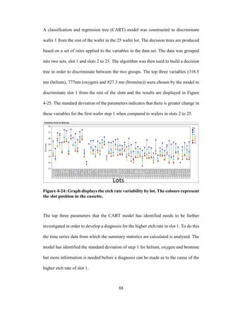
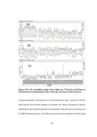
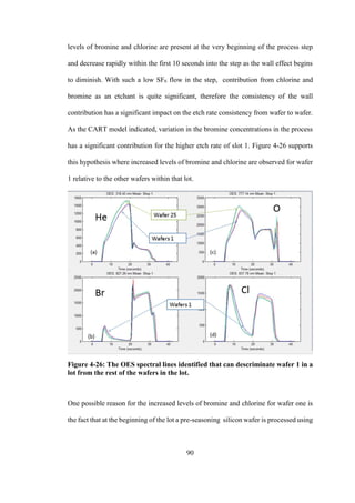
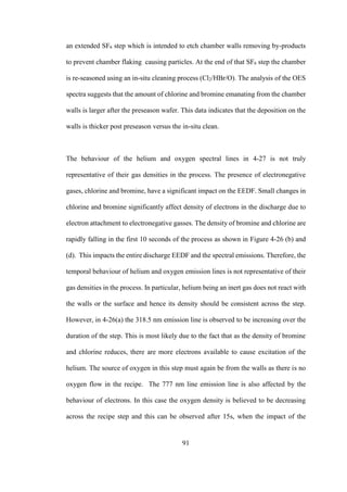
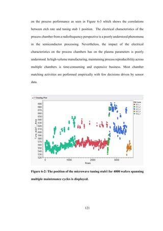
This thesis presents new techniques to diagnose process variability in industrial plasma etching systems. Optical emission spectroscopy and electrical sensors are used to measure plasma parameters during etching. Statistical analysis methods like principal component analysis and gradient boosting trees are applied to sensor data to correlate variability in etch rate with measurements. A case study of an etching process is presented where time series OES data is analyzed across process steps. Variability due to the "first wafer effect" is investigated. Process excursions are also examined by studying shifts in principal components. The combination of in-situ sensors and statistical analysis provides a powerful tool for process engineers to diagnose sources of variability.


![x
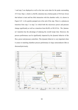
Figure 2-3:Plasma potentials Vp(t) ( solid curves) and excitation electrode voltage
V(t) (dashed curves), assuming purely capacitive RF sheath behavior, for three
system geometries and for DC coupled and capacitively coupled excitation
electrodes.[6].............................................................................................................. 10
Figure 2-4: Schematic representation of the voltages in an AC coupled asymmetric
RF plasma. a). Maximum RF voltage condition, b) minimum RF voltage condition.
Vp is the plasma potential [6]. ................................................................................... 13
Figure 2-5:The schematic shows the relationship between the phase in the RF cycle
that the ion enters the sheath and the resultant energy gained the ion as it accelerates
crossing the sheath[6]................................................................................................. 15
Figure 2-7: Total inelastic (σinel) and ionization (σi )cross sections for electrons in
nitrogen [15]............................................................................................................... 18
Figure 2-8: Simplified schematic of isotropic etching of silicon surface in SF6/He
discharge. ................................................................................................................... 21
Figure 2-9: The four fundamental etching mechanisms. І. Physical sputtering, ІІ.
Chemical, ІІІ. Ion Enhanced, ІV. Ion enhanced inhibitor [21]. ................................. 23
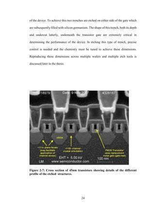
Figure 2-10: Cross section of 45nm transistors showing details of the different
profile of the etched structures.................................................................................. 24
Figure 2-11: SEMS cross section of metal etch stack with photoresist and Si3N4 hard
marks at 20 and 90 seconds into the etch process. SEMs show the erosion of the
photoresist mask showing the need for the hardmask ............................................... 26
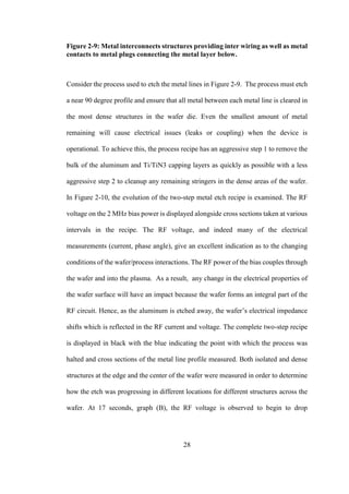
Figure 2-12: Metal interconnects structures providing inter wiring as well as metal
contacts to metal plugs connecting the metal layer below......................................... 28](https://image.slidesharecdn.com/750f8846-02d9-4e6c-84da-231f8478ab05-161124161834/85/NMacgearailt-Sumit_thesis-10-320.jpg)
![xi
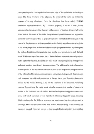
Figure 2-13: The evolution of the metal etch process. The endpoint signal on the left
RF Voltage of the 2MHz RF bias displayed on the right the corresponding cross
sections of the center and edge of the wafer dense and isolated structures. .............. 30
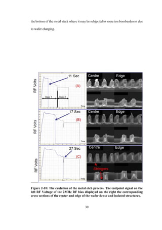
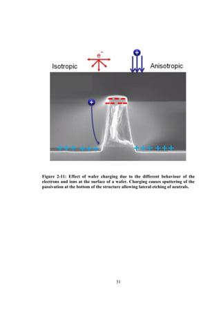
Figure 2-14: Effect of wafer charging due to the different behaviour of the electrons
and ions at the surface of a wafer. Charging causes sputtering of the passivation at
the bottom of the structure allowing lateral etching of neutrals. ............................... 31
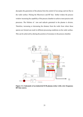
Figure 3-1: Schematic of an industrial ECR plasma etcher with a low frequency RF
bias source.................................................................................................................. 33
Figure 3-2; Magnetron Resonator. (http://www.cpii.com/) ....................................... 35
Figure 3-3: Cross sections of a magnetron showing the cavities and the cathode. The
two permanent magnets are positioned on the top and bottom of the cavities. Also
displayed is the alternating voltage to heat the filament the negative DC voltage
applied to the cathode[38].......................................................................................... 36
Figure 3-4: Plasma modeling completed by Kushner et al[42]. The simulations show
the power deposition, electron temperature and density in ECR reactor................... 39
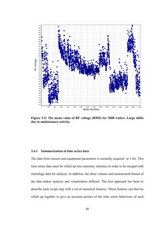
Figure 3-5: The mean value of RF voltage (RMS) for 3000 wafers. Large shifts due
to maintenance activity. ............................................................................................. 46
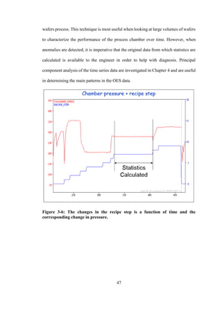
Figure 3-6: The changes in the recipe step is a function of time and the corresponding
change in pressure...................................................................................................... 47
Figure 3-7: This two-dimensional representation of principal component 1 and 2
capturing most of the variability in the data set[48]. ................................................. 48
Figure 3-8: The score for each observation is the distance to the PC (a). The loading
for each PC is the angle each variables is from the PC[49]....................................... 49](https://image.slidesharecdn.com/750f8846-02d9-4e6c-84da-231f8478ab05-161124161834/85/NMacgearailt-Sumit_thesis-11-320.jpg)
![xii
Figure 3-9: Shows a simple decision tree to predict the weather (Y) from
temperature( X1), humidity (X2) and dew- point(X3)[51]........................................ 51
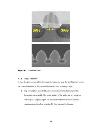
Figure 4-1. Transistor Gate ........................................................................................ 54
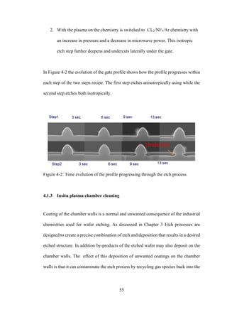
Figure 4-2: Time evolution of the profile progressing through the etch process....... 55
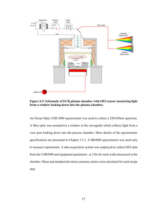
Figure 4-3: Schematic of ECR plasma chamber with OES sensor measuring light
from a window looking down into the plasma chamber............................................ 57
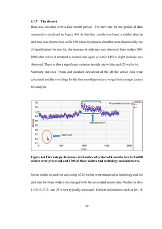
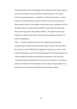
Figure 4-4 Etch rate performance of chamber of period of 4 months in which 6000
wafers were processed and 1700 of these wafers had metrology measurements. ..... 59
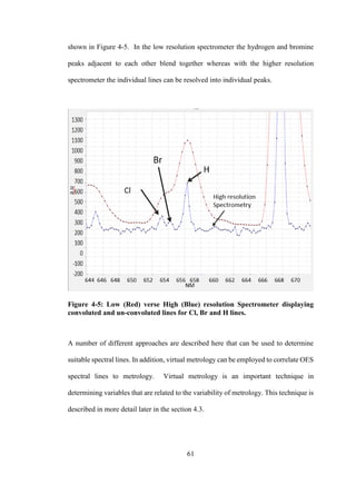
Figure 4-5: Low (Red) verse High (Blue) resolution Spectrometer displaying
convoluted and un-convoluted lines for Cl, Br and H lines....................................... 61
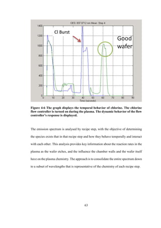
Figure 4-6 The graph displays the temporal behavior of chlorine. The chlorine flow
controller is turned on during the plasma. The dynamic behavior of the flow
controller’s response is displayed. ............................................................................. 63
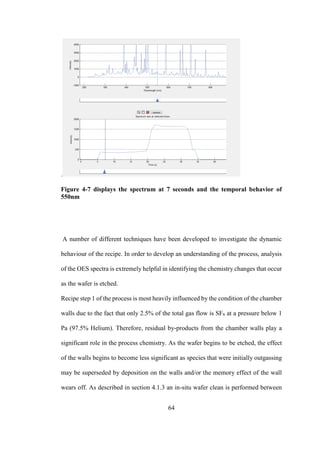
Figure 4-7 displays the spectrum at 7 seconds and the temporal behavior of 550nm64
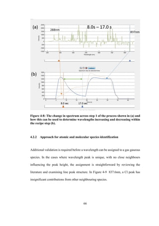
Figure 4-8: The change in spectrum across step 1 of the process shown in (a) and
how this can be used to determine wavelengths increasing and decreasing within the
recipe step (b)............................................................................................................. 66
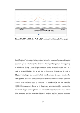
Figure 4-9: 837nm Chlorine Peak red (7 sec, blue17sec) in step1 of the recipe........ 67
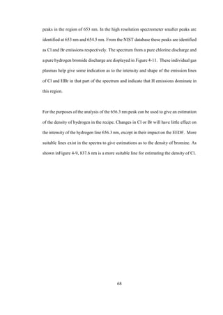
Figure 4-10: shows the peak structure for 656 nm and 654 nm (a) and also the time
series traces for the same wavelengths in (b)............................................................. 69
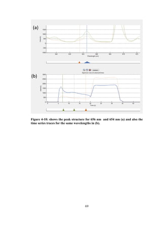
Figure 4-11. Individual spectrum shapes structures of Cl2 and HBr discharges run
independently............................................................................................................. 70
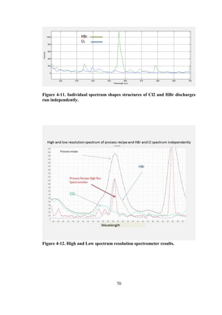
Figure 4-12. High and Low spectrum resolution spectrometer results. ..................... 70](https://image.slidesharecdn.com/750f8846-02d9-4e6c-84da-231f8478ab05-161124161834/85/NMacgearailt-Sumit_thesis-12-320.jpg)


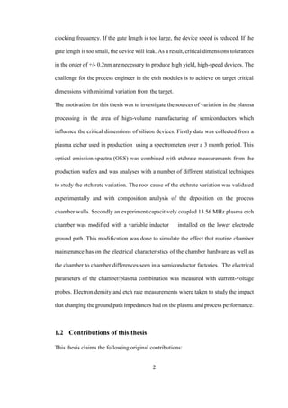


![6
2 Chapter 2
Industrial RF Plasma processing
2.1 Introduction
RF plasmas have been widely adopted in semiconductor manufacturing due to their
ability to create and control complex chemistry which is used to manipulate and
modify surface properties of silicon wafers. This chapter examines the basic principles
of plasmas and gives a background to the etching mechanisms used in industrial
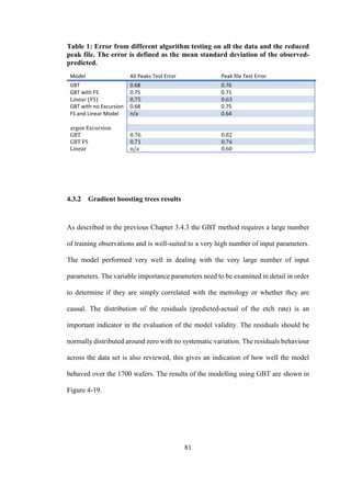
plasma processing tools.
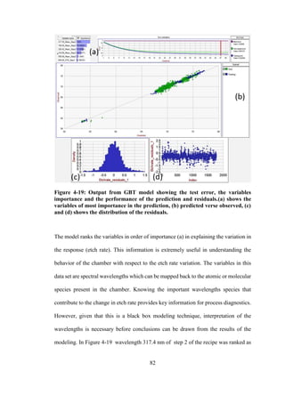
The term plasma, coined by Irving Langmuir [1], is used to describe quasi-neutral gas
containing equal numbers of positive and negatively charged particles. As a substance
is heated to a sufficiently high temperature, the molecules in the gas decompose into
atoms. As the temperature is further increased, the atoms ionize into freely moving
charged particles as the gas transitions into a plasma state. The temperature required
to form plasma is many thousands of kelvin. Direct heating on the gas is not a viable
option and heating is typically done by electrical means.
Industrial plasma processing equipment primarily deal with weakly ionized plasma
discharges which are driven by a radio frequency (RF) voltage supply that drives
current through a low-pressure gas. This applied power preferentially heats the mobile](https://image.slidesharecdn.com/750f8846-02d9-4e6c-84da-231f8478ab05-161124161834/85/NMacgearailt-Sumit_thesis-23-320.jpg)
![10
Figure 2-1:Plasma potentials Vp(t) ( solid curves) and excitation electrode
voltage V(t) (dashed curves), assuming purely capacitive RF sheath behavior, for
three system geometries and for DC coupled and capacitively coupled excitation
electrodes.[6]](https://image.slidesharecdn.com/750f8846-02d9-4e6c-84da-231f8478ab05-161124161834/85/NMacgearailt-Sumit_thesis-27-320.jpg)
![12
2.2.2 The capacitive RF sheath
The driving frequency of 13.56 MHz has a period of 74 ns. The ion and electron plasma
frequencies are given by [2]:
𝜔 𝑝𝑖 = (
𝑒2
𝑛𝑖
∈0 𝑚𝑖
)
1
2
2.1
𝜔 𝑝𝑒 = (
𝑒2
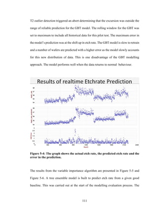
𝑛 𝑒
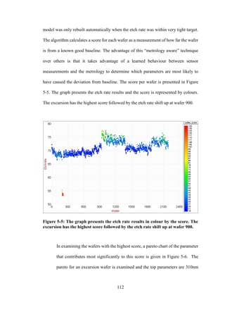
∈0 𝑚 𝑒
)
1
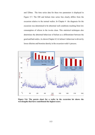
2
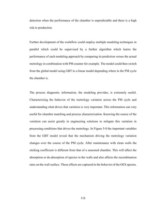
2.2
where ni and ne are the ion and electron densities and mi and me are the masses of the
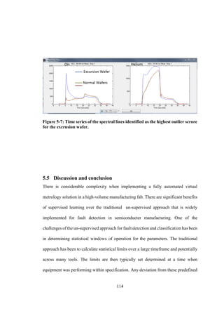
ions and electrons respectively. For normal plasma conditions where ni=ne the ion and
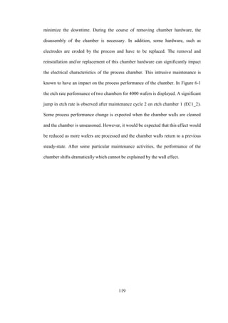
plasma frequency are in the order of 3 MHz and 300 MHz respectively (for a plasma
density of 1015
m-3
measured with a hairpin probe in Chapter 6). The electrons respond
almost instantaneously to the oscillating electric field in the sheath, whereas the ions
respond to the time average fields.
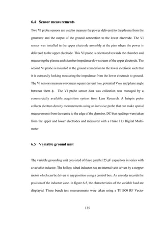
In Figure 2-2 the voltages potential experienced by the powered and grounded
electrodes as a function of sinusoidal RF voltage is displayed. The sheath width
expands and contracts on both electrodes within the RF cycle. The plasma potential
also oscillates.](https://image.slidesharecdn.com/750f8846-02d9-4e6c-84da-231f8478ab05-161124161834/85/NMacgearailt-Sumit_thesis-29-320.jpg)
![13
Figure 2-2: Schematic representation of the voltages in an AC coupled
asymmetric RF plasma. a). Maximum RF voltage condition, b) minimum RF
voltage condition. Vp is the plasma potential [3].
The electron density in the RF sheath changes with the instantaneous voltage.
Electrons move in and out of the sheath region when the sheath momentarily collapses
as the electrode potential approaches the plasma potential (Vp) allowing electrons to
escape and balance the ion current.
2.2.3 Ion Energy Distribution
The energy with which ions impinge on the wafer surface is a critical parameter in any
plasma process. In particular, ion bombardment plays a critical role in reactive ion
etching. The ion transit time to cross the sheath is given by [4]:](https://image.slidesharecdn.com/750f8846-02d9-4e6c-84da-231f8478ab05-161124161834/85/NMacgearailt-Sumit_thesis-30-320.jpg)
![15
Figure 2-3:The schematic shows the relationship between the phase in the RF
cycle that the ion enters the sheath and the resultant energy gained the ion as it
accelerates crossing the sheath[3].
2.2.4 Electron heating
There are two main mechanisms for heating electrons in RF capacitively coupled
discharges: ohmic (collisional) and stochastic heating. Plasma resistivity due to](https://image.slidesharecdn.com/750f8846-02d9-4e6c-84da-231f8478ab05-161124161834/85/NMacgearailt-Sumit_thesis-32-320.jpg)
![16
electron-neutral collisions leads to ohmic heating while momentum transfer from high
voltage moving sheaths leads to stochastic heating. Thus, ohmic heating is mainly a
bulk phenomenon while stochastic heating is localized in the sheath regions.[5]
In the higher pressure regimes (100-500mTorr) of capacitively coupled RF discharges
studied in this thesis, ohmic heating is the predominant mechanism for the transfer of
energy to the electrons. This energy transfer, from the electric field to the electrons,
occurs in the bulk due to the elastic electron-neutral collisions. The energy is gained
by an electron in the oscillating electric field and is transferred into a direction
perpendicular to the field and it is not lost during the reversal of the electric field[6][7].
In this pressure regime, secondary electron emission may still occur with the majority
of electrons traversing the sheath without collisional ionization and penetrating the
bulk plasma with energies above the ionization threshold. The surf riding mechanism
of the oscillating sheath edge can also heat electrons. During the second half of the RF
cycle the sheath spatially extends back into the bulk, accelerating electrons into the
plasma [8][9].
2.2.5 Electron – Ion collisions:
In this section some of the basic processes involving electrons and ions are reviewed
to give an understanding of the basic mechanisms. It is by no means an exhaustive
review of the complex interactions that occur in the discharge, but is mainly focused
on those processes which are most important to plasma processing.
Collisional processes can be divided into elastic and inelastic collisions. An elastic
collision is one in which kinetic energy is conserved. In the collinsion between an
electron and an atom the different in mass is such that the energy transfer is negliable](https://image.slidesharecdn.com/750f8846-02d9-4e6c-84da-231f8478ab05-161124161834/85/NMacgearailt-Sumit_thesis-33-320.jpg)
![17
and the electron just changes direction. If the electron is moving in an electric field the
collision just servers to restric the velocity in direction of the field. If the electron
energy is above the ionization threshold, the impinging electron may remove an
electron from the atom resulting in an ion and two electrons.
The three primary electron loss mechanisms are recombination, attachment and
diffusion. In electron attachment, there is a significant loss mechanism in the
electronegative gas regimes (O, Cl, F ,Br) used in plasma processing where electrons
are lost in the creation of negative ions. The electronegative gases have a quenching
effect and a significant impact on the resultant plasma properties, specifically the
EEDF and plasma emissions observed in Optical emission spectroscopy.
2.2.6 Collisional Cross Sections.
The collisional process between electrons and particles needs to consider how the
particle presents itself to an approaching electron. The atom consists of a nucleus in
the centre and an assembly of electrons orbiting around a large empty space. The
interaction between the approaching electron and the particle is strongly dependent on
the electrostatic forces and thus depends strongly on the velocity of the approaching
electron. There is a certain element of probability and uncertainty about the interaction
that can occur in the collision. This probability is represented as the collisional cross-
section of the particle. The collisional cross-section is a more useful parameter then
the mean free path [10]. Figure 2-4 gives the cross section for nitrogen as a function](https://image.slidesharecdn.com/750f8846-02d9-4e6c-84da-231f8478ab05-161124161834/85/NMacgearailt-Sumit_thesis-34-320.jpg)
![18
of the electron energy. The cross section of neutral Nitrogen atoms is much different
from that of the Nitrogen ion. The dependence of the electron energy has a dramatic
effect on the collisional probability.
Figure 2-4: Total inelastic (σinel) and ionization (σi )cross sections for electrons
in nitrogen [11].
2.2.7 The electron energy distribution function (EEDF)
The Maxwell Boltzmann distribution applies to an assembly of particles that are in
complete thermal equilibrium. Electrons in a plasma discharge are not in a state of
equilibrium. Slow electrons make elastic collisions while electrons with energies
above excitation and ionization thresholds are involved in inelastic collisions [10].
Electrons also diffuse to the wall and have different heating mechanisms which result
in the wide distribution of energies. Many studies have been completed to determine](https://image.slidesharecdn.com/750f8846-02d9-4e6c-84da-231f8478ab05-161124161834/85/NMacgearailt-Sumit_thesis-35-320.jpg)
![19
the EEDF for a variety of processing conditions[12]. The addition of electronegative
gas species to the discharge can also affect the EEDF. Many studies have measured a
hot tail in the distribution which is responsible for much of the ionization[13][14].
2.3 Plasma etching
Plasma etching’s popularity in the manufacturing of semiconductor devices has grown
greatly since the 1960s. As an alternative to wet chemical processing, plasma etching
has a number of advantages. In addition to the environmental benefits of moving away
from chemical baths, in which batches of wafers would be processed together, plasma
etching offers a cleaner more efficient and controllable environment for removing
material from the surface of silicon wafers. With the reduction in dimensions of
semiconductor devices, plasma etching offers the only commercially viable solution.
High-volume manufacturing of 14nm devices would be impossible without plasma
processing. Plasma etching provides anisotropic etching with a very high degree of
control and the ability to selectively etch one material in preference to another.
2.3.1 Processing requirements
The challenge for process engineers is to develop a process capable of etching
submicron features, meeting all the dimensional tolerances of the feature size, while
maintaining a high degree of repeatability. The challenges for plasma etching are:
1. The etch rate of the process must be as fast as possible in order to maximize
the throughput of the plasma etch tool.
2. Critical dimensions of the feature must be achieved.](https://image.slidesharecdn.com/750f8846-02d9-4e6c-84da-231f8478ab05-161124161834/85/NMacgearailt-Sumit_thesis-36-320.jpg)
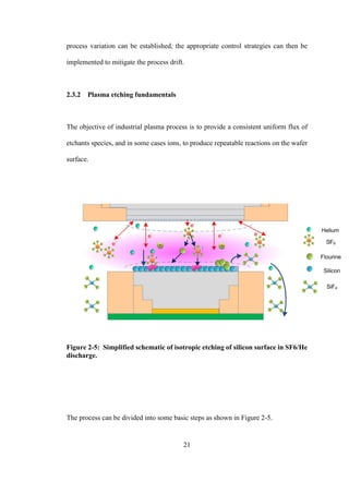
![22
1. Firstly, radicals and ions are produced from feedstock gasses. This process is
governed by the electron collisional processes. The electron density and
temperature and ultimately the electron collisional rate[15] are the
important parameters that determine the density of ions and radicals.
2. The transportation of the reactive radicals from the plasma bulk to the surface
of the wafer is through a diffusion process. The size of the chamber, gas flow
rates and pressure setpoint also determines whether the radical will have a
collision before making it to the wafer surface. The chamber is designed with
a shower head and baffle plate configurations to facilitate the delivery of the
feed gases in such a way as to compensate for the greater
loading/consumption of radicals in the centre of the wafer compared with the
edge[16].
3. The flux of ions directed towards the wafer surface will enhance the reaction
of the neutral radicals with the wafer surface. The ions provide energy that
break the bonds of the substrate material creating an active etching site. In
addition, any polymerization or passivation film that develops on the wafer
surface will also be sputtered off the horizontal surfaces by the ion flux.
4. The reactive species (fluorine radicals for example) are absorbed onto the
surface and react chemically. In the case of fluorine etching silicon, atomic
fluorine penetrates approximately five monolayers into the bulk, resulting in a
volatile by-product (SiF4) or its precursors (SiF,SiF2, SiF3)[17][9][18].
5. The volatile by-products need to be de-absorbed from the surface of the wafer
and are pumped out the chamber. This process is assisted by ensuring low
residence time in high flow process conditions.](https://image.slidesharecdn.com/750f8846-02d9-4e6c-84da-231f8478ab05-161124161834/85/NMacgearailt-Sumit_thesis-39-320.jpg)
![23
The mechanism of etching three dimensional features involves some additional
complexity. In Figure 2-6 the basic etch mechanisms are shown. In order to achieve a
vertical profile, sidewall passivation is required to prevent neutral radicals from
etching the feature horizontally. The process chemistry and plasma parameters are
deliberately tuned so as to produce the right amount of passivation of the side wall to
balance the vertical etching. Too much passivation and the profile will taper. Too little
and it will bow.
Figure 2-6: The four fundamental etching mechanisms. І. Physical sputtering, ІІ.
Chemical, ІІІ. Ion Enhanced, ІV. Ion enhanced inhibitor [17].
This carefully engineered balance of vertical etching and lateral passivation determines
the profile of the etched structure. Figure 2-7 shows the cross section of the transistors
and first metal interconnects of a 45nm semiconductor device. While 90° profiles are
desired in the etching of the gate features, other structures demand tapered profiles.
For example, silicon germanium is used on either side of the channel under the gate to
stress the silicon lattice to improve electron mobility and increase the clocking speed](https://image.slidesharecdn.com/750f8846-02d9-4e6c-84da-231f8478ab05-161124161834/85/NMacgearailt-Sumit_thesis-40-320.jpg)
![25
2.3.3 Other considerations for plasma etching
2.3.3.1 Lithography and Photoresist
Lithography and Photoresist are a vital component in the patterning of semiconductor
devices. The ability of plasma etching to produce smaller feature size is dependent on
the ability of the lithographer to provide imaging solutions that can create smaller and
smaller patterns in photoresist which act as a mask for plasma etching. To deal with
the reduction in line width, lithography has increased the numerical aperture of the
lens and reduced the wavelength of the illumination used to expose the
photoresist[19]. To accommodate shorter wavelengths of the illuminated source the
photoresist thickness and robustness has been reduced. As a result of these changes to
the mask materials and thickness, as well as the large cost associated with printing for
small featured masks, significant changes have been made in plasma etching. Firstly,
to deal with the reduced robustness of the photoresist, a hard mask is introduced into
the process flow. This thin sacrificial layer of silicon nitride, for example, upon which
the plasma process transfers the mask from the photoresist to the hard mask using a
chemistry which etches away the hard mask except where it is covered by the
photoresist. The mask integrity is now maintained by the more robust hard mask
enabling harsh processing conditions for a long duration during which the photoresist
would have been eroded away. The other option is to trim the photoresist before
transferring the pattern. Using a isotropic oxygen discharge, the dimensions of the
photoresist mask can be reduced [20]. The technique means that lithography can print
a line of 65nm which can be “trimmed” to 50nm resulting in a 50nm etched feature.](https://image.slidesharecdn.com/750f8846-02d9-4e6c-84da-231f8478ab05-161124161834/85/NMacgearailt-Sumit_thesis-42-320.jpg)
![26
This technique is especially useful in extending the lifetime of older lithography
equipment.
Figure 2-8: SEMS cross section of metal etch stack with photoresist and Si3N4
hard marks at 20 and 90 seconds into the etch process. SEMs show the erosion of
the photoresist mask showing the need for the hardmask .
2.3.3.2 Selectivity and within wafer uniformity:
Selectivity of a process is the ability to etch one material preferentially over other
materials. In plasma etching, selectivity to underlying thin etch stop layers is critical
in preventing damage to underlying structures and have been studied extensively[21]–
[25]. In Figure 2-8 high selectivity of Aluminium over Si3N4 is required to prevent
the hard mask from being etched during the process and having an impact on the profile
of the metal line. Selectivity to the underlying silicon is critical to minimise damage
to the surface. Tuning a process to achieve the required selectivity is mostly achieved
by tuning the chemistry. If selectivity to an underlying layer is required, the process
can be endpointed[26] upon the first signs of breakthrough to the underlying layer.
Endpointing can be achieved by monitoring the optical emissions of a particular](https://image.slidesharecdn.com/750f8846-02d9-4e6c-84da-231f8478ab05-161124161834/85/NMacgearailt-Sumit_thesis-43-320.jpg)
![27
plasma species or an electrical signal of the RF power [27]. The process chemistry can
immediately be modified upon the detection of the breakthrough to be more selective
to the underline layer. In the etching of polysilicon gates using Cl2/HBr, oxygen is
added to improve selectivity to the underlying SiO2 gate oxide stop layer[18]. The bias
power is also lowered to reduce the ion bombardment and allow the oxygen to defuse
into the thin gate oxide promoting oxide growth. Pulsing the RF wafer bias has also
been successful in improving the selectivity. The ability to control the ion energy and
flux to the wafer surface can significantly improve selectivity[28] . Pulsed plasmas
have also been successful in alleviating the issue of notching at the interface of
conductive films (polysilicon and aluminium). Notching can also occur at the interface
between underlying dielectric films (SiO2) and the polysilicon gate. Wafer charging,
caused by the charging of the polysilicon line, influences the ion trajectory arriving at
the surface of the wafer [29]. Pulsing the RF bias allows the charge build-up to
dissipate when the RF bias is momentarily turned off.](https://image.slidesharecdn.com/750f8846-02d9-4e6c-84da-231f8478ab05-161124161834/85/NMacgearailt-Sumit_thesis-44-320.jpg)
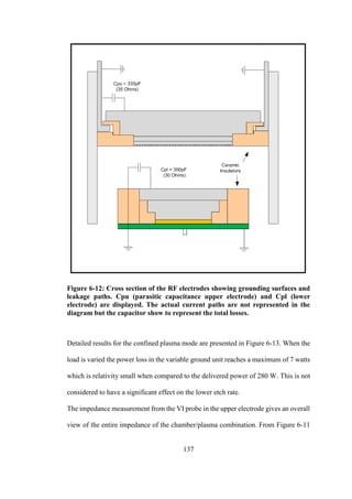
![32
3 Chapter 3
Process Equipment, Sensors and Statistics
3.1 Introduction
In this chapter the basic principles of the electron cyclone resonance (ECR) plasma
reactors are discussed, in particular, the hardware used for industrial plasma
processing. The sensors used for the diagnostic measurements are explained and the
statistical approaches used to process the sensor data and correlation techniques are
discussed.
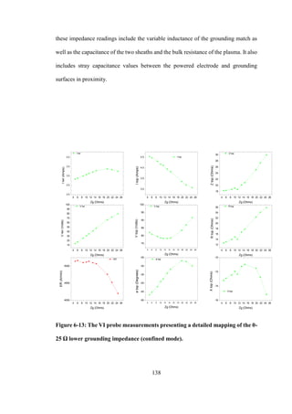
3.2 Electron Cyclotron Resonance plasma sources
Electron Cyclotron Resonance (ECR) plasmas have been in use since the early 1960s
for space craft propulsion applications [30]. Suzuki et al. first published the application
of a microwave source for plasma etching in 1977 [31]. They have been commercially
available in semiconductor factories from the mid-1980s. The main attraction of an
ECR plasma source is the ability to generate a high degree of ionization (>10%) at low
pressure. Since ECR plasma sources do not rely on a current flowing from an electrode,
this offered the opportunity to generate the plasma remotely from the wafer surface.
Thus, this minimized the damage to the wafer surface from ion bombardment or device
damage from wafer charging issues. The ECR source also allows for the opportunity
to independently bias the wafer using a low frequency RF power supply. This](https://image.slidesharecdn.com/750f8846-02d9-4e6c-84da-231f8478ab05-161124161834/85/NMacgearailt-Sumit_thesis-49-320.jpg)
![34
3.2.1 The magnetron
Magnetron technology was invented by Albert Hull in 1920 in the US. At the start of
WWII, John Randall and Harry Boot at Birmingham University were contracted to
develop a short wavelength power source for radar application. They invented an 8
concentric cavity magnetron[32]. The magnetron is a high-powered oscillator which
converts potential energy of the electron cloud in the cathode into high-frequency radio
waves. The magnetron consists of a cathode in the center surrounded by cavities which
act as an anode. A perpendicular magnetic field is provided by permanent magnets
which are placed on the top and bottom of the magnetron as depicted in Figure 3-3.
The source of electrons is a heated cathode made from a thermionic material. A high
current (~20 A, ~5 V) AC power supply heats the filament which emits electrons. A
DC offset of -5KV is applied to the cathode. The E field between the cathode and
anode acts on the free electrons accelerating them towards the anode. The permanent
magnets mounted at the top and bottom of the magnetron exert a perpendicular B force
on the electrons which when combined with the E field horizontal force causes the
electrons to spiral away from the cathode in paths of varying curvature. Cavities that
are placed around the cathode are designed to specific physical dimensions.
Electrically, the cavity appears as an inductor and a capacitor in parallel and forms a
resonance circuit. The physical makeup of the cavity determines the resonating
frequency output of the magnetron. As this cloud of electrons approaches the anode, it
falls under the influence of the RF fields at the vane tips and electrons will either be
retarded in velocity, if they happen to face an opposing RF field, or accelerated if they
are in the vicinity of an aiding RF field. Since the force on an electron due to the
magnetic field B is proportional to the electron velocity through the field, the retarded](https://image.slidesharecdn.com/750f8846-02d9-4e6c-84da-231f8478ab05-161124161834/85/NMacgearailt-Sumit_thesis-51-320.jpg)
![35
velocity electrons will experience less "curling
force" and will therefore drift toward the anode,
while the accelerated velocity electrons will curl
back away from the anode[33]. Every other
cavity is connected together and in turn
connected to an antenna which protrudes from
the magnetron.
Figure 3-2; Magnetron
Resonator.
(http://www.cpii.com/)](https://image.slidesharecdn.com/750f8846-02d9-4e6c-84da-231f8478ab05-161124161834/85/NMacgearailt-Sumit_thesis-52-320.jpg)
![36
Figure 3-3: Cross sections of a magnetron showing the cavities and the cathode.
The two permanent magnets are positioned on the top and bottom of the cavities.
Also displayed is the alternating voltage to heat the filament the negative DC
voltage applied to the cathode[34].
3.2.2 Microwave tuner controller
The function of the microwave tuner is to provide accurate measurement of the
forward and reflected power from the plasma. Aditionally, a three stub tuner provides
varying capacitance to resonate with the varying inductance of the ECR chamber. A
voltage standing wave detector is mounted in the waveguide which consists of diodes](https://image.slidesharecdn.com/750f8846-02d9-4e6c-84da-231f8478ab05-161124161834/85/NMacgearailt-Sumit_thesis-53-320.jpg)
![37
placed at 1/6 λ which feeds the signals into the microwave controller. The
measurement of the standing wave voltage allows the calculation of the progressive
power propagating towards the plasma and the reflected wave returned from the
chamber/plasma combination. The tuner also calculates insertion lengths of the three
stubs which are inserted into the waveguide to minimize the reflections. The measured
forward power is compared to the recipe setpoint and adjusts the high-voltage DC
current to the magnetron to deliver the required power to the plasma. As part of the
calculations, the tuner also calculates the reflection coefficients which are a very
useful diagnostic measurement as it gives an electrical impedance that the
plasma/chamber combination presents to the microwave power[35].
3.2.3 Electron cyclon resonance.
The 2.45 GHz high-frequency electromagnetic wave generated by the magnetron and
transmitted through the waveguide is introduced into the reaction chamber through a
quartz window. A magnetic field is generated in the reaction chamber through three
sets of electromagnetic coils, two placed around the chamber and one on the top.
Electrons rotate around the magnetic lines of force with an electron cyclotron angular
frequency given by the equation:
𝜔𝑐 =
𝑒𝐵
𝑚 𝑒
3.1
where 𝑒 is the electric charge, 𝑚 𝑒 is the mass of an electron and 𝐵 is the magnetic
field[9]. The electric field of the 2.45 GHz microwave delivered through the
waveguide is superimposed on the perpendicular magnetic field lines generated by the
electromagnets. At 87.5mT magnetic flux density, the 2.45 GHz microwave:e will](https://image.slidesharecdn.com/750f8846-02d9-4e6c-84da-231f8478ab05-161124161834/85/NMacgearailt-Sumit_thesis-54-320.jpg)
![38
cause the electrons to rotate at 2.45 GHz around the magnetic field lines. As the
electrons are spiralling around the magnetic field lines, they continuously accelerate
achieving very high energies. This resonance zone is where the microwave energy is
strongly absorbed. Magnetic flux density higher than the 875 Gauss is required in the
source region of the vacuum window above in order to facilitate the propagation of the
microwaves into the vacuum chamber before reaching the dampening of the ECR
zone[36]. In Figure 3-4 Kushner’s [37] simulation of an ECR chamber is displayed.
The results show that most of the microwave power is absorbed in the resonance zone
accelerating electrons to very high energies. These electrons then collide with the
neutral gases causing a high degree of ionization. The influence that the magnetic field
lines have on the charged particles is clearly seen in the ionization rate and electron
density results of the simulation.](https://image.slidesharecdn.com/750f8846-02d9-4e6c-84da-231f8478ab05-161124161834/85/NMacgearailt-Sumit_thesis-55-320.jpg)
![39
Figure 3-4: Plasma modeling completed by Kushner et al[38]. The simulations
show the power deposition, electron temperature and density in ECR reactor.
The electrode upon which the wafer is electrostatically clamped is connected to a 400
kHz RF power supply. As discussed in Chapter 2, 400 kHz frequency is below the ion
frequency and therefore the ions will be influenced by the modulation of the sheath
voltage. The 2.5μs period of the RF cycle is slow enough to allow ions to transition](https://image.slidesharecdn.com/750f8846-02d9-4e6c-84da-231f8478ab05-161124161834/85/NMacgearailt-Sumit_thesis-56-320.jpg)
![40
across the sheath bombarding the surface of the wafer. The RF is controlled to a power
setpoint. An electrostatic chuck used to clamp the wafer to the electrode facilitates
high-pressure helium to be delivered to the gap between the electrode and the wafer,
thus, enabling heat transfer from the wafer to the water cooled electrode.
3.3 Measurement techniques
The adoption of sensors in industrial plasma reactors has not progressed relative to the
capability developed in academia for plasma diagnostics. Process equipment
manufacturers have always measured equipment parameters such as pressure, power,
temperature, etc. in order to control the equipment. It also provides some basic
alarming if process setpoints have not been achieved. In the 1990s a generic protocol
for communication and control of semiconductor manufacturing equipment was
agreed upon and the development of software began that could record the equipment
parameters[39]. However, few of these parameters relate to the process and
measurement of the process parameters in the industry remains relatively poor. The
availability of robust process sensors and the necessary software modeling to interpret
the data has limited implementation of advanced sensors in the industry. Many plasma
diagnostic sensors are intrusive and cannot be used in a manufacturing environment.
In addition, the corrosive chemistries used for industrial processes also limits the
choice of sensors. In this section two non-invasive measurement techniques will be
discussed along with two invasive sensors that are used for some fundamental
characterization.](https://image.slidesharecdn.com/750f8846-02d9-4e6c-84da-231f8478ab05-161124161834/85/NMacgearailt-Sumit_thesis-57-320.jpg)
![42
3.3.2 Current voltage probes
The electrical characteristics of the plasma process and hardware combination is
another useful diagnostic measurement. The electrical measurement is usually taken
between the RF matching unit and the powered electrode. A sample of the voltage
waveform is capacitively coupled to a detector and a sample of the RF current wave
form is usually inductively coupled to the detector. Both signals are processed and the
phase angle between the current and voltage is also calculated. Harmonics of the
fundamental frequency are generated by the nonlinearity of the modulation of the
plasma sheath and can be measured and calculated using Fourier analysis. Harmonics
measured by the VI probe are very sensitive to small changes in the sheath. If the wafer
is placed on the powered electrode, RF harmonics have shown to be able to detect
0.5% open area endpoint[40]. Other studies of the harmonics have shown them useful
in modelling the sheath behaviour [41]. Useful data from the VI probe is used to
measure the actual power delivered to the electrode which can determine the losses in
the match and delivery system as well as the determining the real and imaginary
elements of the plasma/hardware combination which is detailed later in Chapter 6.
3.3.3 Hairpin probe
A microwave hairpin resonator (hairpin probe) has been established as an effective
way of measuring electron density in plasmas. The hairpin probe is an open-ended u-
shaped quarter wavelength transmission line. When a suitable frequency signal source](https://image.slidesharecdn.com/750f8846-02d9-4e6c-84da-231f8478ab05-161124161834/85/NMacgearailt-Sumit_thesis-59-320.jpg)
![43
is applied to the short end of the probe, maximum power coupling takes place. This
specific frequency is a quarter wavelength which equals the length of the pins. The
resonance frequency is related to the dielectric constant of the medium that surrounds
the probe.
The resonance frequency of the hairpin probe is given by [42]
𝑓𝑟 =
𝑐
4𝐿√𝜖
=
𝑓0
√∈
3.2
where c is the speed of light, and L is the length of the resonator and ∈ is the
permittivity of the surrounding medium. Plasma can also be treated as a dielectric. If
the thermal motion of electrons can be considered weak as compared to the electric
field set-up between the pins, then one can model the plasma permittivity based on
cold plasma approximation, which ignores the thermal motion of electrons. At low
pressures, the electron neutral mean free path can be larger than the separation between
the pins. Hence plasma permittivity can be given by [2]:
∈ 𝑝= 1 −
𝑓𝑝
2
𝑓2
3.3
where 𝑓𝑝 is the plasma frequency. By substituting equation 3.2 into equation 3.3 the
resonance frequency of the plasma can be expressed by:
𝑓𝑟
2
= 𝑓0
2
+ 𝑓𝑝
2 3.4](https://image.slidesharecdn.com/750f8846-02d9-4e6c-84da-231f8478ab05-161124161834/85/NMacgearailt-Sumit_thesis-60-320.jpg)
![44
The above equation can be further simplified [2][42]:
𝑛 𝑒 =
𝑓𝑟
2
− 𝑓0
2
𝑒2 𝜋𝑚 𝑒⁄
3.5
where 𝑛 𝑒 is the electron density, 𝑒 is the electronic charge, 𝑚 𝑒 is the mass of and
electron and 𝑓𝑟 is the resonance frequency of the plasma and 𝑓0 is the resonance
frequency of the probe at vacuum.
Data collection with a hairpin probe involves inserting an invasive probe into the
plasma discharge. While this is not feasible in a production environment, it is possible
to take the equipment off-line to make measurements. A microwave generator provides
a sweeping signal from 2 to 3.8 GHz. The reflections are measured on an oscilloscope.
The resonance point is measured at vacuum and then again under plasma conditions.
The change in frequency from vacuum to plasma is used in equation 3.5 to determine
the electron density.
3.4 Statistical analysis techniques
Statistics have a long history of implementation in semiconductor manufacturing.
Statistical process control (SPC) has been widely used to set critical manufacturing
parameters. More recently, with the availability of equipment parameters from](https://image.slidesharecdn.com/750f8846-02d9-4e6c-84da-231f8478ab05-161124161834/85/NMacgearailt-Sumit_thesis-61-320.jpg)
![48
3.4.2 Principal Components Analysis
Principal component analysis (PCA) is an unsupervised dimensionality reduction
technique that extracts explanatory variables from the data and is especially useful for
exploring the variation in the data sets and finding patterns.
In figure 3-7, a two dimensional dataset (x,y) is shown in (a). The principal component
analysis can be considered as a rotation of the axis of the original coordinate system
to new orthogonal axis that coincides with direction of maximum variation[43].The
construction of the two principle components (PC’s) which pass through the direction
of maximum variation are shown in Figure 3-7. Projecting each observation onto the
principle component (PC), the distance to the PC gives a score for each observation.
Figure 3-7: This two-dimensional representation of principal component 1 and 2
capturing most of the variability in the data set[44].
The angle between the PC’s and the original variables is calculated. A small angle
indicates that that variables has a large impact because it is most aligned with that
particular principle component. A large angles indicates that that variable has little](https://image.slidesharecdn.com/750f8846-02d9-4e6c-84da-231f8478ab05-161124161834/85/NMacgearailt-Sumit_thesis-65-320.jpg)
![49
influence on that principal component. A loading plot shows how the variables
influence the principal component.
Figure 3-8: The score for each observation is the distance to the PC (a). The
loading for each PC is the angle each variables is from the PC[45].
Before PCA is performed the data is normally pre-processed. Each variable is mean
centred and normalized to unit variance by dividing by the standard deviation. This is
necessary because each variable can be measured on different scales and units (e.g.
temperature and voltage).
Next the covariance matrix is calculated. This is how much each pair of variables vary
from their mean with respect to each other. For two variables 𝑥𝑖 and 𝑥𝑗 the covariance
is expressed by:
𝑐𝑜𝑣(𝑥𝑖 , 𝑥𝑗) = [(𝑥𝑖 − 𝜇𝑖 )(𝑥𝑗 − 𝜇 𝑗 )] 3.6](https://image.slidesharecdn.com/750f8846-02d9-4e6c-84da-231f8478ab05-161124161834/85/NMacgearailt-Sumit_thesis-66-320.jpg)
![50
The eigenvectors and corresponding eigenvalues of the covariance matrix are
calculated. The eigenvector of a square matrix, 𝐴, is a non-zero vector 𝜈 where the
matrix is multiplied by the vector it yields a constant multiple of 𝜈:
𝐴𝑣 = ⋌ 𝑣 3.7
where ⋋ is the eigenvalue.
The eigenvectors (principal components) are arranged in descending order by
eigenvalue consistent with the amount of variance explained. The eigenvector with the
largest eigenvalue is the first principal component and explains the most variances in
the dataset [46].
3.4.3 Gradient Boosting Trees
Gradient boosting trees (GBT) is a supervised machine learning technique in which a
model is built to predict an output Y from a set of input variables X. A decision tree is
a tree structured layout of decision rules (logical splits) on the X variables to predict
Y. In Figure 3-9 a decision trees is built to predict the weather from three X variables,
temperature, humidity and dew point. The model would typically be trained using
historical data and then used to predict the weather using the measurements.](https://image.slidesharecdn.com/750f8846-02d9-4e6c-84da-231f8478ab05-161124161834/85/NMacgearailt-Sumit_thesis-67-320.jpg)
![51
Figure 3-9: Shows a simple decision tree to predict the weather (Y) from
temperature( X1), humidity (X2) and dew- point(X3)[47].
Depending on the nature of the data these decision trees work very well in producing
accurate predictions. This single tree approach has some limitations in dealing with
more complex and larger data sets. These trees can be unstable when small changes in
the data can result in very different series of splits giving errors that propagate down
the tree due to the hierarchical nature of the process.
The GBT algorithm computes the sequence of small trees for prediction. The first tree
is constructed to predict Y. The error or residuals in this tree’s prediction are
determined. The next tree is constructed to predict these residuals (prediction errors).
The process is then repeated to predict the errors from the previous tree and so forth.
The depth of each tree and the number of trees constructed are tuned for each data set’s
characteristics in order to minimize the error prediction and prevent over fitting.](https://image.slidesharecdn.com/750f8846-02d9-4e6c-84da-231f8478ab05-161124161834/85/NMacgearailt-Sumit_thesis-68-320.jpg)

![60
recipe, slot number etc. were also added to the data set. Wafers with no metrology
were removed. The time series data from with which the summary statistics were
calculated and retained for later analysis.
4.2 The analysis of time series OES spectra of a production recipe
The main objective of OES analysis in this study is to estimate the chemical
concentration of the species in the plasma and study how they relate to the etch rate
performance of the chamber. Understanding the wafer surface chemistry can lead to
a better understanding of the mechanisms involved in the etching of features on the
wafer. Understanding the chemical species in the spectrum and the rate with which the
density of the species are changing within the recipe steps provides valuable
information about the process. The intensity of a spectral line can be used as a proxy
for the density of a species in the plasma when measured within one wafer’s recipe or
from wafer to wafer[48]–[50].
The spectral peak identification of complex industrial plasma chemistries is not a
straightforward task. Industrial chemistries contain a variety of gasses and the
interaction of chamber walls and etching silicon wafers can create a very complex
spectrum of atomic and molecular species emissions. Atomic spectral lines are well
documented in the online NIST database[51]. The low resolution of industrial
spectrometers give broadened spectral lines making individual spectral lines difficult
to isolate and identify. The spectrum of a HBr/Cl2 plasma measured with a high
resolution HR4000 (0.05nm) and low resolution spectrometer USB2000 (0.25 nm) is](https://image.slidesharecdn.com/750f8846-02d9-4e6c-84da-231f8478ab05-161124161834/85/NMacgearailt-Sumit_thesis-77-320.jpg)
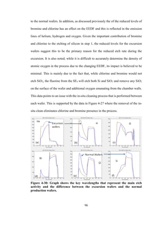
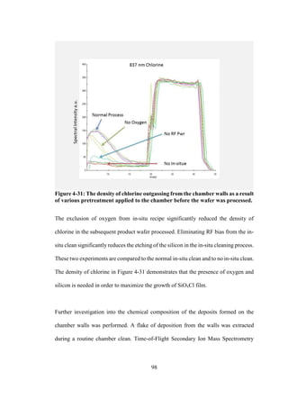
![97
In order to further validate the cause of the lower levels of bromine and chlorine in the
excursion wafers, the in-situ cleaning process was studied. As discussed previously,
the in-situ clean is an Ar/Cl2/HBr/O2 chemistry, with a silicon wafer etching. An RF
bias is also employed to increase the flux and energy of ions to the surface of the wafer
increasing the bombardment of the silicon lattice and thereby enhancing the etching
by chlorine and bromine neutrals. It has been widely reported that the etching of
silicon in the presence of chlorine, bromine and oxygen results in the deposition of
SiOClx and SiOBrx on the chamber walls[16][52][53]. During the in-situ cleaning a
thin layer is deposited on the chamber walls. During the subsequent etching of the
production wafers, the deposited film is etched by the fluorine from the SF6 feed gas
[52]. This liberates chlorine and bromine and oxygen from the film which are then
available to react with the surface of the wafer. From the analysis of the time series
data from chlorine and bromine, it is evident that the densities decreased quickly in
step 1 of the product wafer. This suggests that the film on the chamber wall is thin and
therefore its contribution is limited to the start of the recipe step.
In order to test this hypothesis a number of experiments were conducted in which
processing conditions for the in-situ cleaning were modified. The experimental set up
involved changing a number of recipe parameters in the in-situ clean. The in-situ clean
experiment was followed by a production recipe. OES analysis was then completed
for each of the production recipes to determine the impact the in-situ cleaning had on
each production wafer. In Figure 4-31, chlorine wavelength (837 nm) of the production
process is presented for four adjustments made to the in-situ clean and compared to
the normal in-situ clean.](https://image.slidesharecdn.com/750f8846-02d9-4e6c-84da-231f8478ab05-161124161834/85/NMacgearailt-Sumit_thesis-114-320.jpg)
![102
5 Chapter 5
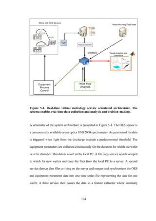
Virtual Metrology in Production
5.1 Introduction
The implementation of virtual metrology in a semiconductor manufacturing can have
significant benefits in terms of cost and quality[54]–[58]. As discussed in the previous
chapter 4, the value virtual metrology can offer goes from simple and accurate
(supervised) fault detection and process diagnostics to enabling metrology reduction
and ultimately process control. The offline analysis of data by an engineer can have
significant benefits in terms of understanding variability within the process and
offering solutions to improving process recipes as well as detecting and diagnosing
process excursions and equipment failures. Implementing this kind of analysis to occur
in real-time with no human intervention and produce reliable and accurate results
presents new challenges. In this chapter the architecture developed to deliver real-time
metrology estimation is discussed. Details of the workflow for the data analysis is also
presented as well as some of the safeguards developed to prevent inaccurate metrology
estimation. Results are presented for the sequential prediction of the etch rate for two
lots before the automated retraining of the model is performed when real metrology is
available for the two lots. A variable contribution pareto algorithm is also discussed in
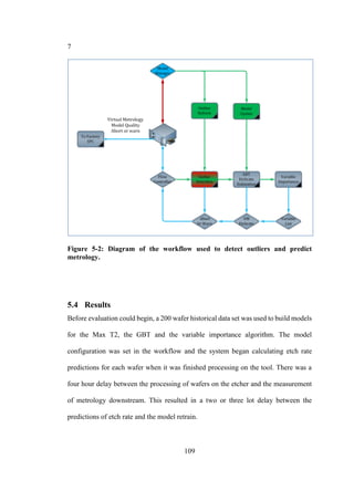
which the variables responsible for the variation in the metrology for each wafer can](https://image.slidesharecdn.com/750f8846-02d9-4e6c-84da-231f8478ab05-161124161834/85/NMacgearailt-Sumit_thesis-119-320.jpg)

![115
limits is considered a fault. This kind of approach generates a lot of false positives and
in some instances false negatives. In some cases, where there have been numerious
alarms an engineer may review the metrology for a period of time and determine a new
good state and recalculate limits. This manual intervention is time-consuming. A
supervised approach to modeling the data is much more effective and accurate and
affords the possibility of a fully automated solution.
In the case study in this chapter, the fully automated architecture and workflow
performed very well in predicting etch rate and providing diagnostic information as to
the cause of the excursions and shifts. The simple outlier detection algorithm detected
the excursion and also provided some warning when there was a shift in the etch rate
but it was still within specifications. The GBT model performed well with the
exception of the first few wafers after the etch rate jump at wafer 900. Here the model
was slow to retrain and alternative approachs could be taken. A number of different
approaches have been explored [59]. Global and local model approaches have been
applied on same dataset as this case study. The best approach for dealing with the
sudden shifts in etch rate were use a short window local model (SWLM). The best
results were achieved in predicting the first few wafers, after a significant etch rate
shift, was to use feature selection and a linear model. Only one wafer after the etch
rate shift was needed in the training dataset to provide accurate prediction of the
subsequent wafers. This approach will be especially useful post maintenance when
chamber conditions are significantly different from a seasoned chamber. The SWLM
approach could be taught on a test wafer post maintenance providing accurate fault](https://image.slidesharecdn.com/750f8846-02d9-4e6c-84da-231f8478ab05-161124161834/85/NMacgearailt-Sumit_thesis-132-320.jpg)
![118
6 Chapter 6
Electrical characterization of a capacitively coupled
plasma etcher.
6.1 Introduction
In the previous chapters, the variation in etch rate was investigated through the analysis
of OES data. It was concluded that the most significant source of variability in the
process came from wall disturbances. In that particular case, the deposition of
SiOxClx[60],[61],[62] on the walls during an in-situ clean resulted in the recycling of
chlorine/bromine and oxygen back into the chamber during normal wafer processing.
The uncontrolled recycling and/or deposition during wafer processing creates
significant wafer to wafer and lot to lot variation in etch performance. The analysis in
the previous chapter 3 only pertained to the data within one maintenance cycle. In
addition to impacting the reproducibility of the plasma process, chamber wall
deposition also generates solid particles. These particles are as a result of thin-film on
the chamber walls flaking off due to stress within the film as well as thermal stresses
induced by turning on and off the RF power. Routine chamber cleaning maintenance
is necessary to keep flaking particles from landing on the surface of the wafer resulting
in defects and impacting yield. During these maintenance cleaning routines chamber
kits, including quartz, stainless steel and ceramics are removed from the chamber and
sent for cleaning. In many instances replacement process chamber kits are installed to](https://image.slidesharecdn.com/750f8846-02d9-4e6c-84da-231f8478ab05-161124161834/85/NMacgearailt-Sumit_thesis-135-320.jpg)
![133
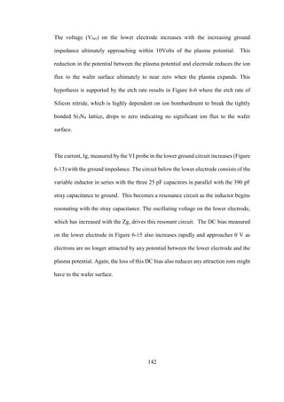
Figure 6-10: Power delivery to the plasma measured at the input to the upper
electrode for a RF setpoint of 300Watts to the RF generator with lower ground
impedance changes.
The RF power is determined by a set point in the process recipe. This signal is relayed
to an RF generator via a 0 to 10 volt analog signal. The RF generator’s on board power
meter ensures that the output power from the generator matches the set point in the
process recipe. Not all the power coming from the RF generator is delivered to the
upper electrode and into the plasma. Some of the power is dissipated in the external
circuitry. These power losses can be large and variable[63][64]. The RF match unit
efficiency varies depending on the operating conditions and the RF current losses. The
matching unit needs to provide equal and opposite impedance to the plasma capacitive
load and maintain a 50 ohm resistive load to the generator. The variable load and
0 20 40 60 80
236
238
240
242
244
246
248
250
252
254
256
258
260
262
PwrUpperElec(Watts)
Z grd ()
Pwr Upper Elec](https://image.slidesharecdn.com/750f8846-02d9-4e6c-84da-231f8478ab05-161124161834/85/NMacgearailt-Sumit_thesis-150-320.jpg)
![134
inductor positions of the match unit change continuously with the different loads
presented by the plasma and chamber. The losses are not linear over the entire range
of the match unit. In addition, other losses associated with the delivery of power to the
upper electrode as well as capacitive leakage to nearby grounding surfaces all
contribute to losses, especially at high voltages. In Figure 6-10 the actual delivered
power measured by the VI probe is displayed as a function of the changing ground
impedance for a fixed 300 W RF setpoint. Losses of up to 50 W are observed.
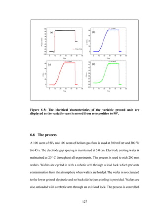
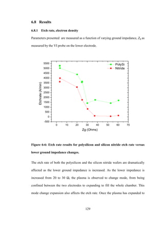
6.8.2 Electrical behaviour of the confined plasma mode
The data in Figure 6-13 shows detailed measurement of the confined stage of the
plasma before expansion to the walls. The etch rate measurements in this experimental
run was limited to polysilicon. As seen before, the etch rate negatively changes as the
lower impedance is increased. The drop in etch rate begins very rapidly after 14 Ω. In
the 0 to 14 Ω region there is little change in etch rate.
In order to explain the behaviour of the discharge in this experiment, a simplified time
average electrical equivalency model was constructed and presented in Figure 6-11.
The electrical characteristics of radiofrequency parallel plate capacitively coupled
discharges have been widely studied both experimentally and theoretically[5], [13],
[65]–[74].](https://image.slidesharecdn.com/750f8846-02d9-4e6c-84da-231f8478ab05-161124161834/85/NMacgearailt-Sumit_thesis-151-320.jpg)
![135
Figure 6-11: Equivalent circuit for simplified electrical model of RF discharge.
A number of assumptions are made as the objective is to capture the basic
characteristics and understand the behaviour of the discharge as the lower impedance
is changed with respect to the impact these have on the etch rate. The plasma sheaths
are considered purely capacitive [70] at 300 mTorr. A number of authors have
considered this approach in modelling the electrical characteristics of the plasma[73].
The resistance of the plasma bulk due to electron-neutral collisions is represented by](https://image.slidesharecdn.com/750f8846-02d9-4e6c-84da-231f8478ab05-161124161834/85/NMacgearailt-Sumit_thesis-152-320.jpg)
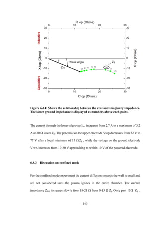
![141
Ztop begins to increase rapidly. When the components of the total impedance Ztop are
looked at individually, the resistive component of the circuit R top is also seen to
increase with Zg. One component of this is a small increases in losses in the lower
grounding unit, while the other component is the ohmic resistance of the plasma bulk.
The imaginary part of the impedance is represented by Xtop. This reactance decreases
from -13 to -9 Ω, the local minimum from where it increases again to-15 Ω. The
sheath impedances are not constant and vary with RF current flow through them[73].
When the plasma starts with the Zg=0, the RF current from the powered electrode
travels the path of least resistance to ground through the plasma bulk resistance and
lower electrode. Some small current will diffuse towards the walls of the chamber.
With no electric potential at the edge to accelerate electrons, the plasma is quenched
at the edges and the lack of charge carriers presents a very high impedance to the
current. As the ground impedance is increased further it forces more of the current to
the walls and increases the plasma’s expansion towards the walls but not all the way
to the walls. This is reflected in the increase in the Real resistance. This confinement
of the plasma is assisted not only by the quenching gas outside the electrode area, but
also the reduction in current (Itop) driven by the higher resistance and the reduction in
Vtop which will affect the electron heating. This regime continues until, finally, so
much current is forced to the walls by the very high impedance of the ground path that
there is enough high energy electrons to create and sustain a discharge all the way to
the walls and the resistance is observed to drop dramatically due to the high availability
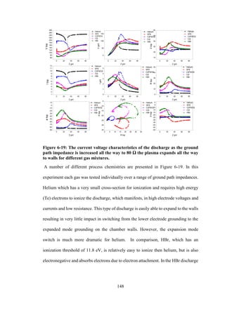
of charge carriers.](https://image.slidesharecdn.com/750f8846-02d9-4e6c-84da-231f8478ab05-161124161834/85/NMacgearailt-Sumit_thesis-158-320.jpg)
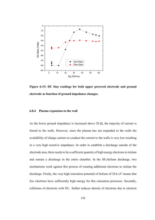
![144
attachment. Both these mechanisms serve to quench the discharge from expanding
beyond the electrode area until electric fields are high enough to sustain high energy
electrons. However, as the voltage in the lower electrode approaches that of the plasma
potential, the electric field gradient shifts away from the lower electrode towards the
walls [75]. This modified electric potential drives more of the current towards the walls
and increases the ionization at the edge of the plasma facilitating the expansion of the
discharge towards the walls. The resultant reduction in resistance facilitates more
current to flow towards the walls allowing the plasma to expand further. This process
reaches a critical point where the specific density and temperature (EEDF) of the
electrons overcomes the loss mechanism and the plasma expands all the way to the
walls. This sudden transition can be clearly seen in the electrical measurements in
Figure 6-16. The reactance Xtop shows the most dramatic shift with a large increase
in impedance from -12 to -18 Ω when the ground impedance reaches 25 Ω. This
dramatic shift occurs because the current has now established a lower resistive path to
ground through the plasma to the walls as opposed to the lower electrode’s circuit. The
inductive component of the lower electrode circuit no longer dominates the imaginary
impedance and its impact in resonating with the capacitance of the sheaths no longer
serves to reduce the overall imaginary impedance. The inclusion of the wall sheath
capacitance in the circuit also serves to drive Xtop lower. This is seen most
predominantly on the Xtop verses Rtop graph in Figure 6-16. The real resistance of
the circuit begins to drop due to the availability of charge carriers in the bulk plasma
which now stretches all the way to the walls, the overall current Itop begins to increase
again.](https://image.slidesharecdn.com/750f8846-02d9-4e6c-84da-231f8478ab05-161124161834/85/NMacgearailt-Sumit_thesis-161-320.jpg)

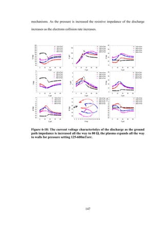
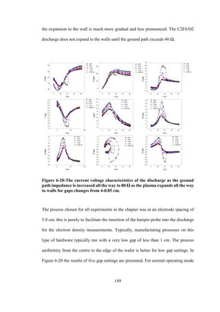
![146
higher power overcomes the quenching mechanisms and hence can strike the discharge
outside of the electrode area [12] more easily.
Figure 6-17: The current voltage characteristics of the discharge as the ground
path impedance is increased all the way to 80 Ω, the plasma expands all the way
to walls for RF power changes from 200-600Watts.
In Figure 6-18 the effect of pressure is displayed. At 125 mTorr the larger mean free
path resulting in higher electron temperature (Te). In this regime the plasma can
expand easily to the walls as the probability of an electron colliding before reaching
the walls is lower, hence, it is able to initiate a discharge outside the electrode area
more effectively. The effect of changing the lower ground impedance at low pressure
is less dramatic than at higher pressures when a plasma is contained by the quenching
0 20 40 60 80
60
80
100
120
140
160
180
200
200 Watts
300 Watts
400 Watts
500 Watts
600 Watts
Vtop
Z grd
0 50 100
2.5
3.0
3.5
4.0
4.5
5.0
5.5
6.0
6.5
7.0
7.5
8.0
8.5
9.0
9.5
10.0
10.5
200 Watts
300 Watts
400 Watts
500 Watts
600 Watts
Itop
Z grd
0 50 100
-80
-60
-40
-20
200 Watts
300 Watts
400 Watts
500 Watts
600 Watts
øtop
Z grd
0 20 40 60 80
0
50
100
150
200 Watts
300 Watts
400 Watts
500 Watts
600 Watts
Vgrd
Z grd
0 20 40 60 80
0.5
1.0
1.5
2.0
2.5
3.0
3.5
4.0
4.5
5.0
5.5 200 Watts
300 Watts
400 Watts
500 Watts
600 Watts
Igrd
Z grd
0 10 20 30
-30
-28
-26
-24
-22
-20
-18
-16
-14
-12
-10 200 Watts
300 Watts
400 Watts
500 Watts
600 Watts
Xtop
R top
0 20 40 60 80
20
30
200 Watts
300 Watts
400 Watts
500 Watts
600 Watts
Ztop
Z grd
0 20 40 60 80
4
6
8
10
12
14
16
18
20
22
24
26 200 Watts
300 Watts
400 Watts
500 Watts
600 Watts
Rtop
Z grd
0 20 40 60 80
-30
-20
-10
200 Watts
300 Watts
400 Watts
500 Watts
600 Watts
Xtop
Z grd](https://image.slidesharecdn.com/750f8846-02d9-4e6c-84da-231f8478ab05-161124161834/85/NMacgearailt-Sumit_thesis-163-320.jpg)
![156
However, there are still a number of key technical challenges that need to be overcome
for large-scale industrial adoption of this technique as an alternative to classical
metrology measurements.
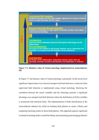
7.2 Equipment hardware diagnostics
Chapter 6 demonstrated the impact that the electrical characteristics of the chamber
hardware can have on the process performance. Maintenance activities in the
semiconductor fab where chambers are disassembled for cleaning have a negative
impact on the repeatability of the process performance. There is a significant risk
associated with performing intrusive but necessary maintenance which can affect the
chamber’s process performance. There is a significant advantage in having electrical
measurements of the process chamber hardware using impedance measurements. The
obvious and most practical measurements involve VI probes or other RF tuning
characteristics which can establish an electrical baseline from which to compare before
and after maintenance. Another approach, not discussed in this thesis investigated was
the use of frequency domain reflectrometry [76]. This technique involves the injection
of a sweeping 100 Hz to 4 GHz signal into the etcher and the measurement of the
reflections. A unique fingerprint of the reflection points of the hardware can be
measured and used to build a baseline. Running argon only discharges can decouple
the complex interactions that electronegative and reactive gases have on the impedance
measurements. This technique has been very successful at generating electrical
fingerprints of the chambers hardware that can be used to evaluate the impact of
maintenance and chamber to chamber matching. The impedances of the chamber with
no plasma (very low RF power) can also be used to baseline the chamber hardware’s
stray impedances.](https://image.slidesharecdn.com/750f8846-02d9-4e6c-84da-231f8478ab05-161124161834/85/NMacgearailt-Sumit_thesis-173-320.jpg)
![157
7.3 Process control- Further work
As the semiconductor process becomes more difficult, even run to run controllers
cannot keep processes on target. The requirement to control the process real-time is
fast becoming a needed reality. The ability to control etch rate in real time using a
predictive control schema was demonstrated to be very effective at mitigating the
effect of disturbances to the RF ground path[77][78]. A virtual metrology model was
used to estimate the etch rate real-time from the VI probe measurements of the plasma.
This data was fed real-time into a control schema which then mitigated any shift in
etch rate by controlling the RF generator’s power output. Disturbances were
introduced by changing the lower ground impedance, as detailed in chapter 6, which
have been shown to have a significant impact on the etch rate. This control schema is
very effective at compensating for these impedance changes on the etch rate by
adjusting the RF power in real-time. These results demonstrate that large disturbances
to the process can be rejected by the controller.
This real-time virtual metrology model does require training over a wide process
parameter space and the sensors need to have very good correlation to the variation in
metrology. This approach offers the ability to retrain the models from production
wafers and improve over time. The control model can react to changes very quickly
and can handle a lot of variation in processing conditions. Additional work would need
to be completed to evaluate this approach and its suitability for high-volume
manufacturing. In particular, the introduction of multiple disturbances, including wall](https://image.slidesharecdn.com/750f8846-02d9-4e6c-84da-231f8478ab05-161124161834/85/NMacgearailt-Sumit_thesis-174-320.jpg)
![158
effects, and how that would impact a controllers ability to keep the etch rate on target
would need to be studied.
A second approach to real time process control is to control the individual plasma
[79]parameters and species densities in real-time. Multivariable closed loop control is
being investigated and has shown very promising results. The real challenge is to adapt
and harden these techniques so that they are robust enough for industrial use.
Appendix I
References
[1] I. Langmuir, “Oscillations in ionized gases,” Phys. Rev., vol. 14, pp. 627–637,
1929.
[2] Michael A. Liebermann; Allan J. Lichtenberg, Principles of plasma
discharges and materials processing. Wiley Interscience.
[3] Robertus Johannes Maria Mathilde Snijkers, “The Sheath of an RF Plasma:
Meauruments and simulations of the ion energy distribution.,” Eindhoven
University of Technology, 1993.
[4] D. Gahan, B. Dolinaj, and M. B. Hopkins, “Retarding field analyzer for ion
energy distribution measurements at a radio-frequency biased electrode.,” Rev.
Sci. Instrum., vol. 79, no. 3, p. 033502, Mar. 2008.](https://image.slidesharecdn.com/750f8846-02d9-4e6c-84da-231f8478ab05-161124161834/85/NMacgearailt-Sumit_thesis-175-320.jpg)
![159
[5] E. Kawamura, A. Wu, M. Lieberman, and A. Lichtenberg, “Stochastic heating
in RF capacitive discharges,” 2006.
[6] M. a. Lieberman and V. a. Godyak, “From Fermi acceleration to collisionless
discharge heating,” IEEE Trans. Plasma Sci., vol. 26, no. 3, pp. 955–986, Jun.
1998.
[7] F. Schulze, “Electron Heating in Capacitively Coupled Radio Frequency
Discharges,” Bochum, 2009.
[8] J. V. Scanlan, “Langmuir probe measurements in 13.56 MHz discharges,”
Dublin City University.
[9] M. Sugawara, Plasma Etching, Fundamentals and Applications. Oxford
University Press, 1998.
[10] B. Chapman, Glow Discharge Processes. John Wiley & Sons, 1980.
[11] A.V. Phelps and L.C. Pitchford, “ELECTRON CROSS SECTIONS,” JILA
Inf. Cent., vol. 26.
[12] Z. Navrátil, P. Dvořák, O. Brzobohatý, and D. Trunec, “Determination of
electron density and temperature in a capacitively coupled RF discharge in
neon by OES complemented with a CR model,” J. Phys. D. Appl. Phys., vol.
43, no. 50, p. 505203, Dec. 2010.
[13] a. J. Lichtenberg, V. Vahedi, M. a. Lieberman, and T. Rognlien, “Modeling
electronegative plasma discharges,” J. Appl. Phys., vol. 75, no. 5, p. 2339,
1994.
[14] M. Turner and M. Hopkins, “Anomalous sheath heating in a low pressure rf
discharge in nitrogen,” Phys. Rev. Lett., vol. 69, no. 24, pp. 3511–3514, 1992.
[15] M. Klick, W. Rehak, and M. Kammeyer, “Plasma diagnostics in rf discharges
using nonlinear and resonance effects,” Japanese J. Appl. …, 1997.
[16] J. Tanaka and G. Miya, “Spatial profile monitoring of etch products of silicon
in HBr∕Cl[sub 2]∕O[sub 2]∕Ar plasma,” J. Vac. Sci. Technol. A Vacuum,
Surfaces, Film., vol. 25, no. 2, p. 353, 2007.
[17] D. Flamm, Mechanisms of silicon etching in fluorine-and chlorine-containing
plasmas, vol. 62, no. 9. 1990, pp. 1709–1720.
[18] D. L. Flamm and V. M. Donnelly, “T h e D e s i g n of P l a s m a E t c h a n t
s Daniel L. Flamm 1 and Vincent M. Donnelly 1,” vol. 1, no. 4, 1981.](https://image.slidesharecdn.com/750f8846-02d9-4e6c-84da-231f8478ab05-161124161834/85/NMacgearailt-Sumit_thesis-176-320.jpg)
![160
[19] S. Sivakumar, “Lithography Challenges for 32nm Technologies and Beyond,”
2006 Int. Electron Devices Meet., pp. 1–4, 2006.
[20] M. El kodadi, S. Soulan, M. Besacier, and P. Schiavone, “Resist trimming
etch process control using dynamic scatterometry,” Microelectron. Eng., vol.
86, no. 4–6, pp. 1040–1042, Apr. 2009.
[21] Y. Zhang, G. S. Oehrlein, and F. H. Bell, “Fluorocarbon high density plasmas
. VII . Investigation of selective SiO 2 -to-Si 3 N 4 high density plasma etch
processes,” vol. 14, no. July 1995, pp. 2127–2137, 1996.
[22] M. Schaepkens and G. S. Oehrlein, “Selective SiO 2 -to-Si 3 N 4 etching in
inductively coupled fluorocarbon plasmas : Angular dependence of SiO 2 and
Si 3 N 4 etching rates,” pp. 3281–3286, 1998.
[23] M. Schaepkens, T. E. F. M. Standaert, N. R. Rueger, P. G. M. Sebel, G. S.
Oehrlein, and J. M. Cook, “Study of the SiO[sub 2]-to-Si[sub 3]N[sub 4] etch
selectivity mechanism in inductively coupled fluorocarbon plasmas and a
comparison with the SiO[sub 2]-to-Si mechanism,” J. Vac. Sci. Technol. A
Vacuum, Surfaces, Film., vol. 17, no. 1, p. 26, 1999.
[24] L. Chen, L. Xu, D. Li, and B. Lin, “Mechanism of selective Si3N4 etching
over SiO2 in hydrogen-containing fluorocarbon plasma,” Microelectron. Eng.,
vol. 86, no. 11, pp. 2354–2357, Nov. 2009.
[25] M. Matsui, T. Tatsumi, and M. Sekine, “Relationship of etch reaction and
reactive species flux in C[sub 4]F[sub 8]/Ar/O[sub 2] plasma for SiO[sub 2]
selective etching over Si and Si[sub 3]N[sub 4],” J. Vac. Sci. Technol. A
Vacuum, Surfaces, Film., vol. 19, no. 5, p. 2089, 2001.
[26] R. Westerman and D. Johnson, “Endpoint detection methods for time division
multiplex etch processes,” … 2006 Micro …, 2006.
[27] N. MacGearailt, “Endpoint via NMACG.” 1998.
[28] M. Darnon, C. Petit-Etienne, and E. Pargon, “Synchronous Pulsed Plasma for
Silicon Etch Applications,” ECS …, vol. 27, no. 1, pp. 717–723, 2010.
[29] J. P. Chang and H. H. Sawin, “Notch formation by stress enhanced
spontaneous etching of polysilicon,” J. Vac. Sci. Technol. B Microelectron.
Nanom. Struct., vol. 19, no. 5, p. 1870, 2001.
[30] H. G. Kosmahl, “Plasma Acceleration with Microwaves near Cyclotron
Resonance,” J. Appl. Phys., vol. 38, no. 12, p. 4576, 1967.
[31] K. Suzuki and S. Okudaira, “Microwave plasma etching,” Japanese J. …,
1977.](https://image.slidesharecdn.com/750f8846-02d9-4e6c-84da-231f8478ab05-161124161834/85/NMacgearailt-Sumit_thesis-177-320.jpg)
![161
[32] “Radar Recollections.” [Online]. Available:
http://histru.bournemouth.ac.uk/Oral_History/Talking_About_Technology/rad
ar_research/the_magnetron.html.
[33] “Magnetron Theory of Operation,” Division, Beverly Microwaver. [Online].
Available: http://www.cpii.com/.
[34] “Magnetrons Cross Section.” [Online]. Available:
http://microwavetubes.iwarp.com/How_Magnetron_Work.html.
[35] Y. Yoshizako, M. Taniguchi, and Y. Ishida, “Microwave power source
apparatus for microwave oscillator comprising means for automatically
adjusting progressive wave power and control method therefor,” US Pat.
5,399,977, 1995.
[36] O. A. Popov and J. E. Stevens, High Density Plasma Sources. 1996.
[37] R. Kinder and M. Kushner, “Consequences of mode structure on plasma
properties in electron cyclotron resonance sources,” J. Vac. Sci. Technol. A
Vacuum, …, no. January, pp. 2421–2430, 1999.
[38] N. Carolina, R. L. Kinder, and M. J. Kushner, “SIMULATIONS OF ECR
PROCESSING SYSTEMS SUSTAINED BY AZIMUTHAL MICROWAVE
TE ( 0 , n ) MODES *,” 1998.
[39] “Semiconductor Equipment and Materials International.” [Online]. Available:
http://www.semi.org.
[40] N. MacGearailt, “Endpoint of <0.5 % open area with a VI sensor.”
[41] N. Dewan, “Analysis and modelling of the impact of plasma RF harmonics in
semiconductor plasma processing,” Dublin City University, 2001.
[42] R. L. Stenzel, “Microwave resonator probe for localized density
measurements in weakly magnetized plasmas,” Rev. Sci. Instrum., vol. 47, no.
5, p. 603, 1976.
[43] Campbel N.A. and Atchley W.R., The geometry of canonical variate analysis.
Syst. Zool, 1981.
[44] “PCA Diagram.” [Online]. Available:
http://web.media.mit.edu/~tristan/phd/dissertation/chapter5.html.
[45] “No Title.” [Online]. Available: http://umetrics.com/.
[46] J. E. Jackson, A Users Guide to principle components. Wiley Interscience,
1991.](https://image.slidesharecdn.com/750f8846-02d9-4e6c-84da-231f8478ab05-161124161834/85/NMacgearailt-Sumit_thesis-178-320.jpg)
![162
[47] “Private Correspondance with Dr. Eugene Tuv.” .
[48] M. M. Turner, “Actinometry - Use of Particle In Cell code to generate
improved rate constants for determination of absolute O,” pp. 1–11.
[49] H. M. Katsch, A. Tewes, E. Quandt, A. Goehlich, and T. Kawetzki,
“Detection of atomic oxygen : Improvement of actinometry and comparison
with laser spectroscopy Detection of atomic oxygen : Improvement of
actinometry and comparison with laser spectroscopy,” vol. 6232, 2000.
[50] E. de la Cal, D. Tafalla, and F. L. Tabares, “Characterization of He/CH4 dc
glow discharge plasmas by optical emission spectroscopy, mass spectrometry,
and actinometry,” J. Appl. Phys., vol. 73, no. 2, p. 948, 1993.
[51] “National Institute of Standards and Technology Atomic Spectra Database.” .
[52] a. Le Gouil, E. Pargon, G. Cunge, O. Joubert, and B. Pelissier, “Chemical
analysis of deposits formed on the reactor walls during silicon and metal gate
etching processes,” J. Vac. Sci. Technol. B Microelectron. Nanom. Struct., vol.
24, no. 5, p. 2191, 2006.
[53] S. Bouchoule, L. Vallier, G. Patriarche, T. Chevolleau, and C. Cardinaud,
“Effect of Cl2- and HBr-based inductively coupled plasma etching on InP
surface composition analyzed using in situ x-ray photoelectron spectroscopy,”
J. Vac. Sci. Technol. A Vacuum, Surfaces, Film., vol. 30, no. 3, p. 031301,
2012.
[54] F. Cheng, “Design and Implementation of a Virtual Metrology System,” 2005.
[55] S. Wu, F. Ko, H. Lo, J. Wang, C. H. Yu, and M. S. Liang, “Virtual metrology:
a solution for wafer to wafer advanced process control,” ISSM 2005, IEEE Int.
Symp. Semicond. Manuf. 2005., pp. 155–157, 2005.
[56] T. Wünsche, M. Rudolph, and J. Zimpel, “Virtual Metrology to Measure Mass
Loss at Deep Trench Processes Motivation to Measure the Mass Loss during
the Deep Trench Etch Process,” 2007.
[57] F. Y. Wang, “Virtual Metrology — A Solution for Wafer to Wafer Process
Monitoring And Throughput Enhancement,” pp. 1–12.
[58] T. Lin, M. Hung, R. Lin, and F. Cheng, “A Virtual Metrology Scheme for
Predicting CVD Thickness in,” no. May, pp. 1054–1059, 2006.
[59] N. M. E Ragnoli (NUIM Maynooth, N MacGearailt, Intel Ireland, Sean
Mcclone, “EmanueleRagnoliIntelConference2009.” 2009.](https://image.slidesharecdn.com/750f8846-02d9-4e6c-84da-231f8478ab05-161124161834/85/NMacgearailt-Sumit_thesis-179-320.jpg)
![163
[60] T. W. Kim and E. S. Aydil, “Effects of Chamber Wall Conditions on Cl
Concentration and Si Etch Rate Uniformity in Plasma Etching Reactors,” J.
Electrochem. Soc., vol. 150, no. 7, p. G418, 2003.
[61] M. Kogelschatz, G. Cunge, N. Sadeghi, and O. Joubert, “Characterisation of
layers deposited on reactor walls by plasma etching,” no. Lam 9400, pp. 130–
134.
[62] G. Cunge, B. Pelissier, O. Joubert, R. Ramos, and C. Maurice, “New chamber
walls conditioning and cleaning strategies to improve the stability of plasma
processes,” Plasma Sources Sci. Technol., vol. 14, no. 3, pp. 599–609, Aug.
2005.
[63] F. Bose, “Characterization of plasma etch processes using measurements of
discharge impedance,” J. Vac. Sci. Technol. B Microelectron. Nanom. Struct.,
vol. 12, no. 4, p. 2805, Jul. 1994.
[64] J. G. Langan, S. E. Beck, B. S. Felker, and S. W. Rynders, “The role of
diluents in electronegative fluorinated gas discharges,” J. Appl. Phys., vol. 79,
no. 8, p. 3886, 1996.
[65] B. Andries, “Electrical characterization of radio-frequency parallel-plate
capacitively coupled discharges,” J. Vac. Sci. Technol. A Vacuum, Surfaces,
Film., vol. 7, no. 4, p. 2774, Jul. 1989.
[66] E. At, “Detailed Investigations of the Sheath Dynamics and Elementary
Processes in Capacitively Coupled RF Plasmas Inauguraldissertation,” no.
September 1980, 2009.
[67] V. A. Godyak, “Dynamic model of the electrode sheaths in symmetrically,”
vol. 42, no. 4, 1990.
[68] M. Grapperhaus and M. Kushner, “A semianalytic radio frequency sheath
model integrated into a two-dimensional hybrid model for plasma processing
reactors,” J. Appl. Phys., vol. 81, no. January, pp. 569–577, 1997.
[69] H. R. Koenig and L. I. Maissel, “Application of rf discharges to sputtering,”
IBM J. Res. Dev., vol. 44, no. 1.2, pp. 106–110, Jan. 2000.
[70] K. Köhler, J. W. Coburn, D. E. Horne, E. Kay, and J. H. Keller, “Plasma
potentials of 13.56-MHz rf argon glow discharges in a planar system,” J. Appl.
Phys., vol. 57, no. 1, p. 59, 1985.
[71] Y. D. Lee and J. J. Oh, “Dynamic model and electrical characteristics for rf-
biased electronegative plasma sheath,” IEEE Trans. Plasma Sci., vol. 30, no.
3, pp. 1320–1330, Jun. 2002.](https://image.slidesharecdn.com/750f8846-02d9-4e6c-84da-231f8478ab05-161124161834/85/NMacgearailt-Sumit_thesis-180-320.jpg)
![164
[72] M. Lieberman, “Analytical solution for capacitive RF sheath,” Plasma Sci.
IEEE Trans., vol. 16, no. 6, pp. 638–644, 1988.
[73] J. S. Logan, “Control of RF Sputtered Film Properties,” IBM J. Res. Dev., vol.
14, no. 2, p. 172, 1970.
[74] M. a. Sobolewski, “Electrical optimization of plasma-enhanced chemical
vapor deposition chamber cleaning plasmas,” J. Vac. Sci. Technol. B
Microelectron. Nanom. Struct., vol. 16, no. 1, p. 173, Jan. 1998.
[75] K. L. Steffens and M. a. Sobolewski, “Planar laser-induced fluorescence of
CF[sub 2] in O[sub 2]/CF[sub 4] and O[sub 2]/C[sub 2]F[sub 6] chamber-
cleaning plasmas: Spatial uniformity and comparison to electrical
measurements,” J. Vac. Sci. Technol. A Vacuum, Surfaces, Film., vol. 17, no.
2, p. 517, 1999.
[76] V. J. Law and N. Macgearailt, “Frequency domain reflectometry of Hitachi
ECR plasma-tool ELECTRONICS LETTERS 5th January 2006,” vol. 42, no.
1, pp. 0–1, 2006.
[77] S. Lynn, N. MacGearailt, and J. Ringwood, “Real-time virtual metrology and
control for plasma etch,” J. Process Control, 2012.
[78] MacGearailt, “Opportunities for APC/AEC in 450mm and beyond.” APC
Conference 2012 Grenoble, 2012.
[79] D. B.J. Keville,Y. Zhang,M. Turner, “Multivariable Control of a Capacitively
Coupled Plasma.”](https://image.slidesharecdn.com/750f8846-02d9-4e6c-84da-231f8478ab05-161124161834/85/NMacgearailt-Sumit_thesis-181-320.jpg)