![Atif Syed
Nanofabrication
2
1. Introduction:
One of the fastest growing markets in consumer electronics is the Flat Panel Displays
(FPDs). The market value for FPD in 1999 was estimated to be around 18.5 billion dollars
and it was predicted to reach $70 billion by 2010 which would surpass the production of
CRTs by a huge margin [1]. There are many different types of FPD such as LCD, TFT,
Plasma and Projection Displays which can be found in the market. This report will focus
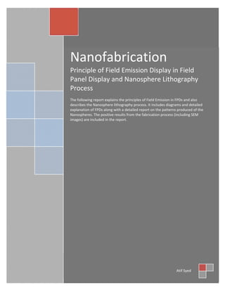
on one such technology known as the Field Emission Display (FED). A basic flow chart for
display fabrication process is given below:
Figure 1.1: Display Fabrication flowchart
The information display has always been a very critical human interface with the
computer/electronic systems. FPD’s allows us to produce HDTV at an affordable cost.
One of the most prominent features of FPD is that each pixel generates its own light
energy which allows the display to have high resolution.
Cathode
Fabrication
Grid
Attachment
Spacer
Placement
Vacuum
Seal
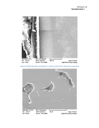
Anode
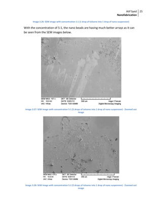
Fabrication
Sidewall
Attachment
Getter
Attachment
Tip off and
gettering](https://image.slidesharecdn.com/nanofab-atifsyed-130430122123-phpapp02/85/Nanofabrication-2-320.jpg)
![Atif Syed
Nanofabrication
3
2. Principle and Working of FED:
FEDs work on the similar principle of the Cathode Ray Tube (CRTs) and Vacuum
Fluorescent Display (VFD) where an electron gun is used with high voltage of up to 10‐
30 kV which accelerates the electrons and those electrons excite phosphors. The only
difference in FED is that instead of a single electron gun, there is a matrix‐addressed
array of millions of cold emitters [1]. These arrays in short are known as the Field
Emission Array (FEA). These arrays are arranged in a very close proximity usually around
0.2‐2.0 mm to a phosphor faceplate 1
(Anode) so that each phosphor pixel has individual
or dedicated field emitters. FEDs consist of hermetically2
sealed glass envelope which is
evacuated to form a vacuum space which allows the electrons beam to accelerate [2]. In
addition to the faceplate, a back‐plate (Cathode or source of electrons), sidewalls,
spacers and getters are also used in the working of FEDs. The anode and cathode are
fabricated separately as described in Figure 1. The metallic stripes on the faceplate form
a series of cathode lines and by the process of Photolithography, the cathode lines are
fabricated in such a way that they are arranged at 90 degree angles which forms rows of
switching gates and these arrays form a perfect addressable grid. After the
Photolithography process, the grid can be addressed individually and the emitters in
between the cathode and anode/gate lines will have enough power to produce a visible
spot and all other leakage will not be visible due to high power of illumination of the
visible spot.
Figure 2.1: Field Emission Working Principle Diagram
1
Generally Faceplate is a type of metal or plastic plate which is designed to cover or fit on a device or a
component to enhance the device’s functionality or its appearance. In this context it’s referring Anode.
2
Completely sealed or air tight so that the interior/material is not affected by outside influence.
Anode Plate
Cathode Plate
Phosphor Dots
Spacer
Electrons
Anode
Addressing
Gate
Addressing
Cathode
Addressing
Interlayer
Dielectric
MicroTip
Emitters](https://image.slidesharecdn.com/nanofab-atifsyed-130430122123-phpapp02/85/Nanofabrication-3-320.jpg)
![Atif Syed
Nanofabrication
4
The first step of the working of Field Emission is done by emitting electrons parallel to
the cathode in between the space which contains ceramic spacers and they withstand
any atmospheric pressure changes and adding ceramic spacers reduces the structure
from collapsing. These spaces should also be able to withstand high voltage and should
be invincible to users at normal viewing range. The electrode gap which is about few
nanometers in length is still is a vacuum gap which required an electric potential to
extract electrons from one electrode to other electrode in other words from cathode to
anode. The electrons which are emitted from cathode are sent directly to the anode but
one has to be careful to block the electrons from striking other surface apart from
anode because this will lead to dead pixels. The current flow within the electrode gap
follows Nordheim Law which determines the emitted current density in its simplest
approximation and it’s given by the following equation [3]:
/
Equation 1
Where is the surface electric filed, B is the emitting material, J is the current density
and is the initial surface electric field when the electric field is 0.
With the help of Nordheim Law the addressability of the matrix is determined even with
the emission being non linear in nature.
Secondly, the electrons travel across the gap and the flow of electrons is from cathode
to anode which in turn is accelerated to a single phosphor dot. This creates the three
basic colors Red,Green and Blue. This can be further explained through the figure below:
Va
Figure 3.1: Tunneling of Electrons across the nano gap
Electric Field
Carbon Nano gap
Vf
Upward Force
Equi‐Potential
lf
le](https://image.slidesharecdn.com/nanofab-atifsyed-130430122123-phpapp02/85/Nanofabrication-4-320.jpg)
![Atif Syed
Nanofabrication
5
In figure 3, Va is the anode potential and Vf is the driving potential across the gap. The
electrons might scatter a lot of times before actually getting captured by the anode. The
efficiency of the captured electrons is given by (le/lf) and for typical FPD it comes to
around 3% [2] and this is very low. Although the power efficiency is acceptable because
Vf is low this is normally at 20V. If Vf is high the efficiency is reduced according to
Nordheim Law which is also a determining factor for the uniformity of electron current
actually reaching the anode. Nordheim Law is applied to the scattering events of
electrons from pixel to pixel and the closest approximation is taken according to the
Equation 1.
The emitters as described in Figure 3 are fabricated by using a printing method. This is
achieved by directly printing the silver wires at the crossovers. Usually Platinum (Pt)
electrodes are formed through thin‐film lithography process. The carbon‐nano gap as
mentioned in Figure 3 is done through 2 step fabrication process. There are many ways
to achieve this but one of it is done by depositing a film of Palladium Oxide (PdO)
through the Printing method. The gap is actually formed by reducing the oxide. The
oxide is reduced by giving a series of voltage pulses across the PdO film which is
sandwiched between the cathode and anode. While reducing the PdO, the film is
eventually transformed into a sub‐micron gap which forms a PdO dot. The gap is then
activated by exposing cathode to organic gas and more voltage pulses are provided
across the gap. When the gap becomes smaller in size, the pulse becomes larger and
eventually the material is evaporated.
In anode fabrication process a black matrix and color filters are used. The color filters
are used to increase the contrast and the metallic black matrix is used to increase the
brightness. The cold emitters are deposited at the intersection of each row. In between
the emitters and metallic mesh, a high voltage field is created which in turn pulls the
electrons from the tip of the emitters. Since this process is non linear, a small change in
the voltage will cause the emitted electrons to saturate. Due to the non linearity, once
the pixels are lit up, the visible light stays for a while. To maintain emission uniformity
within the pixels usually a current feedback resistor is placed in series with the cathode
electrode [2]. Typically FEDs are voltage driven devices where it is difficult to apply more
than 2‐3 voltage levels in between cathode and the gates. To avoid this, a gray scale
image is achieved by the principle of Pulse Width Modulation which allows to control
the power of transmission and in this case controlling the number of electrons produced
[2]. For all other passive matrix FPD, the image is created line by line where just one line
is activated and the pixels are illuminated by the column drivers. The illuminating period
is determined by the intensity which is required for the pixel in that particular image
frame.](https://image.slidesharecdn.com/nanofab-atifsyed-130430122123-phpapp02/85/Nanofabrication-5-320.jpg)
![Atif Syed
Nanofabrication
6
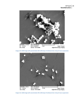
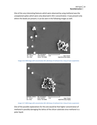
3. Nano sphere lithography process:
The process was carried out with the described method in the lab script. Although
the method was followed as said but there were experiments done with different
chemicals and concentrations. This section will explain each chemical used which is
followed by the SEM images before and after the evaporation step.
The first and second steps are common for all the chemicals used. The steps and
results are given below:
‐ Step 1: The silicon wafer of <100> has been cut carefully in a square of 1cm
dimension.
‐ Step 2: The samples of silicon wafers are then are held over boiling acetone and
propan‐2‐ol. The samples are then kept in a beaker and agitated in the ultrasonic
cleaner for an hour. These samples are then kept under water so that it can be
hydrophilic3
.
‐ Step 3: Polystyrene Nanosphere suspension has been used with a suspension of
0.8 micron Nanospheres (as opposed to 0.52 microns mentioned in the lab
script. The reason behind this is that the Nanospheres were too small to be
viewed clearly through the SEM).
The above steps are common for all the chemicals used. The following chemicals and
solutions were used in the experiments:
De‐ionized water
Ammonia ( )
Methanol ( )
Toluene ( ) [This is a substitute to Benzene]
The remaining steps of the preparation of the nano beads with the chemicals mentioned
above will be explained in details with the results and comments. The next sub‐section
3
The hydrophilic property has been experimented with different chemicals explained later in the report.
It has been done to further investigate the possibility of making better nano sphere arrays and also by
making the surface tension minimum or low enough to make a perfect array.](https://image.slidesharecdn.com/nanofab-atifsyed-130430122123-phpapp02/85/Nanofabrication-6-320.jpg)


![Atif Syed
Nanofabrication
39
Major problems faced during the experiment:
‐ During evaporation, the substrates which were stuck on the glass slab fell off and
some were hanging in the chamber and some samples didn’t had the
evaporation done properly, the vertical evaporation can be seen in the following
image of toluene sample. Due to this not all the evaporated samples were
annealed.
Image 3.54: SEM image with concentration 1:1 after annealing (1 drop of toluene into 1 drop of nano suspension)
‐ The clean room atmosphere had dirt and dust which can be clearly seen in the
SEM images of the samples.
‐ The heating plate during the annealing process didn’t allowed the samples to be
annealed at a temperature more than 550 C despite the fact that the results are
proven to be better at temperatures more than 750 C [4] [5] and the Low‐
Pressure Chemical‐Vapor‐deposited (LPCVD) oxide thermal conductivity
increases by 23% at 1150 C [6].
‐ If the experiment was carried out with no interference with the samples
(including people moving the samples while the samples are drying), much
better results could have been achieved.](https://image.slidesharecdn.com/nanofab-atifsyed-130430122123-phpapp02/85/Nanofabrication-39-320.jpg)
![Atif Syed
Nanofabrication
40
References
[1] A.A Talin, K.A Dean, J.E Jaskie, "Field Emission Dsiplays," 2011.
[2] Richard Fink, Zvi Yanib, "A closer look at SED, FED technologies".
[3] YY Lau, Youfan Liu, RK Parker, "Electron Emision: From the Fowler‐Bordheim relation to the
Langmuir Law".
[4] D. Lysáček, L. Válek, "Structural changes of polycrystalline silicon layers during high
temperature annealing".
[5] Hatalis, Miltiadis K.; Greve, David W., "Large grain polycrystalline silicon by low‐
temperature annealing of low‐pressure chemical vapor deposited amorphous silicon films,"
Journal of Applied Physics, vol. 63, pp. 2260‐2266.
[6] K. E. Goodson, M. I. Flik, L. T. Su, Dimitri A. Antoniadis , "Annealing‐Temperature
Dependence of the Thermal Conductivity of LPCVD Silicon‐Dioxide Layers," IEEE ELECTRON
DEVICE L E T E R S, vol. 14, no. 10, 1993.](https://image.slidesharecdn.com/nanofab-atifsyed-130430122123-phpapp02/85/Nanofabrication-40-320.jpg)

Field emission displays (FEDs) work by using cold emitter arrays to emit electrons that excite phosphors on an anode, producing pixels. Nanosphere lithography involves self-assembling nanospheres onto a substrate to act as a mask for depositing materials underneath. The report describes the FED working principle, fabrication process, and experimental results using nanosphere lithography with different chemicals to pattern silicon wafers. SEM images show the patterned structures produced before and after material evaporation.


