Materials For Solid State Lighting And Displays Kitai Adrian
Materials For Solid State Lighting And Displays Kitai Adrian
Materials For Solid State Lighting And Displays Kitai Adrian
Materials For Solid State Lighting And Displays Kitai Adrian
Materials For Solid State Lighting And Displays Kitai Adrian
1.
Materials For SolidState Lighting And Displays
Kitai Adrian download
https://ebookbell.com/product/materials-for-solid-state-lighting-
and-displays-kitai-adrian-6755056
Explore and download more ebooks at ebookbell.com
2.
Here are somerecommended products that we believe you will be
interested in. You can click the link to download.
Negative Electrode Materials For Lithiumion Solidstate Microbatteries
Loc Baggetto
https://ebookbell.com/product/negative-electrode-materials-for-
lithiumion-solidstate-microbatteries-loc-baggetto-6101804
Optical Techniques For Solidstate Materials Characterization Rohit P
Prasankumar Antoinette J Taylor
https://ebookbell.com/product/optical-techniques-for-solidstate-
materials-characterization-rohit-p-prasankumar-antoinette-j-
taylor-4393816
Solidstate Lasers For Materials Processing Fundamental Relations And
Technical Realizations 1st Edition Reinhard Ifflnder Diplphys Auth
https://ebookbell.com/product/solidstate-lasers-for-materials-
processing-fundamental-relations-and-technical-realizations-1st-
edition-reinhard-ifflnder-diplphys-auth-4187374
Computational Chemistry Of Solid State Materials A Guide For Materials
Scientists Chemists Physicists And Others 1st Edition Richard
Dronskowski
https://ebookbell.com/product/computational-chemistry-of-solid-state-
materials-a-guide-for-materials-scientists-chemists-physicists-and-
others-1st-edition-richard-dronskowski-1406060
3.
Midsize Facilities TheInfrastructure For Materials Research 1st
Edition National Research Council Division On Engineering And Physical
Sciences Board On Physics And Astronomy Solid State Sciences Committee
Committee On Smaller Facilities
https://ebookbell.com/product/midsize-facilities-the-infrastructure-
for-materials-research-1st-edition-national-research-council-division-
on-engineering-and-physical-sciences-board-on-physics-and-astronomy-
solid-state-sciences-committee-committee-on-smaller-
facilities-51594910
Solid Wastebased Materials For Environmental Remediation Guanyi Chen
https://ebookbell.com/product/solid-wastebased-materials-for-
environmental-remediation-guanyi-chen-61398200
Mechanical Vibration Methods For Studying Physical Properties Of Solid
Materials 1st Edition Y Hiki
https://ebookbell.com/product/mechanical-vibration-methods-for-
studying-physical-properties-of-solid-materials-1st-edition-y-
hiki-51357034
Novel Cobaltfree Perovskite Prbafe19mo01o5 As A Cathode Material For
Solid Oxide Fuel Cells Haixia Zhang
https://ebookbell.com/product/novel-cobaltfree-perovskite-
prbafe19mo01o5-as-a-cathode-material-for-solid-oxide-fuel-cells-
haixia-zhang-48498106
Material And Energy Recovery From Solid Waste For A Circular Economy
Atun Roy Choudhury Sankar Ganesh Palani
https://ebookbell.com/product/material-and-energy-recovery-from-solid-
waste-for-a-circular-economy-atun-roy-choudhury-sankar-ganesh-
palani-57657064
Wiley Series inMaterials for Electronic and Optoelectronic Applications
www.wiley.com/go/meoa
Series Editors
Professor Arthur Willoughby, University of Southampton, Southampton, UK
Dr Peter Capper, formerly of SELEX Galileo Infrared Ltd, Southampton, UK
Professor Safa Kasap, University of Saskatchewan, Saskatoon, Canada
Published Titles
Bulk Crystal Growth of Electronic, Optical and Optoelectronic Materials, Edited by
P. Capper
Properties of Group-IV, III–V and II–VI Semiconductors, S. Adachi
Charge Transport in Disordered Solids with Applications in Electronics, Edited by
S. Baranovski
Optical Properties of Condensed Matter and Applications, Edited by J. Singh
Thin Film Solar Cells: Fabrication, Characterization, and Applications, Edited by
J. Poortmans and V. Arkhipov
Dielectric Films for Advanced Microelectronics, Edited by M. R. Baklanov, M. Green, and
K. Maex
Liquid Phase Epitaxy of Electronic, Optical and Optoelectronic Materials, Edited by
P. Capper and M. Mauk
Molecular Electronics: From Principles to Practice, M. Petty
CVD Diamond for Electronic Devices and Sensors, Edited by R. S. Sussmann
Properties of Semiconductor Alloys: Group-IV, III–V, and II–VI Semiconductors,
S. Adachi
Mercury Cadmium Telluride, Edited by P. Capper and J. Garland
Zinc Oxide Materials for Electronic and Optoelectronic Device Applications, Edited by
C. Litton, D. C. Reynolds, and T. C. Collins
Lead-Free Solders: Materials Reliability for Electronics, Edited by K. N. Subramanian
Silicon Photonics: Fundamentals and Devices, M. Jamal Deen and P. K. Basu
Nanostructured and Subwavelength Waveguides: Fundamentals and Applications,
M. Skorobogatiy
Photovoltaic Materials: From Crystalline Silicon to Third-Generation Approaches,
G. Conibeer and A. Willoughby
Glancing Angle Deposition of Thin Films: Engineering the Nanoscale, Matthew
M. Hawkeye, Michael T. Taschuk and Michael J. Brett
Spintronics for Next Generation Innovative Devices, Edited by Katsuaki Sato and
Eiji Saitoh
Physical Properties of High-Temperature Superconductors, Rainer Wesche
Inorganic Glasses for Photonics, Animesh Jha
Amorphous Semiconductors: Structural, Optical and Electronic Properties, Koichi
Shimakawa, Sandor Kugler and Kazuo Morigaki
7.
Materials for SolidState
Lighting and Displays
Edited by
ADRIAN KITAI
Departments of Engineering Physics and Materials Science and
Engineering, McMaster University, Hamilton, Canada
Contents
List of Contributorsxi
Series Preface xiii
Preface xv
Acknowledgments xvii
About the Editor xix
1. Principles of Solid State Luminescence 1
Adrian Kitai
1.1 Introduction to Radiation from an Accelerating Charge 1
1.2 Radiation from an Oscillating Dipole 4
1.3 Quantum Description of an Electron during a Radiation Event 5
1.4 The Exciton 7
1.5 Two-Electron Atoms 10
1.6 Molecular Excitons 16
1.7 Band-to-Band Transitions 19
1.8 Photometric Units 23
1.9 The Light Emitting Diode 28
References 30
2. Quantum Dots for Displays and Solid State Lighting 31
Jesse R. Manders, Debasis Bera, Lei Qian and Paul H. Holloway
2.1 Introduction 31
2.2 Nanostructured Materials 34
2.3 Quantum Dots 35
2.3.1 History of Quantum Dots 36
2.3.2 Structure and Properties Relationship 36
2.3.3 Quantum Confinement Effects on Band Gap 38
2.4 Relaxation Process of Excitons 41
2.4.1 Radiative Relaxation 42
2.4.2 Nonradiative Relaxation Process 45
2.5 Blinking Effect 46
2.6 Surface Passivation 47
2.6.1 Organically Capped QDs 47
2.6.2 Inorganically Passivated QDs 48
10.
vi Contents
2.7 SynthesisProcesses 49
2.7.1 Top-Down Synthesis 49
2.7.2 Bottom-Up Approach 50
2.8 Optical Properties and Applications 53
2.8.1 Displays 53
2.8.2 Solid State Lighting 73
2.8.3 Biological Applications 78
2.9 Perspective 81
Acknowledgments 82
References 82
3. Color Conversion Phosphors for Light Emitting Diodes 91
Jack Silver, George R. Fern and Robert Withnall
3.1 Introduction 91
3.2 Disadvantages of Using LEDs Without Color Conversion Phosphors 93
3.3 Phosphors for Converting the Color of Light Emitted by LEDs 95
3.3.1 General Considerations 95
3.3.2 Requirements of Color Conversion Phosphors 95
3.3.3 Commonly Used Activators in Color Conversion Phosphors 97
3.3.4 Strategies for Generating White Light from LEDs 97
3.3.5 Outstanding Problems with Color Conversion Phosphors for
LEDs 98
3.4 Survey of the Synthesis and Properties of Some Currently Available
Color Conversion Phosphors 99
3.4.1 Phosphor synthesis 99
3.4.2 Metal Oxide Based Phosphors 99
3.4.3 Metal Sulfide Based Phosphors 113
3.4.4 Metal Nitrides 117
3.4.5 Alkaline Earth Metal Oxo-Nitrides 120
3.4.6 Metal Fluoride Phosphors 121
3.5 Multi-Phosphor pcLEDs 122
3.6 Quantum Dots 123
3.7 Laser Diodes 124
3.8 Conclusions 125
Acknowledgments 125
References 126
4. Nitride and Oxynitride Phosphors for Light Emitting Diodes 135
Le Wang and Rong-Jun Xie
4.1 Introduction 135
4.2 Synthesis of Nitride and Oxynitride Phosphors 138
4.2.1 Solid State Reaction Method 138
4.2.2 Gas Reduction and Nitridation 139
4.2.3 Carbothermal Reduction and Nitridation 140
4.2.4 Alloy Nitridation 140
4.2.5 Ammonothermal Synthesis 141
11.
Contents vii
4.3 PhotoluminescenceProperties of Nitride and Oxynitride Phosphors 142
4.3.1 Luminescence Spectra of Typical Activators 142
4.4 Emerging Nitride Phosphors and Their Synthesis 165
4.4.1 Narrow-Band Red Nitride Phosphors 165
4.4.2 Narrow-Band Green Nitride Phosphors 167
4.5 Applications of Nitride Phosphors 169
4.5.1 General Lighting 169
4.5.2 LCD Backlight 172
References 173
5. Organic Light Emitting Device Materials for Displays 183
Tyler Davidson-Hall, Yoshitaka Kajiyama and Hany Aziz
5.1 Introduction to OLEDs and Organic Electroluminscent Materials 184
5.2 OLED Light Emitting Materials 186
5.2.1 Neat Emitters 187
5.2.2 Guest Emitters 192
5.2.3 Aggregate-Induced Emission 201
5.3 OLED Displays 203
5.3.1 RGB Color Patterning Approaches 203
5.3.2 Display Addressing Approaches 204
5.3.3 FMM Technology 207
5.3.4 Alternative Fabrication Techniques 208
5.3.5 Outlook on OLED Display Commercialization 212
5.4 Quantum Dot Light Emitting Devices 213
5.4.1 QD Optimization by Core–Shell Morphology 214
5.4.2 Organic Charge Transport QD-LEDs 215
5.4.3 Hybrid Organic–Inorganic Charge Transport QD-LEDs 217
5.4.4 Energy Transfer Enhanced QD-LEDs 219
5.4.5 QD-LED Lifetime 220
References 220
6. White-Light Emitting Materials for Organic Light-Emitting Diode-Based
Displays and Lighting 231
Simone Lenk, Michael Thomschke and Sebastian Reineke
6.1 Introduction 231
6.2 White Organic Light-Emitting Diodes 233
6.3 Photometry and Radiometry 236
6.3.1 OLED Efficiencies 239
6.3.2 Color Stimulus Specification 239
6.3.3 Color Correlated Temperature 240
6.3.4 Color Rendering Index 241
6.3.5 White Light 241
6.4 Device Optics 242
6.4.1 Optical Properties of Thin Films 242
6.4.2 Optical Outcoupling 245
6.4.3 Top-Emitting OLEDs 247
12.
viii Contents
6.4.4 SimulationTools 248
6.5 Materials for Efficient White Electroluminescence 248
6.5.1 Spin Statistics for Electroluminescence 248
6.5.2 Fluorescence-Emitting Molecules 249
6.5.3 Advanced Concepts Comprising Fluorescent Emitters 251
6.5.4 Phosphorescence-Emitting Molecules 251
6.5.5 Single White-Light Emitting Phosphorescent Materials 256
6.5.6 Thermally Activated Delayed Fluorescence-Based Emitters 257
6.5.7 Phosphorescence Versus Thermally Activated Delayed
Fluorescence 261
6.5.8 TADF Assisted Fluorescence (TAF) Emitters 263
6.6 Polymer Concepts 263
6.6.1 Various Concepts Involving Polymer Materials 265
6.6.2 Learning from High Performance Small Molecules for High
Efficiency Polymers 267
6.7 Summary and Outlook 268
References 269
7. Light Emitting Diode Materials and Devices 273
Michael R. Krames
7.1 Introduction 273
7.2 Light Emitting Diode Basics 273
7.2.1 Construction 273
7.2.2 Recombination Processes 275
7.2.3 Heterojunctions 277
7.2.4 Quantum Wells 278
7.2.5 Current Injection 278
7.2.6 Forward voltage 280
7.3 Material Systems 280
7.3.1 Ga(As,P) 280
7.3.2 Ga(As,P):N 281
7.3.3 (Al,Ga)As 282
7.3.4 (Al,Ga)InP 282
7.3.5 (Ga,In)N 283
7.3.6 White Light Generation 285
7.4 Packaging Technologies 288
7.4.1 Low Power 288
7.4.2 Mid Power 288
7.4.3 High Power 289
7.4.4 Chip-On-Board LEDs 290
7.4.5 Multi-Color LEDs 290
7.4.6 Electrostatic Discharge Protection 290
7.5 Performance 291
7.5.1 Light Extraction Efficiency 291
7.5.2 Monochromatic Performance 292
7.5.3 White-Emitting Performance 298
13.
Contents ix
7.5.4 TemperatureEffects 306
7.5.5 Reliability 306
References 307
8. Alternating Current Thin Film and Powder Electroluminescence 313
Adrian Kitai
8.1 Introduction 313
8.2 Background of TFEL 314
8.2.1 Thick Film Dielectric EL Structure 315
8.2.2 Ceramic Sheet Dielectric EL 316
8.2.3 Sphere-Supported TFEL 316
8.3 Theory of Operation 317
8.4 Electroluminescent Phosphors 324
8.5 Thin Film Double-Insulating EL Devices 325
8.6 Current Status of TFEL 327
8.7 Background of AC Powder EL 328
8.8 Mechanism of Light Emission in AC Powder EL 329
8.9 Electroluminescence Characteristics of AC Powder EL Materials 333
8.10 Emission Spectra of AC Powder EL 334
8.11 Luminance Degradation 335
8.12 Moisture and Operating Environment 336
8.13 Current Status and Limitations of Powder EL 336
8.14 Research Directions in AC Powder EL and TFEL 336
References 337
Index 339
14.
List of Contributors
HanyAziz, Department of Electrical & Computer Engineering, University of Waterloo,
Canada
Debasis Bera, NanoPhotonica, Inc., USA and Department of Materials Science and Engi-
neering, University of Florida, USA
Tyler Davidson-Hall, Department of Electrical & Computer Engineering, University of
Waterloo, Canada
George R. Fern, Brunel University, London, UK
Paul H. Holloway, NanoPhotonica, Inc., USA and Department of Materials Science &
Engineering, University of Florida, USA
Yoshitaka Kajiyama, Department of Electrical & Computer Engineering, University of
Waterloo, Canada
Adrian Kitai, Departments of Engineering Physics and Materials Science and Engineer-
ing, McMaster University, Hamilton, Canada
Michael R. Krames, Arkesso, LLC, USA
Simone Lenk, Dresden Integrated Center for Applied Physics and Photonic Materials
(IAPP) & Institute for Applied Physics, Technische Universität Dresden, Germany
Jesse R. Manders, Nanosys, Inc., USA
Lei Qian, NanoPhotonica, Inc., USA and Department of Materials Science and Engineer-
ing, University of Florida, USA
Sebastian Reineke, Dresden Integrated Center for Applied Physics and Photonic Materials
(IAPP) & Institute for Applied Physics, Technische Universität Dresden, Germany
Jack Silver, Brunel University, London, UK
15.
xii List ofContributors
Michael Thomschke, Dresden Integrated Center for Applied Physics and Photonic
Materials (IAPP) & Institute for Applied Physics, Technische Universität Dresden,
Germany
Le Wang, College of Optical and Electronic Technology, China Jiliang University, China
Robert Withnall (deceased), Brunel University, London, UK
Rong-Jun Xie, National Institute for Materials Science (NIMS), Japan
16.
Series Preface
Wiley Seriesin Materials for Electronic and Optoelectronic Applications
This book series is devoted to the rapidly developing class of materials used for electronic
and optoelectronic applications. It is designed to provide much-needed information on the
fundamental scientific principles of these materials, together with how these are employed
in technological applications. The books are aimed at (postgraduate) students, researchers,
and technologists, engaged in research, development, and the study of materials in electron-
ics and photonics, and industrial scientists developing new materials, devices, and circuits
for the electronic, optoelectronic, and communications industries.
The development of new electronic and optoelectronic materials depends not only on
materials engineering at a practical level, but also on a clear understanding of the properties
of materials, and the fundamental science behind these properties. It is the properties of a
material that eventually determine its usefulness in an application. The series therefore also
includes such titles as electrical conduction in solids, optical properties, thermal properties,
and so on, all with applications and examples of materials in electronics and optoelectron-
ics. The characterization of materials is also covered within the series in as much as it
is impossible to develop new materials without the proper characterization of their struc-
ture and properties. Structure–property relationships have always been fundamentally and
intrinsically important to materials science and engineering.
Materials science is well known for being one of the most interdisciplinary sciences. It is
the interdisciplinary aspect of materials science that has led to many exciting discoveries,
new materials, and new applications. It is not unusual to find scientists with a chemical
engineering background working on materials projects with applications in electronics. In
selecting titles for the series, we have tried to maintain the interdisciplinary aspect of the
field, and hence its excitement to researchers in this field.
Arthur Willoughby
Peter Capper
Safa Kasap
17.
Preface
Luminescent materials playa key role in a vast range of products from luminaires to tele-
visions to cell phones. We cherish well-illuminated indoor and outdoor spaces. We take
for granted a wide range of spectacular flat panel displays and are actively developing next
generation flexible materials for flexible displays and lighting products as well as a wider
range of colors and higher quantum efficiencies in both display and lighting markets.
The book begins with a very accessible treatment of the theory of luminescence. The
first chapter is designed to target fundamental processes in inorganic semiconductors and
other materials as well as in molecular solids. It also introduces the key metrics by which
luminescence is measured and qualified.
Subsequent book chapters then present the key categories of materials and the solid state
devices they enable. The topics being addressed include organic light emitting diodes,
more accurately referred to as organic light emitting devices, inorganic light emitting
diodes, quantum dot wavelength conversion materials, a wide range of important phosphor
down-conversion materials and electroluminescent materials and devices.
Solid state luminescent materials are rapidly displacing more traditional luminescence
processes in fluorescent and other gas-phase lamps in all but a few areas of application. This
trend will continue due to the unprecedented power efficiency of solid state light emitters
since global warming is a topic of international concern. The decreasing cost and increasing
importance of a wide range of solid state luminescent materials and devices makes this book
an essential resource for both industry and academia.
Adrian Kitai
Hamilton, Ontario, Canada
18.
Acknowledgments
I would liketo express my gratitude to the many people who contributed to this book. The
significance of the chapter contributors is self-evident and their expertise in their respective
areas of specialization is second to none.
My thanks also extend to my assistant Dylan Genuth-Okonwho has made a big impact on
my workload. Finally, it has been a great pleasure working with the staff at Wiley includ-
ing Rebecca Stubbs, Emma Strickland and Ramya Raghavan who collectively guided me
through the process of getting this book off the ground and continued doing so throughout
the many stages of bringing the book to completion.
19.
About the Editor
AdrianKitai is Professor in the Departments of Materials Science and Engineering and
Engineering Physics at McMaster University (Canada). He was educated at McMaster
University and received his PhD in Electrical Engineering from Cornell University (USA).
His research interests include nano-sized oxide phosphors for sunlight collection in fluores-
cent photovoltaic building windows, oxide phosphor electroluminescence and LED-based
high resolution display systems. He has over 30 years of experience in solid state lumines-
cence and has contributed to a few start-up companies. He holds several patents relating
to display technology and is the Chapter Chair of the Society for Information Display in
Canada. He has also authored an undergraduate-level textbook introducing the fundamen-
tals of solar cells, LEDs and other p-n junction devices.
2 Materials forSolid State Lighting and Displays
ε
q
Figure 1.1 Lines of electric field produced by stationary point charge q
q
B
Figure 1.2 Closed lines of magnetic field B due to a point charge q moving with constant
velocity into the page
Both magnetic and electric fields exist surrounding the charge moving with uniform
velocity. The magnetic field also has an energy associated with it. The magnetic field energy
density EB is given by:
EB =
1
2𝜇0
B2
where 𝜇0 is the magnetic permeability of vacuum.
The total energy density due to both fields is now:
E = E𝜀 + EB =
𝜖0
2
2
+
1
2𝜇0
B2
The field strengths of both the electric and the magnetic fields fall off as we move further
away from the charge and therefore the energy density falls off rapidly with distance from
the charge. There is no radiation from the charge.
22.
Principles of SolidState Luminescence 3
acceleration of charge
Figure 1.3 Lines of electric field emanating from an accelerating charge
The situation changes dramatically if the charge q undergoes acceleration. Consider a
charge that rapidly accelerates as shown in Figure 1.3.
The electric field lines further away from the charge are still based on the original position
of the charge at position A before the acceleration occurred, however electric field lines
after acceleration will now emanate from the new location at position B of the charge.
The new electric field lines will expand outwards and replace the original field lines. The
speed at which this expansion occurs is the speed of light c because it is not possible for
information on the new location of the charge to arrive at any particular distance away from
the charge faster than the speed of light.
The kinks in the electric field lines in Figure 1.3 associated with this expansion must
contain an electric field component ⟂which is perpendicular to the radial field direction.
⟂ propagates outwards from the accelerating charge at velocity c. Notice that the biggest
kink and therefore the largest magnitudes of ⟂ propagate in directions perpendicular to
the acceleration of the charge. In the direction of the acceleration ⟂ = 0.
In addition, there is a magnetic field B⟂ that is perpendicular to both the direction of
acceleration as well as to ⟂. This field is shown in Figure 1.4. This magnetic field ⟂
propagates outwards and is also a maximum in a direction normal to the acceleration.
The combined electric and magnetic fields ⟂ and B⟂ form a propagating electromagnetic
wave that travels away from the accelerating charge.
acceleration of charge
A B
θ
B⊥
Figure 1.4 Direction of magnetic field B⟂ that is perpendicular to both the direction of accel-
eration as well as to ⟂ from Figure 1.3
23.
4 Materials forSolid State Lighting and Displays
The magnitudes of ⟂ and B⟂ are given by:
⟂ =
qa
4𝜋𝜖0c2r
sin 𝜃
and
B⟂ =
𝜇0qa
4𝜋cr
sin 𝜃
The electromagnetic radiation formed by these two fields propagates away from the accel-
erating charge and this radiation has a directed power flow per unit area (Poynting vector)
given by:
−
→
S =
1
𝜇0
⟂ × B⟂ =
q2a2
16𝜋2𝜖0c3r2
sin2
𝜃 ̂
r
where ̂
r is a unit radial vector.
The total radiated energy from the accelerated charge is calculated by integrating the
magnitude of the Poynting vector over a sphere surrounding the accelerating charge and
we obtain:
P =
∫sphere
SdA =
∫
2𝜋
0 ∫
𝜋
0
S(𝜃)r2
sin 𝜃d𝜃d𝜙 =
∫
𝜋
0
S(𝜃)2𝜋r2
sin 𝜃d𝜃
Substituting for S(𝜃),
P =
2q2a2
16𝜋𝜖0c3 ∫
𝜋
0
sin3
𝜃d𝜃
Upon integration we obtain:
P =
2q2a2
12𝜋𝜖0c3
(1.1)
1.2 Radiation from an Oscillating Dipole
The manner in which a charge can accelerate can take many forms. For example, an elec-
tron orbiting in a cyclotron accelerates steadily towards the center of its orbit and radiation
according to Equation 1.1 will be emitted most strongly tangentially to the orbit in a direc-
tion perpendicular to the acceleration vector. If energetic electrons are directed towards an
atomic target, the rapid deceleration upon impact with atomic nuclei causes radiation called
bremsstrahlung (radiation due to deceleration).
The charge acceleration that is by far the most important in luminescent solids, however,
is generated by an oscillating dipole formed by an electron oscillating in the vicinity of
a positive atomic nucleus. This is known as an oscillating dipole and the radiation it pro-
duces is called dipole radiation. Dipole radiation can occur within, and be very effectively
released from, solids such as semiconductors or insulators that are substantially transparent
to the dipole radiation.
Consider a charge q that oscillates about the origin along the x-axis having position
given by:
x(t) = A sin 𝜔t
24.
Principles of SolidState Luminescence 5
The electron has acceleration a = d2x(t)
dt2 or
a(t) = −A𝜔2
sin 𝜔t
Substituting into Equation 1.1 we can write:
P(t) =
2q2A2𝜔4sin2
𝜔t
12𝜋𝜖0c3
and averaging this power over one cycle we obtain average power
P =
𝜔
2𝜋
2q2A2𝜔4
12𝜋𝜖0c3 ∫
2𝜋
𝜔
0
sin2
𝜔t dt
which yields:
P =
q2A2𝜔4
12𝜋𝜖0c3
(1.2)
In terms of the dipole moment p = qA this is written:
P =
p2𝜔4
12𝜋𝜖0c3
Dipole radiation may take place from atomic orbitals inside a crystal lattice or it may take
place as an electron and a hole recombine. We do not think of classical oscillating electron
motion because we describe electrons using quantum mechanics. We are now ready to
show that the quantum mechanical description of an electron can yield oscillations during
a radiation event.
1.3 Quantum Description of an Electron during a Radiation Event
Solving Schroedinger’s equation for a potential V(r) in which an electron may exist yields a
set of wavefunctions or stationary states that allow us to obtain the probability density func-
tion and energy levels of the electron. Examples of this include the set of electron orbitals
of a hydrogen atom or the electron states in a potential well. These are called stationary
states because the electron will remain in a specific quantum state unless perturbed by an
outside influence. There is no time dependence of measurable electron parameters such as
energy, momentum or expected position. As an example of this, consider an electron in a
stationary state 𝜓n which is a solution of Schroedinger’s equation. 𝜓n may be written in
terms of a spatial part of the wavefunction 𝜙n(r) as:
𝜓n = 𝜙n(r) exp
(
−iEt
ℏ
)
(1.3)
We can calculate the expected value of the position of this electron as:
⟨r⟩(t) = ⟨𝜓n|r|𝜓n⟩ =
∫V
V |𝜓n|2
r dV
25.
6 Materials forSolid State Lighting and Displays
where V represents all space. Substituting the form of a stationary state we obtain:
⟨r⟩(t) =
∫V
[
𝜙(r) exp
(
−iEt
ℏ
)
𝜙(r) exp
(
iEt
ℏ
) ]
rdV =
∫V
r𝜙2
(r)dV
which is a time-independent quantity. This confirms the stationary nature of this state. A
stationary state does not radiate and there is no energy loss associated with the behavior of
an electron in such a state.
Note that electrons are not truly stationary in a quantum state from a classical viewpoint.
It is therefore the quantum state that is described as stationary and not the electron itself.
Quantum mechanics sanctions the existence of a charge that has a distributed spatial prob-
ability distribution function and yet that is in a stationary state. Classical physics fails to
describe or predict this.
Experience tells us, however, that radiation may be produced when a charge moves from
one stationary state to another and we can show that radiation is produced if an oscillating
dipole results from a charge moving from one stationary state to another. Consider a charge
q initially in normalized stationary state 𝜓n and eventually in normalized stationary state
𝜓n′ . During the transition, a superposition state is created which we shall call 𝜓s:
𝜓s = a𝜓n + b𝜓n′
where |a|2 + |b|2 = 1 to normalize the superposition state. Here, a and b are time-
dependent coefficients. Initially a = 1 and b = 0 and after the transition, a = 0 and b = 1.
If we now calculate the expectation value of the position of q for the superposition state
𝜓s we obtain:
⟨rs⟩ = ⟨a𝜓n + b𝜓n′ |r|a𝜓n + b𝜓n′ ⟩
= |a|2
⟨𝜓n|r|𝜓n⟩ + |b|2
⟨𝜓n′ |r|𝜓n′ ⟩ + a∗
b⟨𝜓n|r|𝜓n′ ⟩ + b∗
a⟨𝜓n|r|𝜓n′ ⟩
Of the four terms, the first two are stationary but the last two terms are not and therefore
⟨r⟩s(t) may be written using Equation 1.3 as:
⟨r⟩s(t) = a∗
b⟨𝜙n|r|𝜙n′ ⟩ exp
(
−i(En − En′ )t
ℏ
)
+ b∗
a⟨𝜙n|r|𝜙n′ ⟩ exp
(
i(En − En′ )t
ℏ
)
Using the Euler formula eix + e−ix = 2 cos x
we have:
⟨r⟩s(t) = a∗
b⟨𝜙n|r|𝜙n′ ⟩ exp
(
−i(En − En′ )t
ℏ
)
+ b∗
a⟨𝜙n|r|𝜙n′ ⟩ exp
(
i(En − En′ )t
ℏ
)
= 2a∗
b⟨𝜙n|r|𝜙n′ ⟩ cos
(
(En – En′ )t
ℏ
)
Defining |rnn′ | = a∗b⟨𝜙n|r|𝜙n′ ⟩ and 𝜔nn′ =
(En – En′ )
ℏ
we finally obtain:
⟨r⟩s(t) = 2|rnn′ | cos(𝜔nn′ t) (1.4)
Here, |rnn′ | is called the matrix element for the transition. It is seen that the expectation
value of the position of the electron is oscillating with frequency 𝜔nn′ =
(En – En′ )
ℏ
which is
26.
Principles of SolidState Luminescence 7
Time evolution
Wavefunction
amplitude
1.0
a
b
Figure 1.5 A time-dependent plot of coefficients a and b is consistent with the time evo-
lution of wavefunctions 𝜙n and 𝜙n′ . At t = 0, a = 1 and b = 0. Next a superposition state is
formed during the transition such that |a|2
+ |b|2
= 1. Finally, after the transition is complete
a = 0 and b = 1
the required frequency to produce a photon having energy E = En – En′ . The term |rnn′ | also
varies with time, but does so very slowly compared with the cosine term. This is illustrated
in Figure 1.5.
We may also define a photon emission rate Rnn′ of a continuously oscillating charge q.
We use Equations 1.2 and 1.4 and E = ℏ𝜔 to obtain:
Rnn′ =
P
ℏ𝜔
=
q2𝜔3
3𝜋𝜖0c3ℏ
|rnn′ |2
photons∕s
The photon emission rate is only an average rate. This is because of the Heizenberg Uncer-
tainty Principle which states that the position and the momentum of an electron cannot be
precisely measured simultaneously. It also means that we cannot predict the exact time of
photon creation while simultaneously knowing its exact energy. Since the energy of the
photon is defined without uncertainty there will be uncertainty about the precise time of
release of each photon.
1.4 The Exciton
A hole and an electron can exist as a valence band state and a conduction band state. In
this model the two particles are not localized and they are both represented using Bloch
functions in the periodic potential of the crystal lattice. If the mutual attraction between the
two becomes significant then a new description is required for their quantum states that is
valid before they recombine but after they experience some mutual attraction.
The hole and electron can exist in quantum states that are actually within the energy gap.
Just as a hydrogen atom consists of a series of energy levels associated with the allowed
quantum states of a proton and an electron, a series of energy levels associated with the
quantum states of a hole and an electron also exists. This hole–electron entity is called
an exciton, and the exciton behaves in a manner that is similar to a hydrogen atom with
one important exception: a hydrogen atom has a lowest energy state or ground state when
its quantum number n = 1, but a exciton, which also has a ground state at n = 1, has an
opportunity to be annihilated when the electron and hole eventually recombine.
27.
8 Materials forSolid State Lighting and Displays
For an exciton we need to modify the electron mass m to become the reduced mass 𝜇 of
the hole–electron pair, which is given by:
1
𝜇
=
1
m∗
e
+
1
m∗
h
For direct gap semiconductors such as GaAs this is about one order of magnitude smaller
than the free electron mass m. In addition the excition exists inside a semiconductor rather
than in a vacuum. The relative dielectric constant 𝜖r must be considered, and it is approx-
imately 10 for typical inorganic semiconductors. Adapting the hydrogen atom model, the
ground state energy for an exciton is:
Eexciton =
−𝜇q4
8𝜖2
o𝜖2
r h2
≅
ERydberg
1000
This yields a typical exciton ionization energy or binding energy of under 0.1 eV.
The exciton radius in the ground state (n = 1) will be given by:
aexciton =
4𝜋𝜖0 𝜖rℏ2
𝜇q2
≅ 100a0
which yields an exciton radius of the order of 50 Å. Since this radius is much larger than the
lattice constant of a semiconductor, we are justified in our use of the bulk semiconductor
parameters for effective mass and relative dielectric constant.
Our picture is now of a hydrogen atom-like entity drifting around within the semiconduc-
tor crystal and having a series of energy levels analogous to those in a hydrogen atom. Just
as a hydrogen atom has energy levels En = 13.6
n2 eV where quantum number n is an integer,
the exciton has similar energy levels but in a much smaller energy range, and a quantum
number nexciton is used.
The exciton must transfer energy to be annihilated. When an electron and a hole form
an exciton it is expected that they are initially in a high energy level with a large quantum
number nexciton. This forms a larger, less tightly bound exciton. Through thermalization
the exciton loses energy to lattice vibrations and approaches its ground state. Its radius
decreases as nexciton approaches 1. Once the exciton is more tightly bound and nexciton is
a small integer, the hole and electron can then form an effective dipole and radiation may
be produced to account for the remaining energy and to annihilate the exciton through the
process of dipole radiation. When energy is released as electromagnetic radiation, we can
determine whether or not a particular transition is allowed by calculating the term |rnn′ |
in Equation 1.4 and determining whether it is zero or non-zero. If |rnn′ | = 0 then this is
equivalent to saying that dipole radiation will not take place and a photon cannot be created.
Instead lattice vibrations remove the energy. If |rnn′ | > 0 then this is equivalent to saying
that dipole radiation can take place and a photon can be created. We can represent the
exciton energy levels in a semiconductor as shown in Figure 1.6.
At low temperatures the emission and absorption wavelengths of electron–hole pairs
must be understood in the context of excitons in all p-n junctions. The existence of
excitons, however, is generally hidden at room temperature and at higher temperatures in
28.
Principles of SolidState Luminescence 9
Exciton levels
Eminimum
Eg
n = 3
n = 2
n = 1
Figure 1.6 The exciton forms a. series of closely spaced hydrogen-Iike energy levels that
extend inside the energy gap of a semiconductor. If an electron falls into the lowest energy
state of the exciton corresponding to n = 1 then the remaining energy available for a photon
is Eminimum
inorganic semiconductors because of the temperature of operation of the device. The exci-
ton is not stable enough to form from the distributed band states and at room temperature
kT may be larger than the exciton energy levels. In this case the spectral features associated
with excitons will be masked and direct gap or indirect gap band-to-band transitions
occur. Nevertheless, photoluminescence or absorption measurements at low temperatures
conveniently provided in the laboratory using liquid nitrogen (77 K) or liquid helium
(4.2 K) clearly show exciton features, and excitons have become an important tool to
study inorganic semiconductor behavior. An example of the transmission as a function
of photon energy of a semiconductor at low temperature due to excitons is shown in
Figure 1.7.
In an indirect gap inorganic semiconductor at room temperature without the formation
of excitons, the electron–hole pair can lose energy to phonons and be annihilated but not
through dipole radiation. In a direct-gap semiconductor, however, dipole radiation can
occur. The calculation of |rnn′ | is also relevant to band-to-band transitions. Since a dipole
does not carry linear momentum it does not allow for the conservation of electron momen-
tum during electron–hole pair recombination in an indirect gap semiconductor crystal and
dipole radiation is forbidden. The requirement of a direct gap for a band-to-band transition
that conserves momentum is consistent with the requirements of dipole radiation. Dipole
radiation is effectively either allowed or forbidden in band-to-band transitions.
Not all excitons are free to move around in the semiconductor. Bound excitons are often
formed that associate themselves with defects in a semiconductor crystal such as vacan-
cies and impurities. In organic semiconductors molecular exictons form, which are very
important for an understanding of optical processes that occur in organic semiconductors.
This is because molecular excitons typically have high binding energies of approximately
0.4 eV. The reason for the higher binding energy is the confinement of the molecular exci-
ton to smaller spatial dimensions imposed by the size of the molecule. This keeps the hole
and electron closer and increases the binding energy compared with free excitons. In con-
trast to the situation in inorganic semiconductors, molecular excitons are thermally stable
29.
10 Materials forSolid State Lighting and Displays
17100 17200 17300
Photon energy (cm–1)
17400
In
(Transmission)
2.12
–3
–2
–1
0
2.13 2.14 2.15 2.16
n = 2
n = 3
n = 4
n = 5
Photon energy (eV)
Figure 1.7 Low-temperature transmission as a function of photon energy tor Cu2O. The
absorption of photons is caused through excitons, which are excited into higher energy levels
as the absorption process takes place. Cu2O is a semiconductor with a bandgap of 2.17 eV.
Reprinted from Kittel, C., Introduction to Solid State Physics, 6e, ISBN 0-471-87474-4. Copy-
right (1986) John Wiley and Sons, Australia
at room temperature and they generally determine emission and absorption characteristics
of organic semiconductors in operation. The molecular exciton is fundamental to organic
light emitting diode (OLED) operation. We will first need to discuss in more detail the
physics required to understand excitons and optical processes in molecular materials.
1.5 Two-Electron Atoms
Until now we have focused on dipole radiators that are composed of two charges, one
positive and one negative. In Section 1.3 we introduced an oscillating dipole having one
positive charge and one negative charge. In Section 1.4 we discussed the exciton, which
also has one positive charge and one negative charge.
However, we also need to understand radiation from molecular systems with two or more
electrons, which form the basis of organic semiconductors. Once a system has two or more
identical particles (electrons) there are additional and very fundamental quantum effects
that we need to consider. In inorganic semiconductors, band theory gives us the tools
30.
Principles of SolidState Luminescence 11
to handle large numbers of electrons in a periodic potential. In organic semiconductors
electrons are confined to discrete organic molecules and “hop” from molecule to molecule.
Band theory is still relevant to electron behavior within a given molecule provided it con-
tains repeating structural units.
Nevertheless, we need to study the electronic properties of molecules more carefully
because molecules contain multiple electrons, and exciton properties in molecules are
rather different from the excitons we have discussed in inorganic semiconductors. The best
starting point is the helium atom, which has a nucleus with a charge of +2q as well as two
electrons each with a charge of −q. A straightforward solution to the helium atom using
Schrödinger’s equation is not possible since this is a three-body system; however, we can
understand the behavior of such a system by applying the Pauli exclusion principle and by
including the spin states of the two electrons.
When two electrons at least partly overlap spatially with one another their wavefunctions
must conform to the Pauli exclusion principle; however, there is an additional requirement
that must be satisfied. The two electrons must be carefully treated as indistinguishable
because once they have even a small spatial overlap there is no way to know which electron
is which. We can only determine a probability density |𝜓|2 = 𝜓∗𝜓 for each wavefunction
but we cannot determine the precise location of either electron at any instant in time and
therefore there is always a chance that the electrons exchange places. There is no way
to label or otherwise identify each electron and the wavefunctions must therefore not be
specific about the identity of each electron.
If we start with Schrödinger’s equation and write it by adding up the energy terms from
the two electrons we obtain:
−
ℏ2
2m
(
𝜕2𝜓T
𝜕x2
1
+
𝜕2𝜓T
𝜕y2
1
+
𝜕2𝜓T
𝜕z2
1
)
−
ℏ2
2m
(
𝜕2𝜓T
𝜕x2
2
+
𝜕2𝜓T
𝜕y2
2
+
𝜕2𝜓T
𝜕z2
2
)
+ VT𝜓T = ET𝜓T
(1.5)
Here 𝜓T(x1, y1, z1, x2, y2, z2) is the wavefunction of the two-electron system,
VT(x1, y1, z1, x2, y2, z2) is the potential energy for the two-electron system and ET
is the total energy of the two-electron system. The spatial coordinates of the two electrons
are (x1, y1, z1) and (x2, y2, z2).
To simplify our treatment of the two electrons we will start by assuming that the elec-
trons do not interact with each other. This means that we are neglecting coulomb repulsion
between the electrons. The potential energy of the total system is then simply the sum of
the potential energy of each electron under the influence of the helium nucleus. Now the
potential energy can be expressed as the sum of two identical potential energy functions
V(x1, y1, z1) for the two electrons and we can write:
VT(x1, y1, z1, x2, y2, z2) = V(x1, y1, z1) + V(x2, y2, z2)
Substituting this into Equation 1.5 we obtain:
−
ℏ2
2m
(
𝜕2𝜓T
𝜕x2
1
+
𝜕2𝜓T
𝜕y2
1
+
𝜕2𝜓T
𝜕z2
1
)
−
ℏ2
2m
(
𝜕2𝜓T
𝜕x2
2
+
𝜕2𝜓T
𝜕y2
2
+
𝜕2𝜓T
𝜕z2
2
)
+ V(x1, y1, z1)𝜓T + V(x2, y2, z2)𝜓T = ET𝜓T (1.6)
31.
12 Materials forSolid State Lighting and Displays
If we look for solutions for 𝜓T of the form 𝜓T = 𝜓(x1, y1, z1)𝜓(x2, y2, z2) then
Equation 1.6 becomes
−
ℏ2
2m
𝜓(x2, y2, z2)
(
𝜕2
𝜕x2
1
+
𝜕2
𝜕y2
1
+
𝜕2
𝜕z2
1
)
𝜓(x1, y1, z1)
−
ℏ2
2m
𝜓(x1, y1, z1)
(
𝜕2
𝜕x2
2
+
𝜕2
𝜕y2
2
+
𝜕2
𝜕z2
2
)
𝜓(x2, y2, z2)
+ V(x1, y1, z1)𝜓(x1, y1, z1)𝜓(x2, y2, z2)
+ V(x2, y2, z2)𝜓(x1, y1, z1)𝜓(x2, y2, z2)
= ET𝜓(x1, y1, z1)𝜓(x2, y2, z2) (1.7)
Dividing Equation 1.7 by 𝜓(x1, y1, z1)𝜓(x2, y2, z2) we obtain:
−
ℏ2
2m
1
𝜓(x1, y1, z1)
(
𝜕2
𝜕x2
1
+
𝜕2
𝜕y2
1
+
𝜕2
𝜕z2
1
)
𝜓(x1, y1, z1)
−
ℏ2
2m
1
𝜓(x2, y2, z2)
(
𝜕2
𝜕x2
2
+
𝜕2
𝜕y2
2
+
𝜕2
𝜕z2
2
)
𝜓(x2, y2, z2)
+ V(x1, y1, z1) + V(x2, y2, z2) = ET
Since the first and third terms are only a function of (x1, y1, z1) and the second and fourth
terms are only a function of (x2, y2, z2), and furthermore since the equation must be satisfied
for independent choices of (x1, y1, z1) and (x2, y2, z2) it follows that we must independently
satisfy two equations, namely
−
ℏ2
2m
1
𝜓(x1, y1, z1)
(
𝜕2
𝜕x2
1
+
𝜕2
𝜕y2
1
+
𝜕2
𝜕z2
1
)
𝜓(x1, y1, z1) + V(x1, y1, z1) = E1
and
−
ℏ2
2m
1
𝜓(x2, y2, z2)
(
𝜕2
𝜕x2
2
+
𝜕2
𝜕y2
2
+
𝜕2
𝜕z2
2
)
𝜓(x2, y2, z2) + V(x2, y2, z2) = E2
These are both identical one-electron Schrödinger equations. We have used the technique
of separation of variables.
We have considered only the spatial parts of the wavefunctions of the electrons; however,
electrons also have spin. In order to include spin the wavefunctions must also define the
spin direction of the electron.
We will write a complete wavefunction [𝜓(x1, y1, z1)𝜓(S)]a, which is the wavefunction
for one electron where 𝜓(x1, y1, z1) describes the spatial part and the spin wavefunction
𝜓(S) describes the spin part, which can be spin up or spin down. There will be four quantum
numbers associated with each wavefunction of which the first three arise from the spatial
part. A fourth quantum number, which can be +1∕2 or −1∕2 for the spin part, defines the
direction of the spin part. Rather than writing the full set of quantum numbers for each
32.
Principles of SolidState Luminescence 13
wavefunction we will use the subscript a to denote the set of four quantum numbers. For
the other electron the analogous wavefunction is [𝜓(x2, y2, z2)𝜓(S)]b indicating that this
electron has its own set of four quantum numbers denoted by subscript b.
Now the wavefunction of the two-electron System including spin becomes:
𝜓T1
= [𝜓(x1, y1, z1)𝜓(S)]a[𝜓(x2, y2, z2)𝜓(S)]b (1.8a)
The probability distribution function, which describes the spatial probability density func-
tion of the two-electron system, is |𝜓T|2, which can be written as:
|𝜓T1
|2
= 𝜓
∗
T1
𝜓T1
= [𝜓(x1, y1, z1)𝜓(S)]
∗
a [𝜓(x2, y2, z2)𝜓(S)]
∗
b [𝜓(x1, y1, z1)𝜓(S)]a
[𝜓(x2, y2, z2)𝜓(S)]b (1.8b)
If the electrons were distinguishable then we would need also to consider the case where
the electrons were in the opposite states, and in this case
𝜓T2
= [𝜓(x1, y1, z1)𝜓(S)]b[𝜓(x2, y2, z2)𝜓(S)]a (1.9a)
Now the probability density of the two-electron system would be:
|𝜓T2
|2
= 𝜓
∗
T2
𝜓T2
= [𝜓(x1, y1, z1)𝜓(S)]
∗
b [𝜓(x2, y2, z2)𝜓(S)]
∗
a [𝜓(x1, y1, z1)𝜓(S)]b
[𝜓(x2, y2, z2)𝜓(S)]a (1.9b)
Clearly Equation 1.9b is not the same as Equation 1.8b and when the subscripts are switched
the form of |𝜓T|2 changes. This specifically contradicts the requirement, that measurable
quantities such as the spatial distribution function of the two-electron system remain the
same regardless of the interchange of the electrons.
In order to resolve this difficulty, it is possible to write wavefunctions of the two-electron
system that are linear combinations of the two possible electron wavefunctions.
We write a symmetric wavefunction 𝜓S for the two-electron system as:
𝜓S =
1
√
2
[𝜓T1
+ 𝜓T2
] (1.10)
and an antisymmetric wavefunction 𝜓A for the two-electron system as:
𝜓A =
1
√
2
[𝜓T1
− 𝜓T2
] (1.11)
If 𝜓S is used in place of 𝜓T to calculate the probability density function |𝜓S|2, the result will
be independent of the choice of the subscripts, In addition since both 𝜓T1
and 𝜓T2
are valid
solutions to Schrödinger’s equation (Equation 1.6) and since 𝜓S is a linear combination of
these solutions it follows that 𝜓S is also a valid solution. The same argument applies to 𝜓A.
We will now examine just the spin parts of the wavefunctions for each electron. We need
to consider all possible spin wavefunctions for the two electrons. The individual electron
33.
14 Materials forSolid State Lighting and Displays
spin wavefunctions must be multiplied to obtain the spin part of the wavefunction for the
two-electron system as indicated in Equations 1.8 or 1.9, and we obtain four possibilities,
namely 𝜓1
2
𝜓− 1
2
or𝜓− 1
2
𝜓1
2
or𝜓1
2
𝜓1
2
or𝜓− 1
2
𝜓− 1
2
.
For the first two possibilities to satisfy the requirement that the spin part of the new two-
electron wavefunction does not depend on which electron is which, a symmetric or an anti-
symmetric spin function is required. In the symmetric case we can use a linear combination
of wavefunctions:
𝜓 =
1
√
2
(
𝜓1
2
𝜓− 1
2
+ 𝜓− 1
2
𝜓1
2
)
(1.12)
This is a symmetric spin wavefunction since changing the labels does not affect the result.
The total spin for this symmetric system turns out to be s = 1, There is also an antisym-
metric case for which
𝜓 =
1
√
2
(
𝜓1
2
𝜓− 1
2
− 𝜓− 1
2
𝜓1
2
)
(1.13)
Here, changing the sign of the labels changes the sign of the linear combination but does not
change any measurable properties and this is therefore also consistent with the requirements
for a proper description of indistinguishable particles. In this antisymmetric system the total
spin turns out to be s = 0.
The final two possibilities are symmetric cases since switching the labels makes no dif-
ference. These cases therefore do not require the use of linear combinations to be consistent
with indistinguishability and are simply
𝜓 = 𝜓1
2
𝜓1
2
(1.14)
and
𝜓 = 𝜓− 1
2
𝜓− 1
2
(1.15)
These symmetric cases both have spin s = 1.
In summary, there are four cases, three of which, given by Equations 1.12, 1.14, and
1.15, are symmetric spin states and have total spin s = 1, and one of which, given by
Equation 1.13, is antisymmetric and has total spin s = 0. Note that total spin is not always
simply the sum of the individual spins of the two electrons, but must take into account the
addition rules for quantum spin vectors. (See reference [1]) The three symmetric cases are
appropriately called triplet states and the one antisymmetric case is called a singlet state.
Table 1.1 lists the four possible states.
We must now return to the wavefunctions shown in Equations 1.10 and 1.11. The anti-
symmetric wavefunction 𝜓A may be written using Equations 1.11, 1.8a and 1.9a as:
𝜓A =
1
√
2
[𝜓T1
− 𝜓T2
]
=
1
√
2
{[𝜓(x1, y1, z1)𝜓(S)]a [𝜓(x2, y2, z2)𝜓(S)]b
−[𝜓(x1, y1, z1)𝜓(S)]b [𝜓(x2, y2, z2)𝜓(S)]a} (1.16)
34.
Principles of SolidState Luminescence 15
Table 1.1 Possible spin states for a two-electron system
State Prob-
ability
Total
Spin
Spin
arrangement
Spin
summetry
Spatial
symmetry
Spatial
attributes
Dipole-allowed
transition
to/from singlet
ground state
Singlet 25% 0 𝜓1
2
𝜓− 1
2
− 𝜓− 1
2
𝜓1
2
Antisym-
metric
Symmetric Electrons
close
to each
other
Yes
Triplet 75% 1 Symmetric Antisym-
metric
Electrons
far
apart
No
𝜓1
2
𝜓− 1
2
+ 𝜓− 1
2
𝜓1
2
or
𝜓1
2
𝜓1
2
or
𝜓− 1
2
𝜓− 1
2
If, in violation of the Pauli exclusion principle, the two electrons were in the same
quantum state 𝜓T = 𝜓T1
= 𝜓T2
which includes both position and spin, then Equation 1.16
immediately yields 𝜓A = 0, which means that such a situation cannot occur. If the
symmetric wavefunction 𝜓S of Equation 1.10 was used instead of 𝜓A, the value of 𝜓S
would not be zero for two electrons in the same quantum state. For this reason, a more
complete statement of the Pauli exclusion principle is that the wavefunction of a system of
two or more indistinguishable electrons must be antisymmetric.
In order to obtain an antisymmetric wavefunction, from Equation 1.16 either the spin part
or the spatial part of the wavefunction may be antisymmetric. If the spin part is antisym-
metric, which is a singlet state, then the Pauli exclusion restriction on the spatial part of the
wavefunction may be lifted. The two electrons may occupy the same spatial wavefunction
and they may have a high probability of being close to each other.
If the spin part is symmetric this is a triplet state and the spatial part of the wavefunction
must be antisymmetric. The spatial density function of the antisymmetric wavefunction
causes the two electrons to have a higher probability of existing further apart, because they
are in distinct spatial wavefunctions.
If we now introduce the coloumb repulsion between the electrons it becomes evident that
if the spin state is a singlet state, the repulsion will be higher because the electrons spend
more time close to each other. If the spin state is a triplet state, the repulsion is weaker
because the electrons spend more time further apart.
Now let us return to the helium atom as an example of this. Assume one helium electron
is in the ground state of helium, which is the 1s state, and the second helium electron is in
an excited state. This corresponds to an excited helium atom, and we need to understand
this configuration because radiation always involves excited states.
The two helium electrons can be in a triplet state or in a singlet state. Strong dipole radi-
ation is observed from the singlet state only, and the triplet states do not radiate. We can
understand the lack of radiation from the triplet states by examining spin. The total spin
35.
16 Materials forSolid State Lighting and Displays
of a triplet state is s = 1. The ground state of helium, however, has no net spin because if
the two electrons are in the same n = 1 energy level the spins must be in opposing direc-
tions to satisfy the Pauli exclusion principle, and there is no net spin. The ground state of
helium is therefore a singlet state. There can be no triplet states in the ground state of the
helium atom.
There is a net magnetic moment generated by an electron due to its spin. This fundamental
quantity of magnetism due to the spin of an electron is known as the Bohr magneton. If
the two helium electrons are in a triplet state there is a net magnetic moment, which can
be expressed in terms of the Bohr magneton since the total spin s = 1. This means that a
magnetic moment exists in the excited triplet state of helium. Photons have no charge and
hence no magnetic moment. Because of this a dipole transition from an excited triplet state
to the ground singlet state is forbidden because the triplet state has a magnetic moment but
the singlet state does not, and the net magnetic moment cannot be conserved. In contrast to
this the dipole transition from an excited singlet state to the ground singlet state is allowed
and strong dipole radiation is observed.
The triplet states of helium are slightly lower in energy than the singlet states. The triplet
states involve symmetric spin states, which means that the spin parts of the wavefunctions
are symmetric. This forces the spatial parts of the wavefunctions to be antisymmetric, as
illustrated in Figure 1.8 and the electrons are, on average, more separated. As a result, the
repulsion between the ground state electron and the excited state electron is weaker. The
excited state electron is therefore more strongly bound to the nucleus and it exists in a lower
energy state. The observed radiation is consistent with the energy difference between the
higher energy singlet state and the ground singlet state. Direct, dipole-allowed radiation
from the triplet excited state to the ground singlet state is forbidden. See Figure 1.9.
We have used helium atoms to illustrate the behavior of a two-electron system; however,
we now need to apply our understanding of these results to molecular electrons, which
are important for organic light emitting and absorbing materials. Molecules are the basis
for organic electronic materials and molecules always contain two or more electrons in a
molecular system.
1.6 Molecular Excitons
In inorganic semiconductors electrons and holes exist as distributed wavefunctions, which
prevents the formation of stable excitons at room temperature. In contrast to this, holes
and electrons are localized within a given molecule in organic semiconductors, and the
molecular exiton is thereby both stabilized and bound within a molecule of the organic
semiconductor. In organic semiconductors, which are composed of molecules, excitons
are clearly evident at room temperature and also at higher operational device temperatures.
An exciton in an organic semiconductor is an excited state of the molecule. A molecule
contains a series of electron energy levels associated with a series of molecular orbitals
that are complicated to calculate directly from Schrödinger’s equation because this is a
multi-body problem. These molecular orbitals may be occupied or unoccupied. When a
molecule absorbs a quantum of energy that corresponds to a transition from one molecular
orbital to another higher energy molecular orbital, the resulting electronic excited state of
the molecule is a molecular exciton comprising an electron and a hole within the molecule.
36.
Principles of SolidState Luminescence 17
(a)
(b)
spin
spin
ψ ψ
ψ ψ
ψA
ψs
x x
x
x x
x
Figure 1.8 A depiction of the symmetric and antisymmetric wavefunctions and spatial density
functions of a two-electron system. (a) Singlet state with electrons closer to each other on
average. (b) Triplet state with electrons further apart on average
An electron is said to be found in the lowest unoccupied molecular orbital and a hole in
the highest occupied molecular orbital, and since they are both contained within the same
molecule the electron-hole state is said to be bound. A bound exciton results, which is spa-
tially localized to a given molecule in an organic semiconductor. Organic molecule energy
levels are relevant to OLEDs.
These molecular excitons can be classified as in the case of excited states of the helium
atom, and either singlet or triplet excited states in molecules are possible. The results
from Section 1.5 are relevant to these molecular excitons and the same concepts involving
37.
18 Materials forSolid State Lighting and Displays
Excited singlet state
Excited triplet state
Dipole allowed transition
Ground state
ES
ET
Eg
Figure 1.9 Energy level diagram showing a ground state and excited singlet and triplet states.
The excited triplet state is slightly lower in energy compared with the excited singlet state
because two triplet state electrons are, on average, further apart than two singlet state elec-
trons. Radiative emission from an electron in the excited singlet state to the ground singlet
state is dipole-allowed. Radiative emission between the excited triplet state and the ground
state requires an additional angular momentum exchange. See Section 1.6
electron spin, the Pauli exclusion principle, and indistinguishability are relevant because
the molecule contains two or more electrons.
If a molecule in its unexcited state absorbs a photon of light it may be excited form-
ing an exciton in a singlet state with spin s = 0. These excited molecules typically have
characteristic lifetimes on the order of nanoseconds, after which the excitation energy
may be released in the form of a photon and the molecule undergoes fluorescence by a
dipole-allowed process returning to its ground state.
It is also possible for the molecule to be excited to form an exciton by electrical means
rather than by the absorption of a photon which is the situation in OLEDs.
Under electrical excitation the exciton may be in a singlet or a triplet state since electrical
excitation, unlike photon absorption, does not require the total spin change to be zero.
There is a 75% probability of a triplet exciton and 25% probability of a singlet exciton, as
described in Table 1.1. The probability of fluorescence is therefore reduced under electrical
excitation to 25% because the decay of triplet excitons is not dipole-allowed.
Another process may take place, however. Triplet, excitons have a spin state with s = 1
and these spin states can frequently be coupled with the orbital angular momentum of
molecular electrons, which influences the effective magnetic moment of a molecular
exciton. The restriction on dipole radiation can be partly removed by this coupling,
and light emission over relatively long characteristic radiation lifetimes is observed in
specific molecules. These longer lifetimes from triplet states are generally on the order
of milliseconds and the process is called phosphorescence, in contrast with the shorter
lifetime fluorescence from singlet states. Since excited triplet states have slightly lower
energy levels than excited singlet states, triplet phosphorescence has a longer wavelength
than singlet fluorescence in a given molecule (see Chapters 4 and 5).
38.
Principles of SolidState Luminescence 19
In addition, there are other ways that a molecular exciton can lose energy. There are three
possible energy loss processes that involve energy transfer from one molecule to another
molecule. One important process is known as Förster resonance energy transfer. Here a
molecular exciton in one molecule is established but a neighboring molecule is not initially
excited. The excited molecule will establish an oscillating dipole moment as its exciton
starts to decay in energy as a superposition state. The radiation field from this dipole is
experienced by the neighboring molecule as an oscillating field and a superposition state in
the neighboring molecule is also established. The originally excited molecule loses energy
through this resonance energy transfer process to the neighboring molecule and finally
energy is conserved since the initial excitation energy is transferred to the neighboring
molecule without the formation of a photon. This is not the same process as photon genera-
tion and absorption since a complete photon is never created; however, only dipole-allowed
transitions from excited singlet states can participate in Förster resonance energy transfer.
Förster energy transfer depends strongly on the intermolecular spacing, and the rate
of energy transfer falls off as 1
R6 where R is the distance between the two molecules, A
simplified picture of this can be obtained using the result for the electric field of a static
dipole. This field falls off as 1
R3 Since the energy density in a field is proportional to the
square of the field strength it follows that the energy available to the neighboring molecule
falls of as 1
R6 . This then determines the rate of energy transfer.
Dexter electron transfer is a second energy transfer mechanism in which an excited elec-
tron state transfers from one molecule (the donor molecule) to a second molecule (the
acceptor molecule). This requires a wavefunction overlap between the donor and acceptor,
which can only occur at extremely short distances typically of the order 10–20 Å.
The Dexter process involves the transfer of the electron and hole from molecule
to molecule. The donor’s excited state may be exchanged in a single step, or in two
separate charge exchange steps. The driving force is the decrease in system energy due
to the transfer. This implies that the donor molecule and acceptor molecule are different
molecules. This is relevant to a range of important OLED devices. The Dexter energy
transfer rate is proportional to e−𝛼R where R is the intermolecular spacing. The exponential
form is due to the exponential decrease in the wavefunction density function with distance.
Finally, a third process is radiative energy transfer. In this case a photon emitted by the
host is absorbed by the guest molecule. The photon may be formed by dipole radiation
from the host molecule and absorbed by the converse process of dipole absorption in the
guest molecule.
1.7 Band-to-Band Transitions
In inorganic semiconductors the recombination between an electron and a hole occurs to
yield a photon, or conversely the absorption of a photon yields a hole–electron pair. The
electron is in the conduction band and the hole is in the valence band. It is very useful to
analyze these processes in the context of band theory for inorganic semiconductor LEDs.
Consider the direct-gap semiconductor having approximately parabolic conduction and
valence bands near the bottom and top of these bands, respectively, as in Figure 1.10. Two
possible transition energies, E1 and E2, are shown, which produce two photons having
39.
20 Materials forSolid State Lighting and Displays
(a)
Ec
Ev
Ec
E2
ΔEc
ΔEv
Δk
Ev
E
E1 E2
E
(b)
k
k
Figure 1.10 (a) Parabolic conduction and valence bands in a direct-gap semiconductor
showing two possible transitions. (b) Two ranges of energies ΔEv in the valence band and
ΔEc in the conduction band determine the photon emission rate in a small energy range about
a specific transition energy. Note that the two broken vertical lines in (b) show that the range
of transition energies at E2 is the sum of ΔEc and ΔEv
two different wavelengths. Due to the very small momentum of a photon, the recombination
of an electron and a hole occurs almost vertically in this diagram, to satisfy conservation of
momentum. The x-axis represents the wavenumber k, which is proportional to momentum.
Conduction band electrons have energy
Ee = Ec +
ℏ2k2
2m
∗
e
and for holes we have:
Eh = Ev −
ℏ2k2
2m
∗
h
In order to determine the emission/absorption spectrum of a direct-gap semiconductor we
need to find the probability of a recombination taking place as a function of energy E. This
transition probability depends on an appropriate density of states function multiplied by
probability functions that describe whether or not the states are occupied.
40.
Principles of SolidState Luminescence 21
We will first determine the appropriate density of states function. Any transition in
Figure 1.10 takes place at a fixed value of reciprocal space where k is constant. The same
set of points located in reciprocal space or k-space gives rise to states both in the valence
band and in the conduction band. In our picture of energy bands plotted as E versus k,
a given position on the k-axis intersects all the energy bands including the valence and
conduction bands. There is therefore a state in the conduction band corresponding to a
state in the valence band at a specific value of k.
Therefore, in order to determine the photon emission rate over a specific range of photon
energies we need to find the appropriate density of states function for a transition between a
group of states in the conduction band and the corresponding group of states in the valence
band. This means we need to determine the number of states in reciprocal space or k-space
that give rise to the corresponding set of transition, energies that can occur over a small
radiation energy range ΔE centred at some transition energy in Figure 1.10. For example,
the appropriate number of states can be found at E2 in Figure 1.10b by considering a small
range of k-states Δk that correspond to small differential energy ranges ΔEc and ΔEv and
then finding the total number of band states that fall within the range ΔE. The emission
energy from these states will be centred at E2 and will have an emission energy range
ΔE = ΔEc + ΔEv producing a portion of the observed emission spectrum. The density of
transitions is determined by the density of states in the joint dispersion relation, which will
now be introduced.
The available energy for any transition is given by:
E(k) = hv = Ee(k) − Eh(k)
and upon substitution we can obtain the joint dispersion relation, which adds the dispersion
relations from both the valence and conduction bands. We can express this transition energy
E and determine the joint dispersion relation from Figure 1.10a as:
E(k) = h𝜐 = Ec − Ev +
ℏ2k2
2m
∗
e
+
ℏ2k2
2m
∗
h
= Eg +
ℏ2k2
2𝜇
(1.17)
where
1
𝜇
=
1
m
∗
e
+
1
m
∗
h
Note that a range of k-states Δk will result in an energy range ΔE = ΔEc + ΔEv in the
joint dispersion relation because the joint dispersion relation provides the sum of the rele-
vant ranges of energy in the two bands as required. The smallest possible value of transition
energy E in the joint dispersion relation occurs at k = 0 where E = Eg from Equation 1.17
which is consistent with Figure 1.10. If we can determine the density of states in the joint
dispersion relation, we will therefore have the density of possible photon emission transi-
tions available in a certain range of energies.
The density of states function for an energy conduction band is:
D(E) =
1
2
𝜋
(
2m
∗
𝜋2ℏ2
)3
2 √
E
We can formulate a joint density of states function by substituting 𝜇 in place of m
∗
.
41.
22 Materials forSolid State Lighting and Displays
Recognizing that the density of states function must be zero for E < Eg we obtain:
Djoint(E) =
1
2
𝜋
(
2𝜇
𝜋2ℏ2
)3
2
(E − Eg)
1
2 (1.18)
This is known as the joint density of states function valid for E ≥ Eg.
To determine the probability of occupancy of states in the bands, we use Fermi–Dirac
statistics. The Boltzmann approximation for the probability of occupancy of carriers in a
conduction band is:
F(E) ≅ exp
[
−
(Ee − Ef)
kT
]
and for a valence band the probability of a hole is given by:
1 − F(E) ≅ exp
[
(Eh − Ef)
kT
]
Since a transition requires both an electron in the conduction band and a hole in the valence
band, the probability of a transition will be proportional to:
F(E)[1 − F(E)] = exp
(
−
(Ee − Eh)
kT
)
= exp
(
−
E
kT
)
(1.19)
Including the density of states function, we conclude that the probability p(E) of an
electron–hole pair recombination applicable to an LED is proportional to the product of
the joint density of states function and the function F(E)[1 − F(E)], which yields:
p(E) ∝ D(E − Eg)F(E)[1 − F(E)] (1.20)
Now using Equations 1.18, 1.19, and 1.20, we obtain the photon emission rate R(E) as:
R(E) ∝ (E − Eg)1∕2
exp
(
−
E
kT
)
(1.21)
The result is shown graphically in Figure 1.11.
If we differentiate Equation 1.21 with respect to E and set dR(E)
dE
= 0 the maximum is
found to occur at E = Eg + kT
2
. From this, we can evaluate the full width at half maximum
to be 1.8kT.
If we were interested in optical absorption instead of emission for a direct gap semicon-
ductor, the absorption constant 𝛼 can be evaluated using Equation 1.18 and we obtain:
𝛼(hv) ∝ (hv − Eg)
1
2 (1.22)
We consider the valence band to be fully occupied by electrons and the conduction band
to be empty. In this case the absorption rate depends on the joint density of states function
only and is independent of Fermi–Dirac statistics. The absorption edge for a direct gap
semiconductor is illustrated in Figure 1.12.
This absorption edge is only valid for direct gap semiconductors, and only when parabolic
band-shapes are valid. If hv ≫ Eg this will not be the case and measured absorption coef-
ficients will differ from this theory.
In an indirect gap semiconductor, the absorption 𝛼 increases more gradually with photon
energy hv until a direct gap transition can occur.
42.
Principles of SolidState Luminescence 23
Density of states
Probability
of
occupancy
Photon
emission
rate
Energy
1.8kT
Eg Eg + kT/2
Figure 1.11 Photon emission rate as a function of energy for a direct gap transition of an
LED. Note that at low energies the emission drops off due to the decrease in the density of
states term (E − Eg)
1
2 and at high energies the emission drops off due to the Boltzmann term
exp(−E/kT)
Photon energy hv
Absorption
Eg
Figure 1.12 Absorption edge for a direct gap semiconductor
1.8 Photometric Units
The most important applications of LEDs and OLEDs are for visible illumination and dis-
plays. This requires the use of units to measure the brightness and color of light output.
The power in watts and wavelength of emission are often not adequate descriptors of light
emission. The human visual system has a variety of attributes that have given rise to more
appropriate units and ways of measuring light output. This human visual system includes
the eye, the optic nerve and the brain, which interpret light in a unique way. Watts, for
example, are considered radiometric units, and this section introduces photometric units
and relates them to radiometric units.
Luminous intensity is a photometric quantity that represents the perceived brightness of
an optical source by the human eye. The unit of luminous intensity is the candela (cd).
43.
24 Materials forSolid State Lighting and Displays
One cd is the luminous intensity of a source that emits 1/683 watt of light at 555 nm into a
solid angle of one steradian. The candle was the inspiration for this unit, and a candle does
produce a luminous intensity of approximately 1 cd.
Luminous flux is another photometric unit that represents the light power of a source. The
unit of luminous flux is the lumen (lm). A candle that produces a luminous intensity of 1
cd produces 4𝜋 lumens of light power. If the source is spherically symmetrical then there
are 4𝜋 steradians in a sphere, and a luminous flux of 1 lm is emitted per steradian.
A third quantity, luminance, refers to the luminous intensity of a source divided by an
area through which the source light is being emitted; it has units of cd m−2. In the case
of an LED die or semiconductor chip light source the luminance depends on the size of
the die. The smaller the die that can achieve a specified luminous intensity, the higher the
luminance of this die.
The advantage of these units is that they directly relate to perceived brightnesses,
whereas radiation measured in watts may be visible, or invisible depending on the
emission spectrum. Photometric units of luminous intensity, luminous flux and luminance
take into account the relative sensitivity of the human vision system to the specific light
spectrum associated with a given light source.
The eye sensitivity function is well known for the average human eye. Figure 1.13 shows
the perceived brightness for the human visual system of a light source that emits a constant
1
0.9
0.8
0.7
0.6
0.5
0.4
0.3
0.2
0.1
0
683
615
546
478
410
342
273
205
137
68
0
350 400 450 500 550
Wavelength of Light in nm
Luminous
Efficacy
lm/W
Relative
Luminous
Efficiency
600 650 700 750
Figure 1.13 The eye sensitivity function. The left scale is referenced to the peak of the human
eye response at 555 nm. The right scale is in units of luminous efficacy. International Commis-
sion on Illumination (Commission Internationale de l’Eclairage, or CIE), 1931 and 1978
44.
Principles of SolidState Luminescence 25
optical power that is independent of wavelength. The left scale has a maximum of 1 and
is referenced to the peak of the human eye response at 555 nm. The right scale is in
units of luminous efficacy (lm W−1), which reaches a maximum of 683 lm W−1 at 555
nm. Using Figure 1.13, luminous intensity can now be determined for other wavelengths
of light.
An important measure of the overall efficiency of a light source can be obtained using
luminous efficacy from Figure 1.13. A hypothetical monochromatic electroluminescent
light source emitting at 555 nm that consumes 1 W of electrical power and produces 683
lm has an electrical-to-optical conversion efficiency of 100%. A hypothetical monochro-
matic light source emitting at 450 nm that consumes 1 W of electrical power and produces
approximately 30 lm also has a conversion efficiency of 100%. The luminous flux of a blue
LED or a red LED that consumes 1 W of electric power may be lower than for a green
LED; however, this does not necessarily mean that they are less efficient.
Luminous efficiency values for a number of light sources may be described in units of
lm W−1, or light power divided by electrical input power. Luminous efficiency can never
exceed luminous efficacy for a light source having a given spectrum.
The perceived color of a light source is determined by its spectrum. The human visual
system and the brain create our perception of color. For example, we perceive a mixture
of red and green light as yellow even though none of the photons arriving at our eyes
is yellow.
The human eye contains light receptors on the retina that are sensitive in fairly broad
bands centred at the red, the green and the blue parts of the visible spectrum. Color is
determined by the relative stimulation of these receptors. For example, a light source
consisting of a combination of red and green light excites the red and green receptors, as
does a pure yellow light source, and we therefore perceive both light sources as yellow
in color.
Since the colors we observe are perceptions of the human visual system, a color space
has been developed and formalized that allows all the colors we recognize to be represented
on a two-dimensional graph called the colour space chromaticity diagram (Figure 1.14).
The diagram was created by the International Commission on Illumination (Commission
Internationale de l’Éclairage, or CIE) in 1931, and is therefore often referred to as the CIE
diagram. CIE x and y color coordinates are shown that can be used to specify the color
point of any light source. The outer boundary of this color space refers to monochromatic
light sources that emit light at a single wavelength. As we move to the center of the dia-
gram to approach white light the light source becomes increasingly less monochromatic.
Hence a source having a spectrum of a finite width will be situated some distance inside
the boundary of the color space.
If two light sources emit light at two distinct wavelengths anywhere on the CIE diagram
and these light sources are combined into a single light beam, the human eye will interpret
the color of the light beam as existing on a straight line connecting the locations of the two
sources on the CIE diagram. The position on the straight line of this new color will depend
on the relative radiation power from each of the two light sources.
If three light sources emit light at three distinct wavelengths that are anywhere on the
CIE diagram and these light sources are combined into a single light beam, the human eye
will interpret the color of the light beam as existing within a triangular region of the CIE
diagram having vertices at each of the three sources. The position within the triangle of this
45.
26 Materials forSolid State Lighting and Displays
0.0
0.0
0.1
0.2
490 nm
480 nm
470 nm
450 nm
530 nm
540 nm
550 nm
560 nm
570 nm
580 nm
590 nm
600 nm
620 nm
Location of Planckian
blackbody radiators
(Planckian locus)
0.3
0.4
0.5
0.6
0.7
510 nm
500 nm
3200 K
Sunlight
4000 K
10 000 K
A
B
C
E
D65
0.8
0.1 0.2 0.3
x - chromaticity coordinate
y
-
chromaticity
coordinate
0.4 0.5 0.6 0.7 0.8
⎛
⎨
⎝
1000 K
2000 K
Figure 1.14 Color space chromaticity diagram showing colors perceptible to the human eye.
The center region of the diagram indicates a Planckian locus, which corresponds to the colors
of emission from a blackbody source having temperatures from 1000 to 10 000 K. This locus
includes the solar spectrum corresponding to a 5250 K blackbody. International Commission
on Illumination (Commission Internationale de l’Eclairage, or CIE), 1931
new color will depend on the relative radiation power from each of the three light sources.
This ability to produce a large number of colors of light from only three light sources forms
the basis for trichromatic illumination. Lamps and displays routinely take advantage of this
principle. It is clear that the biggest triangle will be available if red, green and blue light
sources are selected to define the vertices of the color triangle. This colour triangle is often
referred to as a color space that is enabled by a specific set of three light emitters.
The Planckian blackbody locus is also shown in Figure 1.14. All the color points on this
line represent a blackbody source of a specific given temperature. For example, a point at
approximately 5000 K represents the color of the sun. A tungsten filament lamp with a
filament temperature of 3000 K is also a point on this line.
46.
Principles of SolidState Luminescence 27
Name
TUS01 7,5 R 6/4 Light grayish red
Light bluish green
Light blue
Light violet
Light reddish purple
Strong yellow green
Moderate yellowish green
Dark grayish yellow
5 Y 6/4
5 GY 6/8
2,5 G 6/6
2,5 P 6/8
10 P 6/8
10 BG 6/4
5 PB 6/8
TUS02
TCS03
TCS04
TCS05
TCS06
TCS07
TCS08
Appr. Munsell Appearance under daylight Swatch
Figure 1.15 Eight standard color samples used to determine the colour rendering index
The colors on this Planckian locus are important since they are used as reference spectra
for non-blackbody light emitters such as LEDs. A measure used to quantify the closeness of
an LED spectrum to a blackbody radiator is the color rendering index or CRI. Appropriately
named, a CRI value indicates how well a given light source can substitute for a blackbody
source in terms of illuminating a wide range of colored or pigmented objects.
The highest CRI of a light source is 100 indicating a perfect blackbody spectrum. Lamps
achieving CRI values between 90 and 100 are considered “museum grade” lamps and may
be used to view art, color samples, and pigments with a high degree of accuracy. For more
general illumination tasks a CRI between 80 and 90 is often considered adequate.
The CRI is calculated by comparing the color rendering of the source in question to that
of a blackbody radiator for sources with correlated color temperatures under 5000 K, and a
phase of daylight otherwise (e.g., D65). The procedure makes use of a set of standard test
color samples shown in Figure 1.15.
A simplified summary of the steps used to determine the CRI are as follows:
1. Find the chromaticity coordinates of the test source in the CIE 1960 color space. The
CIE 1960 color space is a modified version of the color space in Figure 1.14.
2. Determine the correlated color temperature (CCT) of the test source by finding the clos-
est point to the Planckian locus on the chromaticity diagram.
3. If the test source has a CCT<5000 K, use a blackbody for reference, otherwise use CIE
standard illuminant D65 (daylight) shown in Figure 1.14. Both sources should have the
same CCT.
4. Illuminate the first eight standard samples shown in Figure 1.15.
5. Find the coordinates of the light reflected by each sample in the CIE 1964 color space
using the test source and again using the reference source.
6. For each sample, calculate the distance ΔE in CIE color space between the two sets of
color coordinates.
7. For each sample, calculate the special CRI using the formula R = 100 − 4.6ΔE.
8. Find the general CRI by calculating the arithmetic mean of the special CRIs.
47.
28 Materials forSolid State Lighting and Displays
1.9 The Light Emitting Diode
The most important means of achieving electron–hole pair recombination producing radi-
ation is via a p-n junction diode. In this section the key concepts underlying p-n junction
operation are summarized and for reference, detailed quantitative treatments are avail-
able [1–4].
First we will consider the case of a diode in equilibrium without a current or voltage
applied to it. The band model of a p-n junction is shown in Figure 1.16. A built-in electric
field exits at the diode junction and this field gives rise to a potential difference V0 across
the junction.
In the conduction band, equal and opposite electron currents flow comprising an electron
drift current due to the built-in electric field and an opposing electron diffusion current
due to the large concentration gradient of electrons across the junction. Similarly, in the
valence band, equal and opposite hole currents flow comprising a hole drift current due to
the built-in electric field and an opposing hole diffusion current due to the large concentra-
tion gradient of holes across the junction. The net diode current is zero.
If a potential V is now applied to the diode the built-in electric field is modified. A positive
value of V which is described as a forward bias decreases the built-in electric field as shown
in Figure 1.17. This results in an increase of diffusion current relative to drift current and
a rapid and approximately exponential increase in net diode current occurs as V increases.
If the applied voltage is negative, then the built-in electric field increases as shown in
Figure 1.18. This results in a larger potential barrier that favors drift current but not diffusion
current. A net drift current flows but the drift current is small since it is only supplied by
the small minority carrier concentration of electrons in the p-side and the small minority
concentration of holes in the n-side of the diode. This drift current, being supply limited,
saturates with increasingly negative applied voltage.
p-side
Ec
In diffusion
Ip diffusion
In drift
Ip drift
Ɛ
Ef
Ev
n-side
qV0
Figure 1.16 Band diagram of a p-n junction in equilibrium showing hole and electron cur-
rents. The net current is zero. V0 is the built-in potential of the junction
48.
Principles of SolidState Luminescence 29
n-side
p-side
Transition
region
q(V0 – V)
Ec
Ev
Ɛ
Figure 1.17 Band diagram of p-n junction with positive bias voltage V applied. The junction
potential is decreased and a net diffusion current flows
n-side
p-side
Transition
region
q(V0 – V)
Ec
Ev
Ɛ
Figure 1.18 Band diagram of p-n junction with negative bias voltage V applied. The junction
potential is increased and a net drift current flows
The resulting current–voltage characteristic of the diode is shown in Figure 1.19.
The relationship describing the curve in Figure 1.19 may be expressed using the diode
equation given by:
I = qA
(
Dn
Ln
np +
Dp
Lp
pn
)
(
eqV∕kT
− 1
)
where A is the junction area, Dn and Dp are the diffusion constants of electrons and holes,
respectively, Ln and Lp are the diffusion lengths of electrons and holes, respectively, and
49.
30 Materials forSolid State Lighting and Displays
In equilibrium, V = 0, I = 0
V > 0 Net diffusion current flows
Forward bias
Reverse bias
V < 0 Net drift current flows
V
I
Figure 1.19 Resulting current–voltage characteristic of a diode showing an approximately
exponentially increasing forward current and a saturated reverse bias current
np and pn are the minority carrier concentrations in the p-side and n-side of the diode,
respectively.
In an LED, a forward bias is applied which results in a net diffusion current. Once major-
ity carriers diffuse across the junction into the opposite side of the diode they become
minority carriers and are subject to recombination with majority carriers. This recombina-
tion process produces photons and since the 1960s, semiconductors and device structures
have been developed to optimize this process resulting in today’s high performance LEDs
(see Chapter 7).
References
1. Eisberg, R. and Resnick, R. (1985) Quantum Physics of Atoms, Molecules, Solids,
Nuclei and Particles, Second edn, John Wiley & Sons, Inc.
2. Kittel, C. (2005) Introduction to Solid State Physics, Eighth edn, John Wiley & Sons,
Inc.
3. Kitai, A.H. (2011) Principles of Solar Cells, LEDs and Diodes, John Wiley & Sons,
Ltd.
4. Schubert, E.F. (2006) Light Emitting Diodes, Second edn, Cambridge University Press.
32 Materials forSolid State Lighting and Displays
Energy
0
EC
2me
=
EV
2mh
ħ2
k2
ħ2k2
=
ΔEg
Valence
Band
Valence
Band
Conduction
Band
k
Wave vector
HOMO
LUMO
0 k
Wave vector
(a) (b)
Conduction
Band
Virtual State
ΔEg
Figure 2.1 Schematic band-energy diagrams for (a) direct band gap and (b) indirect band
gap semiconductors
positions of the highest energy state of the valence band and the lowest energy state of the
largely unoccupied conduction band are at the same k resulting in a high probability of
emitting light. The case of an indirect band gap semiconductor is shown in Figure 2.1(b)
and has the valence band maximum and conduction band minimum at different values
of k. Therefore, electrons need to undergo a change of k-value followed by a change in
energy. That is, the transition requires a change of both in energy and momentum. In other
words, an indirect transition requires energy excitation of an electron simultaneous with
an electron–phonon interaction to give the required momentum change. Therefore, the
absorption and recombination efficiency of direct band gap materials is about four orders of
magnitude larger than that of indirect material. Zinc sulfoselenide (ZnS1−xSex) and gallium
phosphide (GaP) are examples of direct and indirect band gap compound semiconductors,
respectively.
As discussed above, luminescence from phosphors can be observed by exciting the elec-
trons to higher energy states, for example into the conduction band. There are several
approaches to provide this excitation, such as photoluminescence (PL), electrolumines-
cence (EL), cathodoluminescence (CL), mechanoluminescence, chemiluminescence, and
thermoluminescence [1]. In this chapter, only PL, EL, and CL (Figure 2.2) will be dis-
cussed, with most emphasis being on PL and EL.
When an insulator or semiconductor absorbs electromagnetic radiation (i.e., a photon)
an electron may be excited to a higher energy quantum state. If the excited electron returns
(relaxes) to a lower energy quantum state by radiating a photon, the process is called PL.
Some of the quantum state relaxation transitions are not allowed based on the spin and
Laporte selection rules [2]. The PL intensity depends on the measurement temperature and
the energy of the exciting light (known as photoluminescence excitation or PLE spectrum).
52.
Quantum Dots forDisplays and Solid State Lighting 33
Secondary electron
X-rays
High-energy
electron
High-energy
photon
absorption
Low-energy
photon
emission
electrode
electrode
Emission
Auger electron
UV, Visible,
IR emission
(a)
(b)
(c)
Back-scattered
electron
Figure 2.2 Schematic illustrations of (a) photoluminescence, (b) electroluminescence, and
(c) cathodoluminescence
In general, peaks in the PLE spectrum are higher in energy than those in the PL spectrum.
Figure 2.2(a) schematically illustrates the excitation and emission processes of PL.
When a material emits electromagnetic radiation as a result of the application of an
electric field, the process is called EL. The photon emission results from radiative recom-
bination of electrons and holes created in - or injected into - the phosphor by the voltage
between the two electrodes, as shown in Figure 2.2(b). One of the electrodes is transparent
to the wavelength of the light emitted by the device. The first report of an EL device was in
1907 [3], when Henry Joseph Round observed that light was emitted from silicon carbide
under the application of a high voltage. As discussed below, there is significant interest
in inorganic nanophosphors combined with conducting organic materials to produce EL
devices because of their potentially high efficiencies. Other advantages for EL devices in
comparison with conventional lighting systems also include a large size range, flexible
substrates and shapes, high brightness, long device lifetimes, lower operating tempera-
tures, non-directionality and antiglare lighting. Depending on the applied bias, a thin-film
electroluminescence (TFEL) device can be categorized as either a DC or AC (ACTFEL)
device.
Cathodoluminescence is emission of light from a material that is excited by energetic
electrons. The exciting primary electrons can be focused into a beam and scanned across
the surface (as in a scanning electron microscope) resulting in high spatial resolution CL.
The CL process is shown schematically in Figure 2.2(c), along with other phenomena that
result from primary electron–material interactions, for example X-ray and various electron
emissions.
53.
34 Materials forSolid State Lighting and Displays
2.2 Nanostructured Materials
Nanostructured materials, by definition, can exist as individual particles or clusters of
nanoparticles with various shapes and sizes [4, 5] . Research has shown that nanostructured
materials generally exhibit geometries that reflect the atomistic bonding analogous to the
bulk structure. The nanomaterials are of interest because they can bridge the gap between
the bulk and molecular levels and lead to entirely new avenues for applications. Nano-
structured materials have a very high surface-to-volume ratio compared with their bulk
counterparts. Therefore, a large fraction of atoms is present on the surface which makes
them possess different thermodynamic properties. During the last two decades, a great deal
of attention has been focused on the optoelectronic properties of nanostructured semicon-
ductors with an emphasis on fabrication of the smallest possible particles. The research has
revealed that many fundamental properties are size dependent in the nanometer range. For
example, the density of quantum states (DOS) versus energy for periodic materials with
three, two or one dimensions is shown in Figure 2.3. (See reference [6] for detailed expla-
nations.) If the extent of the material is on the order of 1–10 nm in all three directions,
the material is said to be quantum dots (QDs). A QD is zero dimensional relative to the
bulk, and the DOS depends upon whether or not the QDs have aggregated, as shown in
Figure 2.3. The DOS for a molecule and an atom are also shown in Figure 2.3 (see refer-
ence [6]). The density of electrons in a three-dimensional bulk crystal is so large that the
energy of the quantum states becomes nearly continuous as shown in Figure 2.3. However,
the limited number of electrons results in discrete quantized energies in the DOS for two-,
one- and zero-dimensional structures (Figure 2.3). The presence of one electronic charge
HOM
LUM
MO theory
A
A
A
Atom
Molecule
QDs
Bulk Material
Density of States (DOS)
Energy
N(E)
Dimension
zero
zero
zero
Three, two
or one
Diameter
1.2 A
1-3 nm
1-20 nm
> 20 nm
3D 2D 1D
Series of QDs Few QDs One QD
Few molecules Single molecule
Figure 2.3 Schematic illustration of the changes of the density of quantum states with
changes in the number of atoms in materials (see text for a detailed explanation)
54.
Quantum Dots forDisplays and Solid State Lighting 35
in the QDs repels the addition of another charge and leads to a staircase-like I–V curve
and DOS. The step size of the staircase is proportional to the reciprocal of the radius of
the QDs. The boundaries as to when a material has the properties of bulk, QDs or atoms
are dependent upon the composition and crystal structure of the compound or elemental
solid. When a solid exhibits a distinct variation of optical and electronic properties with
a variation of size, it can be called a nanostructure, and is categorized as (1) two dimen-
sional, for example thin films or quantum wells, (2) one dimensional, for example quantum
wires, or (3) zero dimensional, for example QDs. Although each of these categories shows
interesting optical properties, our discussion will be focused on QDs. An enormous range
of fundamental properties can be realized by changing the size at a constant composition
or by changing the composition at constant size. In the following sections, we will discuss
the history, structure and properties relationships, and the optical properties of QDs.
2.3 Quantum Dots
Nanostructured semiconductors or insulators have dimensions and numbers of atoms
between the atomic-molecular level and bulk material with a band gap that depends in
a complicated fashion upon a number of factors, including the bond type and strength
with the nearest neighbors. For isolated atoms, there is no nearest-neighbor interaction.
Therefore, sharp and narrow luminescent emission peaks are observed. A molecule
consists of only a few atoms and therefore exhibits emission similar to that of an atom. A
nanoparticle, however, is composed of approximately 100–10 000 atoms, and has optical
properties distinct from its bulk counterpart. Nanoparticles with dimensions in the range
of 1–20 nm are called QDs. Zero-dimensional QDs are often described as artificial atoms
due to their 𝛿-function-like DOS which can lead to narrow optical line spectra.
A significant amount of current research is aimed at using the unique optical properties
of QDs in devices, such as light emitting diodes (LEDs), solar cells and biological
markers. QDs are of interest in biology for several reasons including (1) higher extinction
coefficients, (2) higher quantum yields, (3) less photobleaching, (4) absorbance and
emissions can be tuned with size, (5) generally broad excitation window but narrow
emission peaks, (6) multiple QDs can be used in the same assay with minimal interference
with each other, (7) toxicity may be less than conventional organic dyes, and (8) the QDs
may be functionalized with different bio-active agents [7–9]. The inorganic QDs are more
photostable under ultraviolet excitation than are organic molecules, and their fluorescence
is more saturated. The ability to synthesize QDs with narrow size distributions with high
quantum yields [10, 11] has made QDs an attractive alternative to organic molecules in
hybrid LEDs and solar cells.
QDs can be broadly categorized into either elemental or compound systems. In this
chapter, we will emphasize compound semiconductor based nanostructured materials.
Compound materials can be categorized according to the columns in the periodic table, for
example IB–VIIB (CuCl, CuBr, CuI, AgBr, etc.), IIB–IVB (ZnO, ZnS, ZnSe, ZnTe, CdO,
CdS, CdSe, CdTe, etc.), IIIB–VB (GaN, GaP, GaAs, InN, InP, InSb, etc.), and IVB–VIB
(PbS, PbSe, PbTe, etc.). Our discussion will be confined mainly to IIB–VIB, IIIB–VB and
IVB–VIB QDs based phosphors, where frequently the B designations are dropped, that is
the compounds are designated as II–VI or III–V.
*** END OFTHE PROJECT GUTENBERG EBOOK THE WHITE HOUSE
(NOVELS OF PAUL DE KOCK VOLUME XII) ***
Updated editions will replace the previous one—the old editions will
be renamed.
Creating the works from print editions not protected by U.S.
copyright law means that no one owns a United States copyright in
these works, so the Foundation (and you!) can copy and distribute it
in the United States without permission and without paying
copyright royalties. Special rules, set forth in the General Terms of
Use part of this license, apply to copying and distributing Project
Gutenberg™ electronic works to protect the PROJECT GUTENBERG™
concept and trademark. Project Gutenberg is a registered trademark,
and may not be used if you charge for an eBook, except by following
the terms of the trademark license, including paying royalties for use
of the Project Gutenberg trademark. If you do not charge anything
for copies of this eBook, complying with the trademark license is
very easy. You may use this eBook for nearly any purpose such as
creation of derivative works, reports, performances and research.
Project Gutenberg eBooks may be modified and printed and given
away—you may do practically ANYTHING in the United States with
eBooks not protected by U.S. copyright law. Redistribution is subject
to the trademark license, especially commercial redistribution.
START: FULL LICENSE
PLEASE READ THISBEFORE YOU DISTRIBUTE OR USE THIS WORK
To protect the Project Gutenberg™ mission of promoting the free
distribution of electronic works, by using or distributing this work (or
any other work associated in any way with the phrase “Project
Gutenberg”), you agree to comply with all the terms of the Full
Project Gutenberg™ License available with this file or online at
www.gutenberg.org/license.
Section 1. General Terms of Use and
Redistributing Project Gutenberg™
electronic works
1.A. By reading or using any part of this Project Gutenberg™
electronic work, you indicate that you have read, understand, agree
to and accept all the terms of this license and intellectual property
(trademark/copyright) agreement. If you do not agree to abide by all
the terms of this agreement, you must cease using and return or
destroy all copies of Project Gutenberg™ electronic works in your
possession. If you paid a fee for obtaining a copy of or access to a
Project Gutenberg™ electronic work and you do not agree to be
bound by the terms of this agreement, you may obtain a refund
from the person or entity to whom you paid the fee as set forth in
paragraph 1.E.8.
1.B. “Project Gutenberg” is a registered trademark. It may only be
used on or associated in any way with an electronic work by people
who agree to be bound by the terms of this agreement. There are a
few things that you can do with most Project Gutenberg™ electronic
works even without complying with the full terms of this agreement.
See paragraph 1.C below. There are a lot of things you can do with
Project Gutenberg™ electronic works if you follow the terms of this
agreement and help preserve free future access to Project
Gutenberg™ electronic works. See paragraph 1.E below.
59.
1.C. The ProjectGutenberg Literary Archive Foundation (“the
Foundation” or PGLAF), owns a compilation copyright in the
collection of Project Gutenberg™ electronic works. Nearly all the
individual works in the collection are in the public domain in the
United States. If an individual work is unprotected by copyright law
in the United States and you are located in the United States, we do
not claim a right to prevent you from copying, distributing,
performing, displaying or creating derivative works based on the
work as long as all references to Project Gutenberg are removed. Of
course, we hope that you will support the Project Gutenberg™
mission of promoting free access to electronic works by freely
sharing Project Gutenberg™ works in compliance with the terms of
this agreement for keeping the Project Gutenberg™ name associated
with the work. You can easily comply with the terms of this
agreement by keeping this work in the same format with its attached
full Project Gutenberg™ License when you share it without charge
with others.
1.D. The copyright laws of the place where you are located also
govern what you can do with this work. Copyright laws in most
countries are in a constant state of change. If you are outside the
United States, check the laws of your country in addition to the
terms of this agreement before downloading, copying, displaying,
performing, distributing or creating derivative works based on this
work or any other Project Gutenberg™ work. The Foundation makes
no representations concerning the copyright status of any work in
any country other than the United States.
1.E. Unless you have removed all references to Project Gutenberg:
1.E.1. The following sentence, with active links to, or other
immediate access to, the full Project Gutenberg™ License must
appear prominently whenever any copy of a Project Gutenberg™
work (any work on which the phrase “Project Gutenberg” appears,
or with which the phrase “Project Gutenberg” is associated) is
accessed, displayed, performed, viewed, copied or distributed:
60.
This eBook isfor the use of anyone anywhere in the United
States and most other parts of the world at no cost and with
almost no restrictions whatsoever. You may copy it, give it away
or re-use it under the terms of the Project Gutenberg License
included with this eBook or online at www.gutenberg.org. If you
are not located in the United States, you will have to check the
laws of the country where you are located before using this
eBook.
1.E.2. If an individual Project Gutenberg™ electronic work is derived
from texts not protected by U.S. copyright law (does not contain a
notice indicating that it is posted with permission of the copyright
holder), the work can be copied and distributed to anyone in the
United States without paying any fees or charges. If you are
redistributing or providing access to a work with the phrase “Project
Gutenberg” associated with or appearing on the work, you must
comply either with the requirements of paragraphs 1.E.1 through
1.E.7 or obtain permission for the use of the work and the Project
Gutenberg™ trademark as set forth in paragraphs 1.E.8 or 1.E.9.
1.E.3. If an individual Project Gutenberg™ electronic work is posted
with the permission of the copyright holder, your use and distribution
must comply with both paragraphs 1.E.1 through 1.E.7 and any
additional terms imposed by the copyright holder. Additional terms
will be linked to the Project Gutenberg™ License for all works posted
with the permission of the copyright holder found at the beginning
of this work.
1.E.4. Do not unlink or detach or remove the full Project
Gutenberg™ License terms from this work, or any files containing a
part of this work or any other work associated with Project
Gutenberg™.
1.E.5. Do not copy, display, perform, distribute or redistribute this
electronic work, or any part of this electronic work, without
prominently displaying the sentence set forth in paragraph 1.E.1
61.
with active linksor immediate access to the full terms of the Project
Gutenberg™ License.
1.E.6. You may convert to and distribute this work in any binary,
compressed, marked up, nonproprietary or proprietary form,
including any word processing or hypertext form. However, if you
provide access to or distribute copies of a Project Gutenberg™ work
in a format other than “Plain Vanilla ASCII” or other format used in
the official version posted on the official Project Gutenberg™ website
(www.gutenberg.org), you must, at no additional cost, fee or
expense to the user, provide a copy, a means of exporting a copy, or
a means of obtaining a copy upon request, of the work in its original
“Plain Vanilla ASCII” or other form. Any alternate format must
include the full Project Gutenberg™ License as specified in
paragraph 1.E.1.
1.E.7. Do not charge a fee for access to, viewing, displaying,
performing, copying or distributing any Project Gutenberg™ works
unless you comply with paragraph 1.E.8 or 1.E.9.
1.E.8. You may charge a reasonable fee for copies of or providing
access to or distributing Project Gutenberg™ electronic works
provided that:
• You pay a royalty fee of 20% of the gross profits you derive
from the use of Project Gutenberg™ works calculated using the
method you already use to calculate your applicable taxes. The
fee is owed to the owner of the Project Gutenberg™ trademark,
but he has agreed to donate royalties under this paragraph to
the Project Gutenberg Literary Archive Foundation. Royalty
payments must be paid within 60 days following each date on
which you prepare (or are legally required to prepare) your
periodic tax returns. Royalty payments should be clearly marked
as such and sent to the Project Gutenberg Literary Archive
Foundation at the address specified in Section 4, “Information
62.
about donations tothe Project Gutenberg Literary Archive
Foundation.”
• You provide a full refund of any money paid by a user who
notifies you in writing (or by e-mail) within 30 days of receipt
that s/he does not agree to the terms of the full Project
Gutenberg™ License. You must require such a user to return or
destroy all copies of the works possessed in a physical medium
and discontinue all use of and all access to other copies of
Project Gutenberg™ works.
• You provide, in accordance with paragraph 1.F.3, a full refund of
any money paid for a work or a replacement copy, if a defect in
the electronic work is discovered and reported to you within 90
days of receipt of the work.
• You comply with all other terms of this agreement for free
distribution of Project Gutenberg™ works.
1.E.9. If you wish to charge a fee or distribute a Project Gutenberg™
electronic work or group of works on different terms than are set
forth in this agreement, you must obtain permission in writing from
the Project Gutenberg Literary Archive Foundation, the manager of
the Project Gutenberg™ trademark. Contact the Foundation as set
forth in Section 3 below.
1.F.
1.F.1. Project Gutenberg volunteers and employees expend
considerable effort to identify, do copyright research on, transcribe
and proofread works not protected by U.S. copyright law in creating
the Project Gutenberg™ collection. Despite these efforts, Project
Gutenberg™ electronic works, and the medium on which they may
be stored, may contain “Defects,” such as, but not limited to,
incomplete, inaccurate or corrupt data, transcription errors, a
copyright or other intellectual property infringement, a defective or
63.
damaged disk orother medium, a computer virus, or computer
codes that damage or cannot be read by your equipment.
1.F.2. LIMITED WARRANTY, DISCLAIMER OF DAMAGES - Except for
the “Right of Replacement or Refund” described in paragraph 1.F.3,
the Project Gutenberg Literary Archive Foundation, the owner of the
Project Gutenberg™ trademark, and any other party distributing a
Project Gutenberg™ electronic work under this agreement, disclaim
all liability to you for damages, costs and expenses, including legal
fees. YOU AGREE THAT YOU HAVE NO REMEDIES FOR
NEGLIGENCE, STRICT LIABILITY, BREACH OF WARRANTY OR
BREACH OF CONTRACT EXCEPT THOSE PROVIDED IN PARAGRAPH
1.F.3. YOU AGREE THAT THE FOUNDATION, THE TRADEMARK
OWNER, AND ANY DISTRIBUTOR UNDER THIS AGREEMENT WILL
NOT BE LIABLE TO YOU FOR ACTUAL, DIRECT, INDIRECT,
CONSEQUENTIAL, PUNITIVE OR INCIDENTAL DAMAGES EVEN IF
YOU GIVE NOTICE OF THE POSSIBILITY OF SUCH DAMAGE.
1.F.3. LIMITED RIGHT OF REPLACEMENT OR REFUND - If you
discover a defect in this electronic work within 90 days of receiving
it, you can receive a refund of the money (if any) you paid for it by
sending a written explanation to the person you received the work
from. If you received the work on a physical medium, you must
return the medium with your written explanation. The person or
entity that provided you with the defective work may elect to provide
a replacement copy in lieu of a refund. If you received the work
electronically, the person or entity providing it to you may choose to
give you a second opportunity to receive the work electronically in
lieu of a refund. If the second copy is also defective, you may
demand a refund in writing without further opportunities to fix the
problem.
1.F.4. Except for the limited right of replacement or refund set forth
in paragraph 1.F.3, this work is provided to you ‘AS-IS’, WITH NO
OTHER WARRANTIES OF ANY KIND, EXPRESS OR IMPLIED,
64.
INCLUDING BUT NOTLIMITED TO WARRANTIES OF
MERCHANTABILITY OR FITNESS FOR ANY PURPOSE.
1.F.5. Some states do not allow disclaimers of certain implied
warranties or the exclusion or limitation of certain types of damages.
If any disclaimer or limitation set forth in this agreement violates the
law of the state applicable to this agreement, the agreement shall be
interpreted to make the maximum disclaimer or limitation permitted
by the applicable state law. The invalidity or unenforceability of any
provision of this agreement shall not void the remaining provisions.
1.F.6. INDEMNITY - You agree to indemnify and hold the Foundation,
the trademark owner, any agent or employee of the Foundation,
anyone providing copies of Project Gutenberg™ electronic works in
accordance with this agreement, and any volunteers associated with
the production, promotion and distribution of Project Gutenberg™
electronic works, harmless from all liability, costs and expenses,
including legal fees, that arise directly or indirectly from any of the
following which you do or cause to occur: (a) distribution of this or
any Project Gutenberg™ work, (b) alteration, modification, or
additions or deletions to any Project Gutenberg™ work, and (c) any
Defect you cause.
Section 2. Information about the Mission
of Project Gutenberg™
Project Gutenberg™ is synonymous with the free distribution of
electronic works in formats readable by the widest variety of
computers including obsolete, old, middle-aged and new computers.
It exists because of the efforts of hundreds of volunteers and
donations from people in all walks of life.
Volunteers and financial support to provide volunteers with the
assistance they need are critical to reaching Project Gutenberg™’s
goals and ensuring that the Project Gutenberg™ collection will
65.
remain freely availablefor generations to come. In 2001, the Project
Gutenberg Literary Archive Foundation was created to provide a
secure and permanent future for Project Gutenberg™ and future
generations. To learn more about the Project Gutenberg Literary
Archive Foundation and how your efforts and donations can help,
see Sections 3 and 4 and the Foundation information page at
www.gutenberg.org.
Section 3. Information about the Project
Gutenberg Literary Archive Foundation
The Project Gutenberg Literary Archive Foundation is a non-profit
501(c)(3) educational corporation organized under the laws of the
state of Mississippi and granted tax exempt status by the Internal
Revenue Service. The Foundation’s EIN or federal tax identification
number is 64-6221541. Contributions to the Project Gutenberg
Literary Archive Foundation are tax deductible to the full extent
permitted by U.S. federal laws and your state’s laws.
The Foundation’s business office is located at 809 North 1500 West,
Salt Lake City, UT 84116, (801) 596-1887. Email contact links and up
to date contact information can be found at the Foundation’s website
and official page at www.gutenberg.org/contact
Section 4. Information about Donations to
the Project Gutenberg Literary Archive
Foundation
Project Gutenberg™ depends upon and cannot survive without
widespread public support and donations to carry out its mission of
increasing the number of public domain and licensed works that can
be freely distributed in machine-readable form accessible by the
widest array of equipment including outdated equipment. Many
66.
small donations ($1to $5,000) are particularly important to
maintaining tax exempt status with the IRS.
The Foundation is committed to complying with the laws regulating
charities and charitable donations in all 50 states of the United
States. Compliance requirements are not uniform and it takes a
considerable effort, much paperwork and many fees to meet and
keep up with these requirements. We do not solicit donations in
locations where we have not received written confirmation of
compliance. To SEND DONATIONS or determine the status of
compliance for any particular state visit www.gutenberg.org/donate.
While we cannot and do not solicit contributions from states where
we have not met the solicitation requirements, we know of no
prohibition against accepting unsolicited donations from donors in
such states who approach us with offers to donate.
International donations are gratefully accepted, but we cannot make
any statements concerning tax treatment of donations received from
outside the United States. U.S. laws alone swamp our small staff.
Please check the Project Gutenberg web pages for current donation
methods and addresses. Donations are accepted in a number of
other ways including checks, online payments and credit card
donations. To donate, please visit: www.gutenberg.org/donate.
Section 5. General Information About
Project Gutenberg™ electronic works
Professor Michael S. Hart was the originator of the Project
Gutenberg™ concept of a library of electronic works that could be
freely shared with anyone. For forty years, he produced and
distributed Project Gutenberg™ eBooks with only a loose network of
volunteer support.
67.
Project Gutenberg™ eBooksare often created from several printed
editions, all of which are confirmed as not protected by copyright in
the U.S. unless a copyright notice is included. Thus, we do not
necessarily keep eBooks in compliance with any particular paper
edition.
Most people start at our website which has the main PG search
facility: www.gutenberg.org.
This website includes information about Project Gutenberg™,
including how to make donations to the Project Gutenberg Literary
Archive Foundation, how to help produce our new eBooks, and how
to subscribe to our email newsletter to hear about new eBooks.
Welcome to ourwebsite – the perfect destination for book lovers and
knowledge seekers. We believe that every book holds a new world,
offering opportunities for learning, discovery, and personal growth.
That’s why we are dedicated to bringing you a diverse collection of
books, ranging from classic literature and specialized publications to
self-development guides and children's books.
More than just a book-buying platform, we strive to be a bridge
connecting you with timeless cultural and intellectual values. With an
elegant, user-friendly interface and a smart search system, you can
quickly find the books that best suit your interests. Additionally,
our special promotions and home delivery services help you save time
and fully enjoy the joy of reading.
Join us on a journey of knowledge exploration, passion nurturing, and
personal growth every day!
ebookbell.com


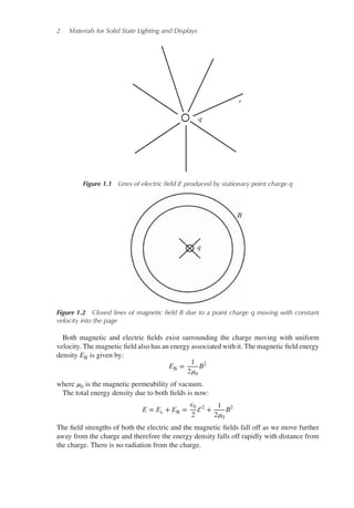
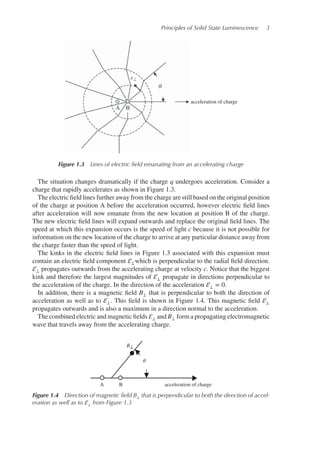
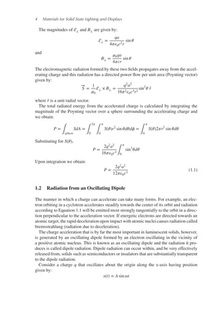
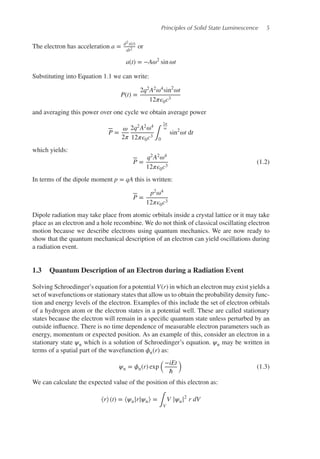
![6 Materials for Solid State Lighting and Displays
where V represents all space. Substituting the form of a stationary state we obtain:
⟨r⟩(t) =
∫V
[
𝜙(r) exp
(
−iEt
ℏ
)
𝜙(r) exp
(
iEt
ℏ
) ]
rdV =
∫V
r𝜙2
(r)dV
which is a time-independent quantity. This confirms the stationary nature of this state. A
stationary state does not radiate and there is no energy loss associated with the behavior of
an electron in such a state.
Note that electrons are not truly stationary in a quantum state from a classical viewpoint.
It is therefore the quantum state that is described as stationary and not the electron itself.
Quantum mechanics sanctions the existence of a charge that has a distributed spatial prob-
ability distribution function and yet that is in a stationary state. Classical physics fails to
describe or predict this.
Experience tells us, however, that radiation may be produced when a charge moves from
one stationary state to another and we can show that radiation is produced if an oscillating
dipole results from a charge moving from one stationary state to another. Consider a charge
q initially in normalized stationary state 𝜓n and eventually in normalized stationary state
𝜓n′ . During the transition, a superposition state is created which we shall call 𝜓s:
𝜓s = a𝜓n + b𝜓n′
where |a|2 + |b|2 = 1 to normalize the superposition state. Here, a and b are time-
dependent coefficients. Initially a = 1 and b = 0 and after the transition, a = 0 and b = 1.
If we now calculate the expectation value of the position of q for the superposition state
𝜓s we obtain:
⟨rs⟩ = ⟨a𝜓n + b𝜓n′ |r|a𝜓n + b𝜓n′ ⟩
= |a|2
⟨𝜓n|r|𝜓n⟩ + |b|2
⟨𝜓n′ |r|𝜓n′ ⟩ + a∗
b⟨𝜓n|r|𝜓n′ ⟩ + b∗
a⟨𝜓n|r|𝜓n′ ⟩
Of the four terms, the first two are stationary but the last two terms are not and therefore
⟨r⟩s(t) may be written using Equation 1.3 as:
⟨r⟩s(t) = a∗
b⟨𝜙n|r|𝜙n′ ⟩ exp
(
−i(En − En′ )t
ℏ
)
+ b∗
a⟨𝜙n|r|𝜙n′ ⟩ exp
(
i(En − En′ )t
ℏ
)
Using the Euler formula eix + e−ix = 2 cos x
we have:
⟨r⟩s(t) = a∗
b⟨𝜙n|r|𝜙n′ ⟩ exp
(
−i(En − En′ )t
ℏ
)
+ b∗
a⟨𝜙n|r|𝜙n′ ⟩ exp
(
i(En − En′ )t
ℏ
)
= 2a∗
b⟨𝜙n|r|𝜙n′ ⟩ cos
(
(En – En′ )t
ℏ
)
Defining |rnn′ | = a∗b⟨𝜙n|r|𝜙n′ ⟩ and 𝜔nn′ =
(En – En′ )
ℏ
we finally obtain:
⟨r⟩s(t) = 2|rnn′ | cos(𝜔nn′ t) (1.4)
Here, |rnn′ | is called the matrix element for the transition. It is seen that the expectation
value of the position of the electron is oscillating with frequency 𝜔nn′ =
(En – En′ )
ℏ
which is](https://image.slidesharecdn.com/3377528-250531102923-9a074377/85/Materials-For-Solid-State-Lighting-And-Displays-Kitai-Adrian-25-320.jpg)
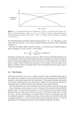
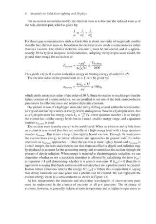
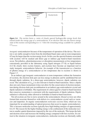
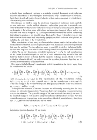
![12 Materials for Solid State Lighting and Displays
If we look for solutions for 𝜓T of the form 𝜓T = 𝜓(x1, y1, z1)𝜓(x2, y2, z2) then
Equation 1.6 becomes
−
ℏ2
2m
𝜓(x2, y2, z2)
(
𝜕2
𝜕x2
1
+
𝜕2
𝜕y2
1
+
𝜕2
𝜕z2
1
)
𝜓(x1, y1, z1)
−
ℏ2
2m
𝜓(x1, y1, z1)
(
𝜕2
𝜕x2
2
+
𝜕2
𝜕y2
2
+
𝜕2
𝜕z2
2
)
𝜓(x2, y2, z2)
+ V(x1, y1, z1)𝜓(x1, y1, z1)𝜓(x2, y2, z2)
+ V(x2, y2, z2)𝜓(x1, y1, z1)𝜓(x2, y2, z2)
= ET𝜓(x1, y1, z1)𝜓(x2, y2, z2) (1.7)
Dividing Equation 1.7 by 𝜓(x1, y1, z1)𝜓(x2, y2, z2) we obtain:
−
ℏ2
2m
1
𝜓(x1, y1, z1)
(
𝜕2
𝜕x2
1
+
𝜕2
𝜕y2
1
+
𝜕2
𝜕z2
1
)
𝜓(x1, y1, z1)
−
ℏ2
2m
1
𝜓(x2, y2, z2)
(
𝜕2
𝜕x2
2
+
𝜕2
𝜕y2
2
+
𝜕2
𝜕z2
2
)
𝜓(x2, y2, z2)
+ V(x1, y1, z1) + V(x2, y2, z2) = ET
Since the first and third terms are only a function of (x1, y1, z1) and the second and fourth
terms are only a function of (x2, y2, z2), and furthermore since the equation must be satisfied
for independent choices of (x1, y1, z1) and (x2, y2, z2) it follows that we must independently
satisfy two equations, namely
−
ℏ2
2m
1
𝜓(x1, y1, z1)
(
𝜕2
𝜕x2
1
+
𝜕2
𝜕y2
1
+
𝜕2
𝜕z2
1
)
𝜓(x1, y1, z1) + V(x1, y1, z1) = E1
and
−
ℏ2
2m
1
𝜓(x2, y2, z2)
(
𝜕2
𝜕x2
2
+
𝜕2
𝜕y2
2
+
𝜕2
𝜕z2
2
)
𝜓(x2, y2, z2) + V(x2, y2, z2) = E2
These are both identical one-electron Schrödinger equations. We have used the technique
of separation of variables.
We have considered only the spatial parts of the wavefunctions of the electrons; however,
electrons also have spin. In order to include spin the wavefunctions must also define the
spin direction of the electron.
We will write a complete wavefunction [𝜓(x1, y1, z1)𝜓(S)]a, which is the wavefunction
for one electron where 𝜓(x1, y1, z1) describes the spatial part and the spin wavefunction
𝜓(S) describes the spin part, which can be spin up or spin down. There will be four quantum
numbers associated with each wavefunction of which the first three arise from the spatial
part. A fourth quantum number, which can be +1∕2 or −1∕2 for the spin part, defines the
direction of the spin part. Rather than writing the full set of quantum numbers for each](https://image.slidesharecdn.com/3377528-250531102923-9a074377/85/Materials-For-Solid-State-Lighting-And-Displays-Kitai-Adrian-31-320.jpg)
![Principles of Solid State Luminescence 13
wavefunction we will use the subscript a to denote the set of four quantum numbers. For
the other electron the analogous wavefunction is [𝜓(x2, y2, z2)𝜓(S)]b indicating that this
electron has its own set of four quantum numbers denoted by subscript b.
Now the wavefunction of the two-electron System including spin becomes:
𝜓T1
= [𝜓(x1, y1, z1)𝜓(S)]a[𝜓(x2, y2, z2)𝜓(S)]b (1.8a)
The probability distribution function, which describes the spatial probability density func-
tion of the two-electron system, is |𝜓T|2, which can be written as:
|𝜓T1
|2
= 𝜓
∗
T1
𝜓T1
= [𝜓(x1, y1, z1)𝜓(S)]
∗
a [𝜓(x2, y2, z2)𝜓(S)]
∗
b [𝜓(x1, y1, z1)𝜓(S)]a
[𝜓(x2, y2, z2)𝜓(S)]b (1.8b)
If the electrons were distinguishable then we would need also to consider the case where
the electrons were in the opposite states, and in this case
𝜓T2
= [𝜓(x1, y1, z1)𝜓(S)]b[𝜓(x2, y2, z2)𝜓(S)]a (1.9a)
Now the probability density of the two-electron system would be:
|𝜓T2
|2
= 𝜓
∗
T2
𝜓T2
= [𝜓(x1, y1, z1)𝜓(S)]
∗
b [𝜓(x2, y2, z2)𝜓(S)]
∗
a [𝜓(x1, y1, z1)𝜓(S)]b
[𝜓(x2, y2, z2)𝜓(S)]a (1.9b)
Clearly Equation 1.9b is not the same as Equation 1.8b and when the subscripts are switched
the form of |𝜓T|2 changes. This specifically contradicts the requirement, that measurable
quantities such as the spatial distribution function of the two-electron system remain the
same regardless of the interchange of the electrons.
In order to resolve this difficulty, it is possible to write wavefunctions of the two-electron
system that are linear combinations of the two possible electron wavefunctions.
We write a symmetric wavefunction 𝜓S for the two-electron system as:
𝜓S =
1
√
2
[𝜓T1
+ 𝜓T2
] (1.10)
and an antisymmetric wavefunction 𝜓A for the two-electron system as:
𝜓A =
1
√
2
[𝜓T1
− 𝜓T2
] (1.11)
If 𝜓S is used in place of 𝜓T to calculate the probability density function |𝜓S|2, the result will
be independent of the choice of the subscripts, In addition since both 𝜓T1
and 𝜓T2
are valid
solutions to Schrödinger’s equation (Equation 1.6) and since 𝜓S is a linear combination of
these solutions it follows that 𝜓S is also a valid solution. The same argument applies to 𝜓A.
We will now examine just the spin parts of the wavefunctions for each electron. We need
to consider all possible spin wavefunctions for the two electrons. The individual electron](https://image.slidesharecdn.com/3377528-250531102923-9a074377/85/Materials-For-Solid-State-Lighting-And-Displays-Kitai-Adrian-32-320.jpg)
![14 Materials for Solid State Lighting and Displays
spin wavefunctions must be multiplied to obtain the spin part of the wavefunction for the
two-electron system as indicated in Equations 1.8 or 1.9, and we obtain four possibilities,
namely 𝜓1
2
𝜓− 1
2
or𝜓− 1
2
𝜓1
2
or𝜓1
2
𝜓1
2
or𝜓− 1
2
𝜓− 1
2
.
For the first two possibilities to satisfy the requirement that the spin part of the new two-
electron wavefunction does not depend on which electron is which, a symmetric or an anti-
symmetric spin function is required. In the symmetric case we can use a linear combination
of wavefunctions:
𝜓 =
1
√
2
(
𝜓1
2
𝜓− 1
2
+ 𝜓− 1
2
𝜓1
2
)
(1.12)
This is a symmetric spin wavefunction since changing the labels does not affect the result.
The total spin for this symmetric system turns out to be s = 1, There is also an antisym-
metric case for which
𝜓 =
1
√
2
(
𝜓1
2
𝜓− 1
2
− 𝜓− 1
2
𝜓1
2
)
(1.13)
Here, changing the sign of the labels changes the sign of the linear combination but does not
change any measurable properties and this is therefore also consistent with the requirements
for a proper description of indistinguishable particles. In this antisymmetric system the total
spin turns out to be s = 0.
The final two possibilities are symmetric cases since switching the labels makes no dif-
ference. These cases therefore do not require the use of linear combinations to be consistent
with indistinguishability and are simply
𝜓 = 𝜓1
2
𝜓1
2
(1.14)
and
𝜓 = 𝜓− 1
2
𝜓− 1
2
(1.15)
These symmetric cases both have spin s = 1.
In summary, there are four cases, three of which, given by Equations 1.12, 1.14, and
1.15, are symmetric spin states and have total spin s = 1, and one of which, given by
Equation 1.13, is antisymmetric and has total spin s = 0. Note that total spin is not always
simply the sum of the individual spins of the two electrons, but must take into account the
addition rules for quantum spin vectors. (See reference [1]) The three symmetric cases are
appropriately called triplet states and the one antisymmetric case is called a singlet state.
Table 1.1 lists the four possible states.
We must now return to the wavefunctions shown in Equations 1.10 and 1.11. The anti-
symmetric wavefunction 𝜓A may be written using Equations 1.11, 1.8a and 1.9a as:
𝜓A =
1
√
2
[𝜓T1
− 𝜓T2
]
=
1
√
2
{[𝜓(x1, y1, z1)𝜓(S)]a [𝜓(x2, y2, z2)𝜓(S)]b
−[𝜓(x1, y1, z1)𝜓(S)]b [𝜓(x2, y2, z2)𝜓(S)]a} (1.16)](https://image.slidesharecdn.com/3377528-250531102923-9a074377/85/Materials-For-Solid-State-Lighting-And-Displays-Kitai-Adrian-33-320.jpg)
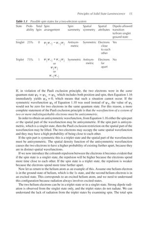
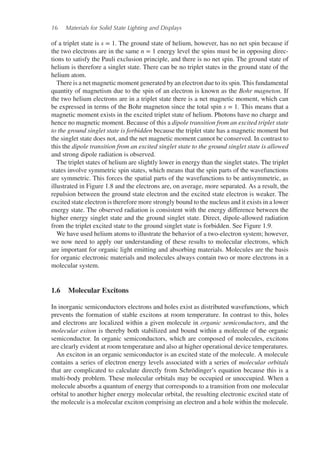
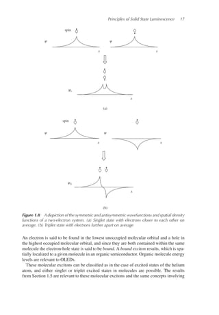
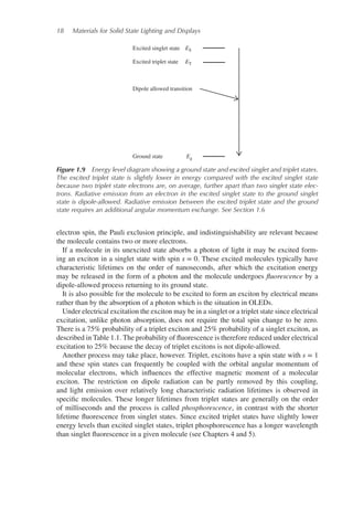
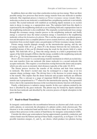
![22 Materials for Solid State Lighting and Displays
Recognizing that the density of states function must be zero for E < Eg we obtain:
Djoint(E) =
1
2
𝜋
(
2𝜇
𝜋2ℏ2
)3
2
(E − Eg)
1
2 (1.18)
This is known as the joint density of states function valid for E ≥ Eg.
To determine the probability of occupancy of states in the bands, we use Fermi–Dirac
statistics. The Boltzmann approximation for the probability of occupancy of carriers in a
conduction band is:
F(E) ≅ exp
[
−
(Ee − Ef)
kT
]
and for a valence band the probability of a hole is given by:
1 − F(E) ≅ exp
[
(Eh − Ef)
kT
]
Since a transition requires both an electron in the conduction band and a hole in the valence
band, the probability of a transition will be proportional to:
F(E)[1 − F(E)] = exp
(
−
(Ee − Eh)
kT
)
= exp
(
−
E
kT
)
(1.19)
Including the density of states function, we conclude that the probability p(E) of an
electron–hole pair recombination applicable to an LED is proportional to the product of
the joint density of states function and the function F(E)[1 − F(E)], which yields:
p(E) ∝ D(E − Eg)F(E)[1 − F(E)] (1.20)
Now using Equations 1.18, 1.19, and 1.20, we obtain the photon emission rate R(E) as:
R(E) ∝ (E − Eg)1∕2
exp
(
−
E
kT
)
(1.21)
The result is shown graphically in Figure 1.11.
If we differentiate Equation 1.21 with respect to E and set dR(E)
dE
= 0 the maximum is
found to occur at E = Eg + kT
2
. From this, we can evaluate the full width at half maximum
to be 1.8kT.
If we were interested in optical absorption instead of emission for a direct gap semicon-
ductor, the absorption constant 𝛼 can be evaluated using Equation 1.18 and we obtain:
𝛼(hv) ∝ (hv − Eg)
1
2 (1.22)
We consider the valence band to be fully occupied by electrons and the conduction band
to be empty. In this case the absorption rate depends on the joint density of states function
only and is independent of Fermi–Dirac statistics. The absorption edge for a direct gap
semiconductor is illustrated in Figure 1.12.
This absorption edge is only valid for direct gap semiconductors, and only when parabolic
band-shapes are valid. If hv ≫ Eg this will not be the case and measured absorption coef-
ficients will differ from this theory.
In an indirect gap semiconductor, the absorption 𝛼 increases more gradually with photon
energy hv until a direct gap transition can occur.](https://image.slidesharecdn.com/3377528-250531102923-9a074377/85/Materials-For-Solid-State-Lighting-And-Displays-Kitai-Adrian-41-320.jpg)
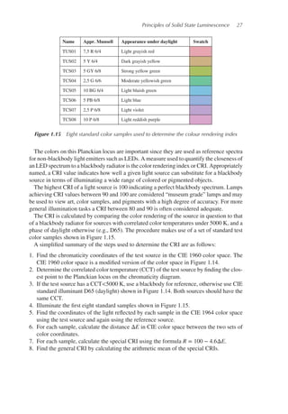
![28 Materials for Solid State Lighting and Displays
1.9 The Light Emitting Diode
The most important means of achieving electron–hole pair recombination producing radi-
ation is via a p-n junction diode. In this section the key concepts underlying p-n junction
operation are summarized and for reference, detailed quantitative treatments are avail-
able [1–4].
First we will consider the case of a diode in equilibrium without a current or voltage
applied to it. The band model of a p-n junction is shown in Figure 1.16. A built-in electric
field exits at the diode junction and this field gives rise to a potential difference V0 across
the junction.
In the conduction band, equal and opposite electron currents flow comprising an electron
drift current due to the built-in electric field and an opposing electron diffusion current
due to the large concentration gradient of electrons across the junction. Similarly, in the
valence band, equal and opposite hole currents flow comprising a hole drift current due to
the built-in electric field and an opposing hole diffusion current due to the large concentra-
tion gradient of holes across the junction. The net diode current is zero.
If a potential V is now applied to the diode the built-in electric field is modified. A positive
value of V which is described as a forward bias decreases the built-in electric field as shown
in Figure 1.17. This results in an increase of diffusion current relative to drift current and
a rapid and approximately exponential increase in net diode current occurs as V increases.
If the applied voltage is negative, then the built-in electric field increases as shown in
Figure 1.18. This results in a larger potential barrier that favors drift current but not diffusion
current. A net drift current flows but the drift current is small since it is only supplied by
the small minority carrier concentration of electrons in the p-side and the small minority
concentration of holes in the n-side of the diode. This drift current, being supply limited,
saturates with increasingly negative applied voltage.
p-side
Ec
In diffusion
Ip diffusion
In drift
Ip drift
Ɛ
Ef
Ev
n-side
qV0
Figure 1.16 Band diagram of a p-n junction in equilibrium showing hole and electron cur-
rents. The net current is zero. V0 is the built-in potential of the junction](https://image.slidesharecdn.com/3377528-250531102923-9a074377/85/Materials-For-Solid-State-Lighting-And-Displays-Kitai-Adrian-47-320.jpg)
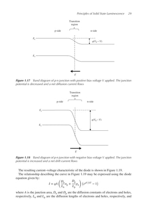
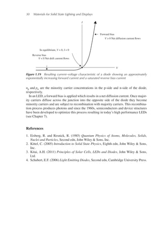
![2
Quantum Dots for Displays and Solid
State Lighting
Jesse R. Manders1, Debasis Bera2,3, Lei Qian2,3 and Paul H. Holloway2,3
1Nanosys, Inc., Milpitas, CA, USA
2NanoPhotonica, Inc., Alachua, FL, USA
3Department of Materials Science and Engineering, University of Florida, Gainesville,
FL, USA
2.1 Introduction
The word “phosphor” comes from the Greek language and means “light bearer” to describe
light emitting materials or luminescent material; barium sulfide is one of the earlier known
naturally occurring phosphors [1]. A phosphor is luminescent, that is emits energy from
an excited electron as light, where the excitation of the electron is caused by absorption of
energy from an external source such as another electron, a photon, an electric field, or heat.
An excited electron occupies a quantum state whose energy is above the minimum energy
ground state. In semiconductors and insulators, the electronic ground state is commonly
referred to as electrons in the valence band which is completely filled with electrons. The
excited quantum state often lies in the conduction band which is empty and is separated
from the valence band by an energy gap called the band gap, ΔEg in Figure 2.1. Therefore,
unlike metallic materials, small continuous changes in electron energy within the band are
not possible. Instead a minimum energy equal to the band gap is necessary to excite an
electron in a semiconductor or insulator, and the energy released by de-excitation is often
nearly equal to the band gap. For a semiconductor, the band gap energy is sufficiently large
that at room temperature, very few electrons are promoted from the valence band to the
conduction band, a process which leaves holes in the valence band. Figure 2.1(a) shows
an energy band diagram (plot of allowed quantum state energy versus wave vector mag-
nitude k) for a direct band gap semiconductor. In the direct band gap semiconductors, the
Materials for Solid State Lighting and Displays, First Edition. Edited by Adrian Kitai.
© 2017 John Wiley & Sons Ltd. Published 2017 by John Wiley & Sons Ltd.](https://image.slidesharecdn.com/3377528-250531102923-9a074377/85/Materials-For-Solid-State-Lighting-And-Displays-Kitai-Adrian-50-320.jpg)
![32 Materials for Solid State Lighting and Displays
Energy
0
EC
2me
=
EV
2mh
ħ2
k2
ħ2k2
=
ΔEg
Valence
Band
Valence
Band
Conduction
Band
k
Wave vector
HOMO
LUMO
0 k
Wave vector
(a) (b)
Conduction
Band
Virtual State
ΔEg
Figure 2.1 Schematic band-energy diagrams for (a) direct band gap and (b) indirect band
gap semiconductors
positions of the highest energy state of the valence band and the lowest energy state of the
largely unoccupied conduction band are at the same k resulting in a high probability of
emitting light. The case of an indirect band gap semiconductor is shown in Figure 2.1(b)
and has the valence band maximum and conduction band minimum at different values
of k. Therefore, electrons need to undergo a change of k-value followed by a change in
energy. That is, the transition requires a change of both in energy and momentum. In other
words, an indirect transition requires energy excitation of an electron simultaneous with
an electron–phonon interaction to give the required momentum change. Therefore, the
absorption and recombination efficiency of direct band gap materials is about four orders of
magnitude larger than that of indirect material. Zinc sulfoselenide (ZnS1−xSex) and gallium
phosphide (GaP) are examples of direct and indirect band gap compound semiconductors,
respectively.
As discussed above, luminescence from phosphors can be observed by exciting the elec-
trons to higher energy states, for example into the conduction band. There are several
approaches to provide this excitation, such as photoluminescence (PL), electrolumines-
cence (EL), cathodoluminescence (CL), mechanoluminescence, chemiluminescence, and
thermoluminescence [1]. In this chapter, only PL, EL, and CL (Figure 2.2) will be dis-
cussed, with most emphasis being on PL and EL.
When an insulator or semiconductor absorbs electromagnetic radiation (i.e., a photon)
an electron may be excited to a higher energy quantum state. If the excited electron returns
(relaxes) to a lower energy quantum state by radiating a photon, the process is called PL.
Some of the quantum state relaxation transitions are not allowed based on the spin and
Laporte selection rules [2]. The PL intensity depends on the measurement temperature and
the energy of the exciting light (known as photoluminescence excitation or PLE spectrum).](https://image.slidesharecdn.com/3377528-250531102923-9a074377/85/Materials-For-Solid-State-Lighting-And-Displays-Kitai-Adrian-51-320.jpg)
![Quantum Dots for Displays and Solid State Lighting 33
Secondary electron
X-rays
High-energy
electron
High-energy
photon
absorption
Low-energy
photon
emission
electrode
electrode
Emission
Auger electron
UV, Visible,
IR emission
(a)
(b)
(c)
Back-scattered
electron
Figure 2.2 Schematic illustrations of (a) photoluminescence, (b) electroluminescence, and
(c) cathodoluminescence
In general, peaks in the PLE spectrum are higher in energy than those in the PL spectrum.
Figure 2.2(a) schematically illustrates the excitation and emission processes of PL.
When a material emits electromagnetic radiation as a result of the application of an
electric field, the process is called EL. The photon emission results from radiative recom-
bination of electrons and holes created in - or injected into - the phosphor by the voltage
between the two electrodes, as shown in Figure 2.2(b). One of the electrodes is transparent
to the wavelength of the light emitted by the device. The first report of an EL device was in
1907 [3], when Henry Joseph Round observed that light was emitted from silicon carbide
under the application of a high voltage. As discussed below, there is significant interest
in inorganic nanophosphors combined with conducting organic materials to produce EL
devices because of their potentially high efficiencies. Other advantages for EL devices in
comparison with conventional lighting systems also include a large size range, flexible
substrates and shapes, high brightness, long device lifetimes, lower operating tempera-
tures, non-directionality and antiglare lighting. Depending on the applied bias, a thin-film
electroluminescence (TFEL) device can be categorized as either a DC or AC (ACTFEL)
device.
Cathodoluminescence is emission of light from a material that is excited by energetic
electrons. The exciting primary electrons can be focused into a beam and scanned across
the surface (as in a scanning electron microscope) resulting in high spatial resolution CL.
The CL process is shown schematically in Figure 2.2(c), along with other phenomena that
result from primary electron–material interactions, for example X-ray and various electron
emissions.](https://image.slidesharecdn.com/3377528-250531102923-9a074377/85/Materials-For-Solid-State-Lighting-And-Displays-Kitai-Adrian-52-320.jpg)
![34 Materials for Solid State Lighting and Displays
2.2 Nanostructured Materials
Nanostructured materials, by definition, can exist as individual particles or clusters of
nanoparticles with various shapes and sizes [4, 5] . Research has shown that nanostructured
materials generally exhibit geometries that reflect the atomistic bonding analogous to the
bulk structure. The nanomaterials are of interest because they can bridge the gap between
the bulk and molecular levels and lead to entirely new avenues for applications. Nano-
structured materials have a very high surface-to-volume ratio compared with their bulk
counterparts. Therefore, a large fraction of atoms is present on the surface which makes
them possess different thermodynamic properties. During the last two decades, a great deal
of attention has been focused on the optoelectronic properties of nanostructured semicon-
ductors with an emphasis on fabrication of the smallest possible particles. The research has
revealed that many fundamental properties are size dependent in the nanometer range. For
example, the density of quantum states (DOS) versus energy for periodic materials with
three, two or one dimensions is shown in Figure 2.3. (See reference [6] for detailed expla-
nations.) If the extent of the material is on the order of 1–10 nm in all three directions,
the material is said to be quantum dots (QDs). A QD is zero dimensional relative to the
bulk, and the DOS depends upon whether or not the QDs have aggregated, as shown in
Figure 2.3. The DOS for a molecule and an atom are also shown in Figure 2.3 (see refer-
ence [6]). The density of electrons in a three-dimensional bulk crystal is so large that the
energy of the quantum states becomes nearly continuous as shown in Figure 2.3. However,
the limited number of electrons results in discrete quantized energies in the DOS for two-,
one- and zero-dimensional structures (Figure 2.3). The presence of one electronic charge
HOM
LUM
MO theory
A
A
A
Atom
Molecule
QDs
Bulk Material
Density of States (DOS)
Energy
N(E)
Dimension
zero
zero
zero
Three, two
or one
Diameter
1.2 A
1-3 nm
1-20 nm
> 20 nm
3D 2D 1D
Series of QDs Few QDs One QD
Few molecules Single molecule
Figure 2.3 Schematic illustration of the changes of the density of quantum states with
changes in the number of atoms in materials (see text for a detailed explanation)](https://image.slidesharecdn.com/3377528-250531102923-9a074377/85/Materials-For-Solid-State-Lighting-And-Displays-Kitai-Adrian-53-320.jpg)
![Quantum Dots for Displays and Solid State Lighting 35
in the QDs repels the addition of another charge and leads to a staircase-like I–V curve
and DOS. The step size of the staircase is proportional to the reciprocal of the radius of
the QDs. The boundaries as to when a material has the properties of bulk, QDs or atoms
are dependent upon the composition and crystal structure of the compound or elemental
solid. When a solid exhibits a distinct variation of optical and electronic properties with
a variation of size, it can be called a nanostructure, and is categorized as (1) two dimen-
sional, for example thin films or quantum wells, (2) one dimensional, for example quantum
wires, or (3) zero dimensional, for example QDs. Although each of these categories shows
interesting optical properties, our discussion will be focused on QDs. An enormous range
of fundamental properties can be realized by changing the size at a constant composition
or by changing the composition at constant size. In the following sections, we will discuss
the history, structure and properties relationships, and the optical properties of QDs.
2.3 Quantum Dots
Nanostructured semiconductors or insulators have dimensions and numbers of atoms
between the atomic-molecular level and bulk material with a band gap that depends in
a complicated fashion upon a number of factors, including the bond type and strength
with the nearest neighbors. For isolated atoms, there is no nearest-neighbor interaction.
Therefore, sharp and narrow luminescent emission peaks are observed. A molecule
consists of only a few atoms and therefore exhibits emission similar to that of an atom. A
nanoparticle, however, is composed of approximately 100–10 000 atoms, and has optical
properties distinct from its bulk counterpart. Nanoparticles with dimensions in the range
of 1–20 nm are called QDs. Zero-dimensional QDs are often described as artificial atoms
due to their 𝛿-function-like DOS which can lead to narrow optical line spectra.
A significant amount of current research is aimed at using the unique optical properties
of QDs in devices, such as light emitting diodes (LEDs), solar cells and biological
markers. QDs are of interest in biology for several reasons including (1) higher extinction
coefficients, (2) higher quantum yields, (3) less photobleaching, (4) absorbance and
emissions can be tuned with size, (5) generally broad excitation window but narrow
emission peaks, (6) multiple QDs can be used in the same assay with minimal interference
with each other, (7) toxicity may be less than conventional organic dyes, and (8) the QDs
may be functionalized with different bio-active agents [7–9]. The inorganic QDs are more
photostable under ultraviolet excitation than are organic molecules, and their fluorescence
is more saturated. The ability to synthesize QDs with narrow size distributions with high
quantum yields [10, 11] has made QDs an attractive alternative to organic molecules in
hybrid LEDs and solar cells.
QDs can be broadly categorized into either elemental or compound systems. In this
chapter, we will emphasize compound semiconductor based nanostructured materials.
Compound materials can be categorized according to the columns in the periodic table, for
example IB–VIIB (CuCl, CuBr, CuI, AgBr, etc.), IIB–IVB (ZnO, ZnS, ZnSe, ZnTe, CdO,
CdS, CdSe, CdTe, etc.), IIIB–VB (GaN, GaP, GaAs, InN, InP, InSb, etc.), and IVB–VIB
(PbS, PbSe, PbTe, etc.). Our discussion will be confined mainly to IIB–VIB, IIIB–VB and
IVB–VIB QDs based phosphors, where frequently the B designations are dropped, that is
the compounds are designated as II–VI or III–V.](https://image.slidesharecdn.com/3377528-250531102923-9a074377/85/Materials-For-Solid-State-Lighting-And-Displays-Kitai-Adrian-54-320.jpg)


![[S.L._Kakani]_Material_Science_(New_Age_Pub.,_2006(BookSee.org).pdf](https://cdn.slidesharecdn.com/ss_thumbnails/s-230301071329-4f25d7e9-thumbnail.jpg?width=640&height=640&fit=bounds)


