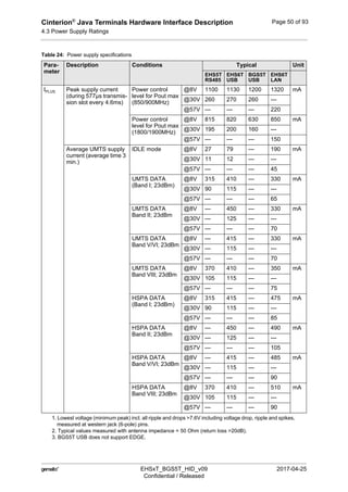
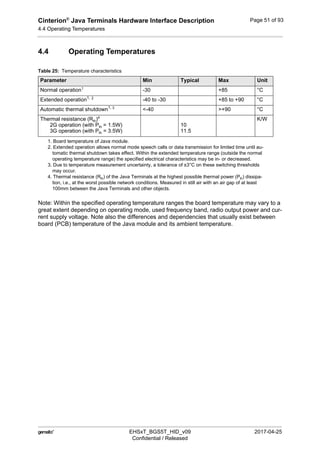
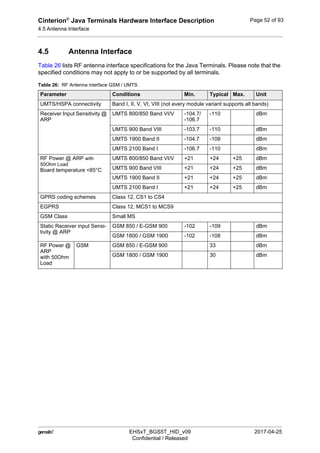
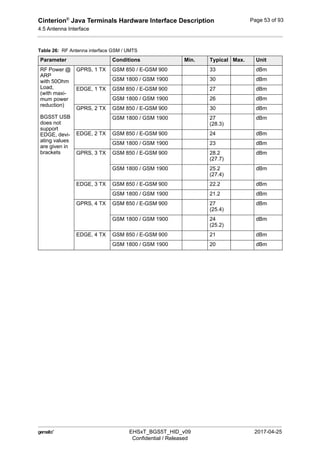
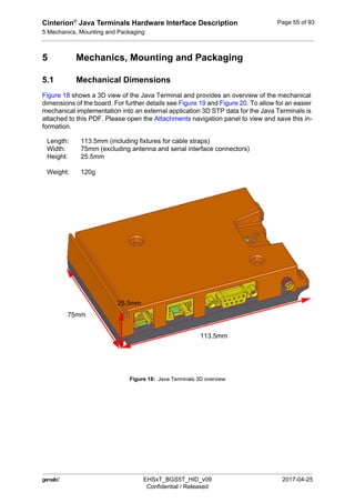
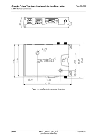
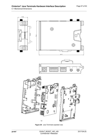
This document provides information on the hardware interfaces, electrical specifications, mechanical dimensions, and regulatory compliance of Gemalto's Cinterion Java Terminals, including the EHS5T-RS485, EHS6T USB, EHS6T LAN, and BGS5T USB models. It covers topics such as the RS-232, USB, GPIO, Ethernet, power supply, SIM, antenna, and status LED interfaces. Specifications for voltage, temperature range, packaging, and approvals are also included along with diagrams of the terminal circuitry, connectors, and dimensions. The document history notes recent additions of the EHS5T-RS485 model and updated information on regulatory compliance.
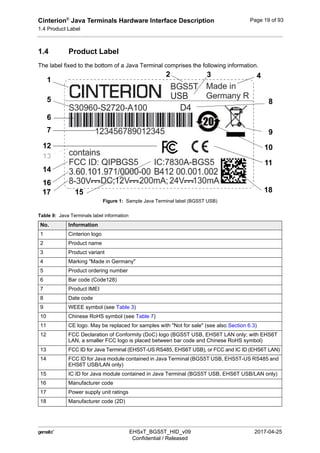
![Cinterion®
Java Terminals Hardware Interface Description
1.1 Related Documents
19
EHSxT_BGS5T_HID_v09 2017-04-25
Confidential / Released
Page 12 of 93
1.1 Related Documents
[1] AT Command Set for your Java Terminal product
[2] Release Notes for your Java Terminal product
To visit the Gemalto M2M GmbH Website please use the following link:
http://m2m.gemalto.com
1.2 Terms and Abbreviations
Table 2: Terms and abbreviations
Abbreviation Description
ARP Antenna Reference Point
ATC AT Command
BTS Base Transceiver Station
CB Cell Broadcast
CODEC Coder-Decoder
DAI Digital Audio Interface
DCE Data Circuit terminating Equipment
DSR Data Set Ready
DTR Data Terminal Ready
EFR Enhanced Full Rate
EGSM Enhanced GSM
EMC Electromagnetic Compatibility
ESD Electrostatic Discharge
ETS European Telecommunication Standard
FDMA Frequency Division Multiple Access
G.C.F. GSM Conformity Forum
GSM Global Standard for Mobile Communication
HW Hardware
I2
C Inter Integrated Circuit
IC Integrated Circuit
IF Intermediate Frequency
IMEI International Mobile Equipment Identifier
I/O Input/ Output
IGT Ignition
ISO International Standards Organization
ITU International Telecommunications Union](https://image.slidesharecdn.com/m2mehs6thardware-190619161040/85/M2-m-ehs6t_hardware-12-320.jpg)
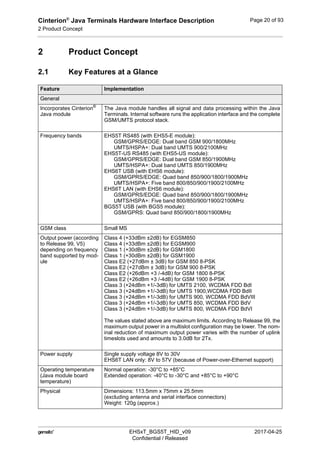
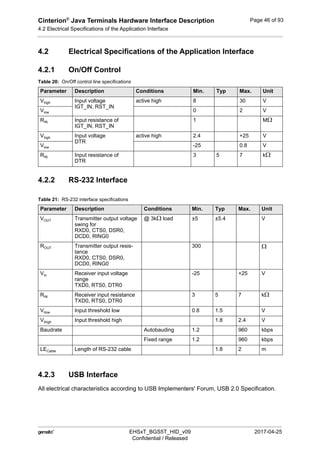
![Cinterion®
Java Terminals Hardware Interface Description
3.7 GPIO Interface
44
EHSxT_BGS5T_HID_v09 2017-04-25
Confidential / Released
Page 31 of 93
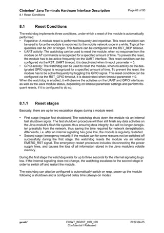
EHS5T‘s RS-485 interface is based on the TIA/EIA-485 standard defining electrical character-
istics of drivers and receivers for use in balanced multidrop communication systems. RS-485
is used in a lot of different fieldbus systems like Profibus, Interbus, Modbus and P-net.
RS-485 uses a shielded twisted pair cable where the inner pairs are used for balanced com-
munication. The two conductors in each pair are called A and B. RS-485 is usually half-duplex.
Data transmission speed depends on the length of the RS-485 bus cable and may be up to
115kbps.
Note: If employing EHS5T‘s RS-485 interface be sure not to switch off the EHS5 module, e.g.,
by calling AT^SMSO, to put the module into Power Down mode. This completely occupies and
therefore blocks the RS-485 bus, and may thus lead to a higher current consumption.
Also, be sure not to activate SLEEP mode, e.g., by setting AT^SPOW with <mode>=2, for the
EHS5 module, as the module may no longer be able to wake up from SLEEP mode, and will
then have to be reset.
3.7.1 Serial Interface ASC1
With EHS5T and EHS6T Java Terminals two respectively four pins at the GPIO connector can
be configured as ASC1 interface signals to provide a 2- or 4-wire serial modem interface ASC1.
For electrical characteristics please refer to Table 22.
The following pins at the GPIO connector can be configured as ASC1 interface signals: RXD1,
TXD1, RTS1 and CTS1 (see also Table 13). The configuration is done by AT command
AT^SCFG - see [1]. It is non-volatile and becomes active after a Java Terminal restart.
Java Terminals are designed for use as a DCE. Based on the conventions for DCE-DTE con-
nections they communicate with the customer application (DTE) using the following signals:
• Port TXD @ application sends data to Java Terminal’s TXD1 signal line
• Port RXD @ application receives data from the Java Terminal’s RXD1 signal line
Hardware handshake using the RTS1 and CTS1 signals is only supported for EHS6T.](https://image.slidesharecdn.com/m2mehs6thardware-190619161040/85/M2-m-ehs6t_hardware-31-320.jpg)
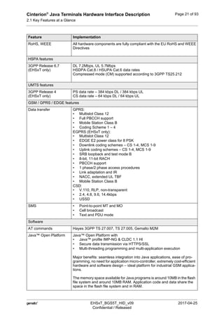
![Cinterion®
Java Terminals Hardware Interface Description
3.7 GPIO Interface
44
EHSxT_BGS5T_HID_v09 2017-04-25
Confidential / Released
Page 32 of 93
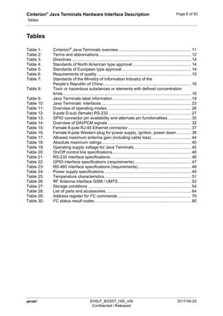
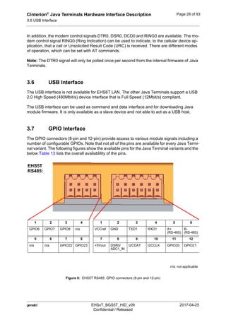
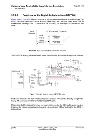
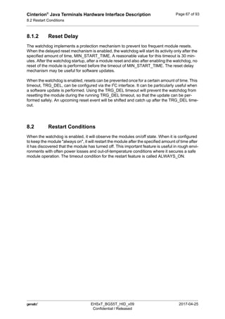
3.7.2 Digital Audio Interface
Four pins at the Java Terminals‘ GPIO connector can be configured as digital audio interface
(DAI). The DAI can be used to connect audio devices capable of pulse code modulation (PCM).
The PCM functionality allows for the use of an external codec like the W681360.
The DAI interface supports a 256kHz, long frame synchronization master mode with the follow-
ing features:
• 16 Bit linear
• 8kHz sample rate / 125µs frame duration
• The most significant bit MSB is transferred first
• Data write at rising edge / data read at falling edge
• Common frame sync signal for transmit and receive
The following pins at the GPIO connector can be configured as DAI/PCM interface signals:
TXDDAI, RXDDAI, TFSDAI and SCLK (see also Table 13). The configuration is done by
AT^SCFG command - see [1]. It is non-volatile and becomes active after a module restart. DAI/
PCM and GPIO functionalities for these lines are mutually exclusive. Table 14 describes the
available DAI/PCM lines at the digital audio interface1
. For electrical details see Table 22.
Figure 9 shows the PCM timing for the master mode available with Java Terminals.
Figure 9: Long frame PCM timing, 256kHz
Section 3.7.2.1 gives an example of how the DAI can be employed.
1. Note: For the DAI interface to operate, the directions of the Java Terminals‘ GPIO level shifters must
be set according to the defined directions of the DAI signals. See Section 8.3.1.11 and Section 8.5 for
more information on how to change level shifter directions.
Table 14: Overview of DAI/PCM signals
Signal name Input/Output Description
TXDDAI (GPIO20) O PCM data from Java Terminals to external codec.
RXDDAI (GPIO21) I PCM data from external codec to Java Terminals.
TFSDAI (GPIO22) O Frame synchronization signal to external codec:
Long frame (8kHz)
SCLK (GPIO23) O Bit clock to external codec: 256kHz
SCLK
TXDDAI
RXDDAI
TFSDAI
MSB
MSB
LSB
LSB
14 13
14 13
1
1
12
12
2
2
MSB
MSB
125µs
11](https://image.slidesharecdn.com/m2mehs6thardware-190619161040/85/M2-m-ehs6t_hardware-32-320.jpg)
![Cinterion®
Java Terminals Hardware Interface Description
3.7 GPIO Interface
44
EHSxT_BGS5T_HID_v09 2017-04-25
Confidential / Released
Page 34 of 93
3.7.3 I2
C Interface
Two lines of the Java Terminals‘ GPIO connector are I2
C lines. I2
C is a serial, 8-bit oriented
data transfer bus for bit rates up to 400kbps in Fast mode. It consists of two lines, the serial
data line I2CDAT and the serial clock line I2CCLK. The Java Terminals‘ internal Java module
act as a single master device, e.g. the clock I2CCLK is driven by the Java module. I2CDAT is
a bi-directional line. Each device connected to the bus is software addressable by a unique 7-
bit address, and simple master/slave relationships exist at all times. The Java module operates
as master-transmitter or as master-receiver. An external application transmits or receives data
only on request of the module.
To configure and activate the I2C bus use the AT^SSPI command. Detailed information on the
AT^SSPI command as well explanations on the protocol and syntax required for data transmis-
sion can be found in [1].
With the external application, I2CDAT and I2CCLK lines need to be connected to a positive
supply voltage via a pull-up resistor. For electrical characteristics please refer to Table 22.
Note: Good care should be taken when connecting the I2C lines to the external application: The
wires of I2CCLK and I2CDAT should be equal in length and as short as possible.](https://image.slidesharecdn.com/m2mehs6thardware-190619161040/85/M2-m-ehs6t_hardware-34-320.jpg)
![Cinterion®
Java Terminals Hardware Interface Description
3.7 GPIO Interface
44
EHSxT_BGS5T_HID_v09 2017-04-25
Confidential / Released
Page 35 of 93
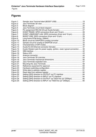
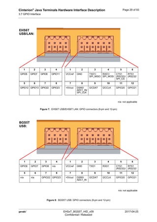
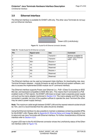
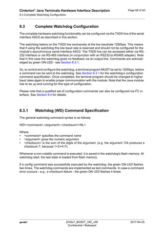
3.7.4 SPI Interface
For EHS6T Java Terminals four GPIO interface pins can be configured as Serial Peripheral In-
terface (SPI). The SPI is a synchronous serial interface for control and data transfer between
Java Terminals and the external application. Only one application can be connected to the SPI
and the interface supports only master mode. The transmission rates are up to 6.5Mbit/s. The
SPI interface comprises the two data lines MOSI and MISO, the clock line SPI_CLK a well as
the chip select line SPI_CS.
The following pins at the GPIO connector can be configured as SPI interface signals: SPI_CLK,
SPI_MOSI, SPI_MISO and SPI_CS (see also Table 13). The configuration is done by AT com-
mand (see [1]). It is non-volatile and becomes active after a module restart. For electrical char-
acteristics please refer to Table 22.
To configure and activate the SPI interface use the AT^SSPI command. Detailed information
on the AT^SSPI command as well explanations on the SPI modes required for data transmis-
sion can be found in [1]. SPI, ADC1_IN and DSR0 functionalities are mutually exclusive.
In general, SPI supports four operation modes. The modes are different in clock phase and
clock polarity. The module’s SPI mode can be configured by using the AT command AT^SSPI.
Make sure the module and the connected slave device works with the same SPI mode.
Figure 12 shows the characteristics of the four SPI modes. The SPI modes 0 and 3 are the most
common used modes.
Figure 12: Characteristics of SPI modes
SPI MODE 0 SPI MODE 1
SPI MODE 2 SPI MODE 3
Clock phase
Clockpolarity
SPI_CS
MOSI
SPI_CLK
MISO
SPI_CS
MOSI
SPI_CLK
MISO
SPI_CS
MOSI
SPI_CLK
MISO
SPI_CS
MOSI
SPI_CLK
MISO
Sample Sample
Sample Sample](https://image.slidesharecdn.com/m2mehs6thardware-190619161040/85/M2-m-ehs6t_hardware-35-320.jpg)
![Cinterion®
Java Terminals Hardware Interface Description
3.7 GPIO Interface
44
EHSxT_BGS5T_HID_v09 2017-04-25
Confidential / Released
Page 36 of 93
3.7.5 PWM Interface
The GPIO6 and GPIO7 pins at the GPIO connector can be configured as Pulse Width Modu-
lation signals PWM1 and PWM2 by AT^SCFG command - see [1]. The PWM interface lines
are output lines and can be used, for example, to connect buzzers. The PWM1 line is shared
with GPIO7 and the PWM2 line is shared with GPIO6 (see also Table 13). GPIO and PWM
functionalities are mutually exclusive1
.
3.7.6 Pulse Counter
The GPIO8 pin at the GPIO connector can be configured as pulse counter line COUNTER by
AT^SCFG command - see [1]. The pulse counter interface is an input line and can be used, for
example, as a clock (see also Table 13). GPIO and COUNTER functionalities are mutually ex-
clusive1
.
3.7.7 Analog-to-Digital Converter (ADC)
ADC1_IN can be used for general purpose voltage measurements. For electrical characteris-
tics see Section 4.2.4. ADC1_IN is configured and read by the AT^SRADC command - see [1].
ADC1_IN, DSR0 and SPI functionalities are mutually exclusive.
3.7.8 DSR0 signal
The DSR0 line available at the RS-232 interface is also routed to the GPIO connector and avail-
able as a separate pin. For electrical characteristics see Section 4.2.4. DSR0 can be configured
by AT^SCFG command - see [1]. DSR0, ADC1_IN and SPI functionalities are mutually exclu-
sive.
1. Note: For the PWM interface and pulse counter to operate, the directions of the Java Terminals‘ GPIO
level shifters must be set according to the defined directions of the PWM and COUNTER signals. See
Section 8.3.1.11 and Section 8.5 for more information on how to change level shifter directions.](https://image.slidesharecdn.com/m2mehs6thardware-190619161040/85/M2-m-ehs6t_hardware-36-320.jpg)
![Cinterion®
Java Terminals Hardware Interface Description
3.10 Power Up/Power Down Scenarios
44
EHSxT_BGS5T_HID_v09 2017-04-25
Confidential / Released
Page 39 of 93
Mains adapter: If it fits into the design of your application we recommend the plug-in supply unit
used with the type approved Gemalto M2M reference setup. Ordering information can be found
in Chapter 7. This 12V mains adapter comes with a 6-pole Western plug and provides an inter-
nal connection between IGT_IN pin and PLUS pin. If there is such an “auto ignition” connection
between PLUS and IGT_IN, the module will restart automatically after a normal shutdown. Note
that if employing PoE for EHS6T LAN, the module will also restart automatically after a normal
shutdown.
3.10 Power Up/Power Down Scenarios
In general, be sure not to turn on the Java Terminals while it is beyond the safety limits of volt-
age and temperature stated in Section 4.1. Java Terminals immediately switch off after having
started and detected these inappropriate conditions. In extreme cases this can cause perma-
nent damage to the Java Terminals.
3.10.1 Turn Java Terminals on
There are various possibilities to turn on Java Terminals and start into normal mode, depending
on connecting and/or operating states.
If powered off (i.e., if Java Terminals‘ power supply is disconnected):
• Java Terminals can simply be started up by plugging an appropriate power supply unit
between PLUS and GND of the 6-pole Western jack. If using the PoE feature, EHS6T LAN
can also be started up by connecting simply the Ethernet interface
If switched off (i.e., while in Power Down mode):
• Java Terminals can be started up by activating the IGT_IN signal (pin 4).
• Java Terminals can be started up by activating the RS-232 DTR line (as long as RST_IN
signal (pin 3) is not active (voltage <2V)
• Java Terminals can be started up by configuring the watchdog appropriately. For details
see Chapter 8.
Note: With an “auto-ignition“ connection between IGT_IN and PLUS, or if employing PoE (see
Section 3.9), Java Terminals will automatically restart into normal mode after switch off (see
Section 3.10.3). The start up variant from Power Down mode is therefore only applicable if
there is no such “auto-ignition“ connection at the power supply unit.
3.10.2 Reset/Restart Java Terminals
There are various possibilities to reset/restart Java Terminals:
• Java Terminals can be reset/restarted by entering the command AT+CFUN=x,1. For details
on AT+CFUN please see [1].
• Java Terminals can be reset/restarted by configuring the watchdog appropriately. For
details see Chapter 8.
• Java Terminals can be reset/restarted by configuring a wake-up alarm (see Section 3.13)
before using AT^SMSO to turn them off and send them into Power Down mode.](https://image.slidesharecdn.com/m2mehs6thardware-190619161040/85/M2-m-ehs6t_hardware-39-320.jpg)
![Cinterion®
Java Terminals Hardware Interface Description
3.11 Automatic thermal shutdown
44
EHSxT_BGS5T_HID_v09 2017-04-25
Confidential / Released
Page 41 of 93
3.11 Automatic thermal shutdown
An on-board NTC measures the temperature of the built-in Java module. If over- or undertem-
perature is detected on the module the Java Terminals automatically shut down to avoid ther-
mal damage to the system. Table 25 specifies the ambient temperature threshold for the Java
Terminals.
The automatic shutdown procedure is equivalent to the power-down initiated with the AT^SM-
SO command, i.e. Java Terminals log off from the network and the software enters a secure
state avoiding loss of data.
Alert messages transmitted before the Java Terminals switch off are implemented as Unsolic-
ited Result codes (URCs). For details see the description of AT^SCTM command provided in
[1].
The watchdog can be configured to restart the Java Terminals after a defined period of time.
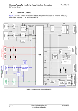
3.12 Hardware Watchdog
The Java Terminals feature a programmable hardware watchdog that permanently monitors
the terminals hardware and can be configured to react to various hardware states. The watch-
dog may for example be configured to periodically restart the terminal, independent of its cur-
rent operating state. Figure 4 shows how the watchdog is integrated into the Java Terminals.
Please refer to Chapter 8 for details on how to control and configure the hardware watchdog.
3.13 RTC
The internal Real Time Clock (RTC) of the Java Terminals retains the time and date and han-
dles the alarm function. The AT+CCLK command serves to set the time and date, and AT+CA-
LA specifies a reminder message or sets an alarm for the .Java Terminals to wake up. See [1]
for details.
A dedicated voltage regulator backs up the RTC even in Power Down mode and enables Java
Terminals to keep track of time and date.
However, please note that the Alarm function described in [1], Section AT+CALA, will only work
if there is no “auto ignition“ connection active between IGT_IN pin and PLUS pin at the power
supply unit that will automatically trigger a restart (see Section 3.9). Otherwise, the AT+CALA
command can only be used to set a reminder message, but not to configure the Java Terminals
to wake up from Power Down mode.](https://image.slidesharecdn.com/m2mehs6thardware-190619161040/85/M2-m-ehs6t_hardware-41-320.jpg)
![Cinterion®
Java Terminals Hardware Interface Description
3.15 Status LEDs
44
EHSxT_BGS5T_HID_v09 2017-04-25
Confidential / Released
Page 43 of 93
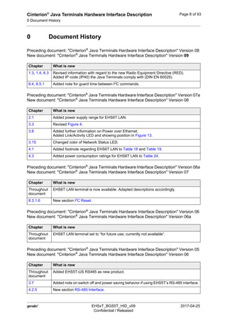
3.15 Status LEDs
Java Terminals have two LEDs indicating its operating states through the semitransparent cas-
ing:
• A green LED indicates whether the Java Terminals are ready to operate and reports certain
watchdog operations.
• A orange LED indicates the network registration state of the Java Terminals.
Figure 16: Status LED
The orange LED can be configured by using the AT^SLED command to either light permanent-
ly or to flash. For details on the AT command please refer to [1].
Green LED
(Power on/off)
Orange LED
(Network status)](https://image.slidesharecdn.com/m2mehs6thardware-190619161040/85/M2-m-ehs6t_hardware-43-320.jpg)


![Cinterion®
Java Terminals Hardware Interface Description
8.4 Qualified Watchdog Configuration
92
EHSxT_BGS5T_HID_v09 2017-04-25
Confidential / Released
Page 79 of 93
8.4.1.3 I2
C Protocol Overview
In write mode (i.e., slave address “0xD4“), one address byte and one data byte is sent to the
Java Terminal/Watchdog. The address byte specifies a register to write the data byte to. The
data byte value is only written, if it is valid, i.e., in the specified range. After a write attempt, the
status code of the operation is saved and the read address register (RAR) is automatically set
to the status register address (SR). A subsequent read command from the status register (SR)
will then return the latest status code (see Table 30). Only when the address byte is the RAR,
i.e. another register is selected to be read, the RAR is not automatically set to the SR register.
See Section 8.4.1.4 for sample watchdog configurations via I2
C.
In read mode, one data byte can be read from the Java Terminal/Watchdog. Attempts to read
more bytes will result in undefined values being returned by the device. The device will always
return the value that is addressed by the RAR. To read a specific register, a write command
with RAR as the address byte and the register to be read as the data byte has to be issued first.
The next read will then return the value at this address. Note that there are only a few registers
that can be read (see register table - Table 29). When the RAR is written with a non-read ad-
dress, the RAR is set to the SR, and the status code ILLEGAL_ARGUMENT is saved. Note
also that a consecutive read is not valid, as the return value will be ILLEGAL_ARGUMENT, but
the caller cannot determine whether the result is the value at the faulty address or an error sta-
tus code. See Section 8.4.1.4 for sample watchdog configurations via I2
C.
8.4.1.4 I2
C Commands
The following table lists the address register for configuration commands via I2
C interface.
Table 29: Address register for I2
C commands
Register
address
Read/
Write
Description Name Non-
volatile
Default Value range
0x00 R Status; only address register to
read directly from.
SR - OK See result codes
Table 30
0x09 W RST_I2C Yes 0
0x10 W GPIO6 GPIOxR Yes 0 Level shifter‘s
GPIO direction:
0: Input
1: Output
0x11 W GPIO7 Yes 0
0x12 W GPIO8 Yes 0
0x13 W GPIO11 Yes 0
0x14 W GPIO12 Yes 0
0x15 W GPIO13 Yes 0
0x16 W GPIO22 Yes 0
0x17 W GPIO23 Yes 0
0x18 W GPIO21 Yes 0
0x19 W GPIO20 Yes 0
0x30 R GPIO direction Low Byte:
Read out 8 bits for the GPIOs
[15,14,13,12,11,8,7,6]
GPIOLBR - [0..0xFF]](https://image.slidesharecdn.com/m2mehs6thardware-190619161040/85/M2-m-ehs6t_hardware-79-320.jpg)
![Cinterion®
Java Terminals Hardware Interface Description
8.4 Qualified Watchdog Configuration
92
EHSxT_BGS5T_HID_v09 2017-04-25
Confidential / Released
Page 80 of 93
Possible result codes for status command (see Section 8.4.1.3 and above Table 29):
Note: When using Java to set GPIO directions over the I2
C interface, please allow for a guard
time of at least 500ms between I2
C commands.
0x31 R GPIO direction High Byte:
Read out 2 bits for the GPIOs
20 and 21 in the representation:
[0,0,0,0,0,0,<20>,<21>]
GPIOHBR - [0..0xFF]
0x50 R/W ADC1_IN/DSR0 ADCDSRR Yes 0x00 0: Analog In
1: Digital Out
0x80 W Trigger delay. Specifies delay
time for a reset. If a trigger delay
time is specified, the watchdog is
prevented from resetting the
module for the given time.
TDR No 0x00 Set time in min-
utes.
1...255: Minutes
0: Disable
0xFD R Hardware watchdog‘s firmware
version
VER -- [0x00..0x99]
[MAJ MIN]
4:MSB: MAJ
4:LSB: MIN
MAJ: Mainrelease
number (e.g., 1.x)
MIN: Sub release
number (e.g., x.0)
as in version v1.0
0xFF W Read address register (RAR) RAR No 0x00 0x00..0xFF
Only valid
addresses contain
valid values
Table 30: I2
C status result codes
Result Code Comment
OK 0x00 Last command was executed successfully
PROTOCOL_ERROR 0x01 Protocol error, i.e. wrong number of bytes
ILLEGAL_ADDRESS 0x02 Illegal register address
ILLEGAL_ARGUMENT 0x03 Illegal argument. Argument is out of allowed range.
UNDEFINED 0xFF
Table 29: Address register for I2
C commands
Register
address
Read/
Write
Description Name Non-
volatile
Default Value range](https://image.slidesharecdn.com/m2mehs6thardware-190619161040/85/M2-m-ehs6t_hardware-80-320.jpg)
![Cinterion®
Java Terminals Hardware Interface Description
8.4 Qualified Watchdog Configuration
92
EHSxT_BGS5T_HID_v09 2017-04-25
Confidential / Released
Page 81 of 93
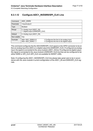
Examples
The following two samples show how the watchdog can be configured by means of the watch-
dog‘s I2
C interface and using the AT^SSPI command over RS-232/ASC0 to transfer the I2
C
user data. Please refer to [1] for more information on the AT command AT^SSPI and on how
to configure and control the data transfer over the Java module‘s I2
C interface.
The above Table 29 specifies the address register that can be used in I2
C configuration com-
mands.
The first example sets the level shifter‘s GPIO12 direction to “output“. It therefore configures a
write register marked as “W“ in Table 29. For more information on the configuration of GPIO
directions see Section 8.5.
Figure 24: Write data to address register
AT^SSPI=
CONNECT
<aD41401>
{a+}
<bD50001>
{b+00}
#
OK
Open the Java Terminals I2
C data connection.
Indicates that the connection is open.
WRITE command enclosed by <>: “a“ is a command ID to better identify and match
acknowledgments, “D4“ indicates the slave address (write mode), “14“ specifies
the address register GPIO12, and “01“ sets the data byte (i.e., line is “output“).
Note: The data byte value is only written if valid, i.e., if in the specified range. After
a WRITE command, the status code of the operation is saved to the status register
(SR) and a subsequent READ command from the status register will then return
the latest status code as listed in Table 30.
Acknowledgement enclosed in curly brackets of a successful data transmission.
READ command enclosed by <>: “b“ is a command ID to better identify and match
acknowledgements, “D5“ indicates the slave address (read mode), “00“ specifies
the address register SR, and “01“ sets the data length to be read. Note: The READ
command can only be called in conjunction with the SR address “00“ and the data
length of one byte “01“.
Acknowledgement enclosed in curly brackets of a successful data transmission,
together with the response code “00“ indicating that the command was successful-
ly executed.
Close data connection.
Connection closed.
External
Application
Watchdog
Write: Set GPIO12 to “output“
GPIO12:
01
SR:
00
Read from status register (SR)
Command
executed
successfully
E.g.,
RS-232
interface
Access to watchdog via Java Terminal interface and
Java module with its I2
C lines](https://image.slidesharecdn.com/m2mehs6thardware-190619161040/85/M2-m-ehs6t_hardware-81-320.jpg)
![Cinterion®
Java Terminals Hardware Interface Description
8.5 Configuring GPIO Directions
92
EHSxT_BGS5T_HID_v09 2017-04-25
Confidential / Released
Page 84 of 93
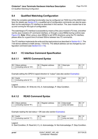
8.5.1 Configuration using I2
C Interface
Please refer to Section 8.4 for more information on how to configure the watchdog via I2
C in-
terface.
Figure 26 explains the configuration steps required to set the Java Terminals‘s GPIO7 signal
direction to OUTPUT (default direction is INPUT):
Figure 26: Setting GPIO direction to OUTPUT via I2
C interface
Figure 27 shows the configuration steps required to re-set the Java Terminals‘s GPIO7 signal
direction to INPUT:
Figure 27: Setting GPIO direction to INPUT via I2
C interface
For more information on the AT commands mentioned in the above figures see also [1].
Note: When using a Java MIDlet to set GPIO directions using the I2
C interface, please allow
for a guard time of at least 500ms between two I2
C commands.
GPIO connector Java module
Level shifterGPIO7 GPIO7
Set level shifter to OUTPUT using AT^SSPI and
a specific read/write protocol over I2
C interface *
Level shifterGPIO7 GPIO7
Set GPIO7 at Java module to OUTPUT with
GPIO command AT^SCPIN=1,6,1
Now, IO state can be set with AT^SSIO=6,0
Steps:Voltage level conversion
Java Terminal = INPUT = OUTPUT
* See Section 8.4.1.4 for configuration details.
* See Section 8.4.1.4 for configuration details.
GPIO connector Java module
Level shifterGPIO7 GPIO7
Level shifterGPIO7 GPIO7
Voltage level conversion
Java Terminal = INPUT = OUTPUT
Set GPIO7 at Java module to INPUT with
GPIO command AT^SCPIN=1,6,0
Set level shifter to INPUT using AT^SSPI and
a specific read/write protocol over I2
C interface *
Now, GPIO7 can be read out with AT^SGIO=6
Steps:](https://image.slidesharecdn.com/m2mehs6thardware-190619161040/85/M2-m-ehs6t_hardware-84-320.jpg)
![Cinterion®
Java Terminals Hardware Interface Description
8.5 Configuring GPIO Directions
92
EHSxT_BGS5T_HID_v09 2017-04-25
Confidential / Released
Page 85 of 93
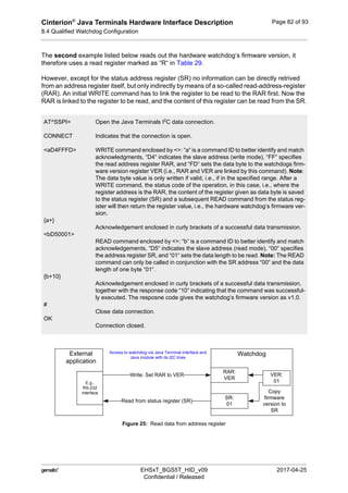
8.5.2 Configuration using TXD0 Line of ASC0 Interface
Please refer to Section 8.3 for more information on how to configure the watchdog via TXD0
line of ASC0 interface.
Figure 26 explains the configuration steps required to set the Java Terminals‘s GPIO7 signal
direction to OUTPUT (default direction is INPUT):
Figure 28: Setting GPIO direction to OUTPUT via TXD0 line (at 1200bps)
Figure 26 shows the configuration steps required to re-set the Java Terminals‘s GPIO7 signal
direction to INPUT:
Figure 29: Setting GPIO direction to INPUT via TXD0 line (at 1200bps)
For more information on the AT commands mentioned in the above figures see also [1].
GPIO connector Java module
Level shifterGPIO7 GPIO7
Set level shifter to OUTPUT with watchdog
command WD=GPIO_DIR,527,14 *
Level shifterGPIO7 GPIO7
Set GPIO7 at Java module to OUTPUT with
GPIO command AT^SCPIN=1,6,1
Now, IO state can be set with AT^SSIO=6,0
Steps:Voltage level conversion
Java Terminal = INPUT = OUTPUT
* See Section 8.3.1.11 for configuration details.
GPIO connector Java module
Level shifterGPIO7 GPIO7 Set level shifter to INPUT with watchdog
command WD=GPIO_DIR,525,12 *
Now, GPIO7 can be read out with AT^SGIO=6
Level shifterGPIO7 GPIO7
Set GPIO7 at Java module to INPUT with
GPIO command AT^SCPIN=1,6,0
Steps:Voltage level conversion
Java Terminal = INPUT = OUTPUT
* See Section 8.3.1.11 for configuration details.](https://image.slidesharecdn.com/m2mehs6thardware-190619161040/85/M2-m-ehs6t_hardware-85-320.jpg)