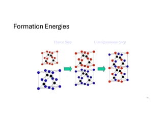
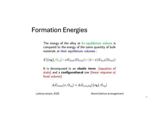
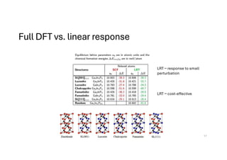
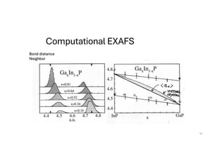
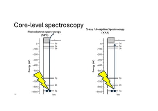
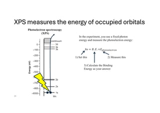
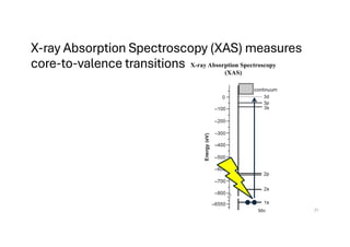
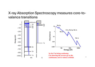
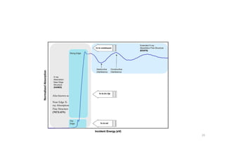
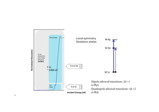
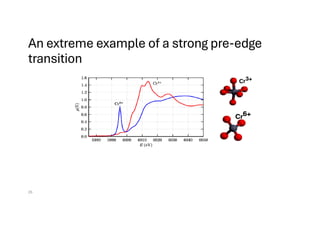
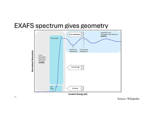
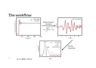
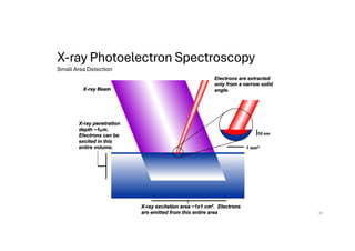
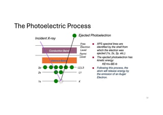
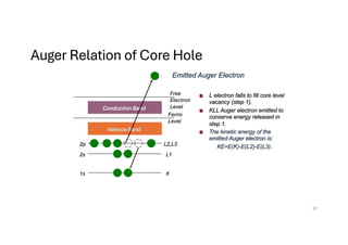
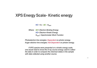
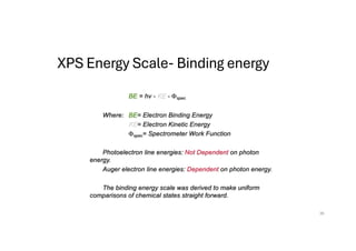
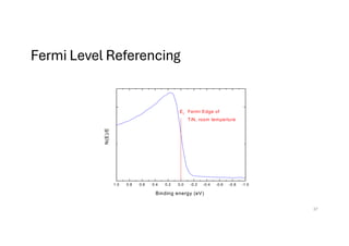
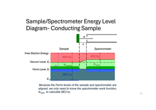
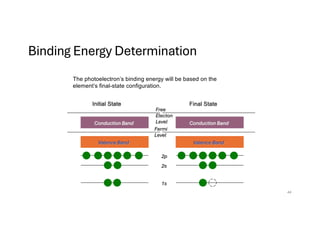
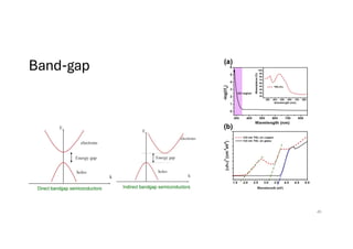
The document discusses non-Boltzmann sampling, experimental techniques such as X-ray photoelectron spectroscopy (XPS) and X-ray absorption spectroscopy (XAS), and their applications in analyzing semiconductor alloys and nanostructures. It covers the theoretical foundations of these methods, including the calculation of binding energies and the effects of disorder on material properties. The lecture emphasizes the importance of understanding electronic structures and thermodynamic properties in material science.

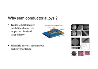
![Allow non-equal a-priori probabilities to get less possible moves that are not accepted
Wo
= f DH
ij [ ij ]
ji
Wo
ji
= f[DH ]
In Metropolis this is symmetric
Detailed balance
PWo
P = P W o
P
i ij ij j ji ji
Pij
ji
=
f DHij
[ ]
ji
P f[DH ] ij
exp(-bDH )
Non-Metropolis Monte Carlo
4](https://image.slidesharecdn.com/lecture-12-241119164047-5f478fb4/85/Lecture-12-atomistic-simulation-of-materials-4-320.jpg)
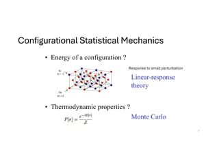

![Free electrons (those giving rise to conductivity) find
an equal potential which is constant throughout the material.
Fermi-Dirac Statistics:
f(E) = 1
exp[(E-Ef)/kT] + 1
1.0
f(E)
0
0.5
Ef
1. At T=0 K: f(E)=1 for E<Ef
f(E)=0 for E>Ef
2. At kT<<Ef (at room temperature kT=0.025 eV)
f(E)=0.5 for E=Ef
T=0 K
kT<<Ef
Fermi Level Referencing
36](https://image.slidesharecdn.com/lecture-12-241119164047-5f478fb4/85/Lecture-12-atomistic-simulation-of-materials-36-320.jpg)


![Polymer [ बहुलक ] Chemistry Notes PDF - Irfanullah Mehar - JJ Sir Chemistry.pdf](https://cdn.slidesharecdn.com/ss_thumbnails/polymerchemistrynotespdf-irfanullahmehar-jjsirchemistry-260210172118-3f9b37f7-thumbnail.jpg?width=640&height=640&fit=bounds)


